I. INTRODUCTION
Studying the deformation mechanisms in the nanoscale metallic multilayered composite materials has increasingly become both an interesting topic scientifically and an important subject technologically during these recent years, especially with the oncoming development of the new generations of nuclear energy systems. Nanoscale metallic multilayered composite materials are interesting due to their unusual mechanical properties such as very high flow strength and stable plastic flow to large strains.Reference Misra, Hirth and Hoagland1–Reference Demkowicz, Hoagland and Hirth3 The interface-dominated plasticity mechanisms have been theoretically proposed to be the origin of these unique mechanical properties in nanoscale composite materials.Reference Misra, Demkowicz, Wang and Hoagland4, Reference Hoagland, Hirth and Misra5 Studying especially experimentally how the dislocation configurations and densities evolve during deformation thus will be crucial in highlighting the yield, work hardening, and recovery mechanisms in the nanolayered materials.
However, previous studiesReference Anderson, Bingert, Misra and Hirth6, Reference Nyilas, Misra and Ungar7 on deformation of metallic multilayered composite materials have been largely done ex situ and using a conventional laboratory x-ray diffraction (XRD) technique that sampled a rather large area of the material (∼hundreds of microns). Lacking the sensitivities needed in the deformation of such small length scale materials, these studies did not reveal much contrast in terms of dislocation density and cell structure formation within layers between before and after the deformation.Reference Anderson, Bingert, Misra and Hirth6, Reference Nyilas, Misra and Ungar7 In situ study of metallic multilayered thin films utilizing a high brilliance synchrotron source and mesoscale (tens to hundreds of microns) x-ray beams was conducted by Aydiner et al.,Reference Aydiner, Brown, Mara, Almer and Misra8, Reference Aydiner, Brown, Misra, Mara, Wang, Wall and Almer9 resulting in the measurements of residual stress prior to deformation and elastic–plastic transition during tensile straining. However, as inherent in the tensile deformation mode of materials, samples would be more prone to fracture (as opposed to in compression deformation) before much plasticity could be studied. This is especially true for the multilayers with individual layer thickness smaller than 30 nm as was observed by Aydiner et al.Reference Aydiner, Brown, Mara, Almer and Misra8, Reference Aydiner, Brown, Misra, Mara, Wang, Wall and Almer9
Our most recent success in growing nanoscale single-crystal metallic multilayered composite materialsReference Budiman, Li, Baldwin, Xiong, Luo, Wei, Tamura, Kunz, Chen and Misra10 thus combined with the synchrotron-based Laue microdiffraction technique utilizing a focused x-ray beam into the submicron scale (i.e., hundreds of nanometers) of white beam (polychromatic) radiationReference Tamura, MacDowell, Spolenak, Valek, Bravman, Brown, Celestre, Padmore, Batterman and Patel11, Reference Swygenhoven, Schmitt, Derlet, Petegem, Cervellino, Budrovic, Brandstetter, Bollhalder and Schild12 and the recent advances in micropillar compression testing in a synchrotron beamline setupReference Budiman, Han, Greer, Tamura, Patel and Nix13, Reference Maass, Petegem, Swygenhoven, Derlet, Volkert and Grolimund14 would finally enable us to do experiments with significantly fewer shortcomings of the above previous studies.Reference Anderson, Bingert, Misra and Hirth6–Reference Aydiner, Brown, Misra, Mara, Wang, Wall and Almer9 The micropillar compression setup enables us to experiment with nanolayers of less than 30-nm individual layer thickness. The synchrotron x-ray microdiffraction (μXRD) technique provides a much smaller and thus higher sensitivity probe for the nanolayer deformation compared to the other x-ray techniques described in the above previous studies.Reference Anderson, Bingert, Misra and Hirth6–Reference Aydiner, Brown, Misra, Mara, Wang, Wall and Almer9 Because it is a Laue technique using the white beam nature of synchrotron radiation, this approach can further provide us with the quantitative examination of dislocation densitiesReference Valek15, Reference Budiman16 and configurationsReference Budiman16 and thus how they might evolve during the deformation in the nanoscale multilayered composite materials. Furthermore, this information will be obtained over a meaningful area of observation in the sample, in contrast to in situ straining in a transmission electron microscope (TEM) that is useful in studying the unit processes of dislocation nucleation, multiplication, and annihilation.Reference Budiman, Li, Baldwin, Xiong, Luo, Wei, Tamura, Kunz, Chen and Misra10
The synchrotron technique of scanning white beam μXRD has been described thoroughly elsewhere.Reference Tamura, MacDowell, Spolenak, Valek, Bravman, Brown, Celestre, Padmore, Batterman and Patel11, Reference Swygenhoven, Schmitt, Derlet, Petegem, Cervellino, Budrovic, Brandstetter, Bollhalder and Schild12, Reference Valek15, Reference Budiman16 The power of this technique as a local nanoplasticity probe stems from the continuous range of wavelengths in a white x-ray beam, allowing Bragg’s Law to be satisfied even when the lattice is locally rotated or bent, resulting in the observation of asymmetric broadening (streaking) in the Laue diffraction peaks. Since geometrically necessary dislocations (GNDs) are directly related to the local lattice curvature, the technique of scanning x-ray microdiffraction (μSXRD) using a focused polychromatic/white synchrotron x-ray beam can be used to determine the density of GNDs.Reference Valek15, Reference Budiman16 This has proven to be useful in the study of plasticity involving small-scale samples of various materials using both ex situReference Kirchlechner, Kiener, Motz, Labat, Vaxelaire, Perroud, Micha, Ulrich, Thomas, Dehm and Keckes17–Reference Burek, Jin, Leung, Jahed, Wu, Budiman, Tamura, Kunz and Tsui21 and in situReference Maass, Petegem, Swygenhoven, Derlet, Volkert and Grolimund14, Reference Maass, Van Petegem, Ma, Zimmermann, Grolimund, Roters, Van Swygenhoven and Raabe22, Reference Maass, Van Petegem, Grolimund, Van Swygenhoven, Kiener and Dehm23 approaches, as well as in the study of plasticity in technologically important small-scale structures in advanced microelectronics industry.Reference Budiman, Nix, Tamura, Valek, Gadre, Maiz, Spolenak and Patel24–Reference Budiman, Hau-Riege, Baek, Lor, Huang, Kim, Neubauer, Pak, Besser and Nix27
Using this approach, we studied the deformation mechanisms in the nanolayered materials using ex situ pillar compression setup (i.e., the same pillar, we characterized between before and after the deformation). We monitored the change in the Laue diffraction peaks before and after uniaxial compression of a nanoscale Cu/Nb single-crystal multilayer pillar. A quantitative analysis of the Laue peak widths then allowed us to estimate the density of statistically stored dislocations (SSDs) in the pillar. A comparison of the numbers of SSDs before and after the uniaxial compression furthermore provided indications about the change in microstructure associated with plastic deformation.
II. EXPERIMENTAL
The single-crystal Cu/Nb nanoscale multilayers were grown by electron beam evaporation on single-crystal a-cut sapphire  substrates (MTI Corporation, Richmond, CA) at elevated temperature of 200 °C. Deposition was performed under a vacuum environment of at least 5 × 10⁻⁸ Torr at rates of 0.5 nm/s for Nb and 5 nm/s for Cu. Total thickness was about 0.6 μm and individual layer thickness of both Cu and Nb was 20 nm. The multilayer structure was formed by alternatively depositing layers of Nb and Cu. The first layer deposited was Nb, and it was deposited at the elevated temperature of 950 °C for improved structural integrity with the substrate and the low deposition rate of 0.5 nm/s for improved orderly growth of the film as the seed layer for subsequent layers of both Cu and Nb. The subsequent Nb layers were deposited at the elevated temperature of 200 °C and low deposition rate of 0.5 nm/s while all Cu nanolayers were deposited at the elevated temperature of 200 °C and high deposition rate of 5 nm/s to achieve good quality and thermally stable (i.e., continuous layers) single-crystal multilayers. The growth of these nanoscale Cu/Nb single-crystal multilayers has been described thoroughly elsewhere.Reference Budiman, Li, Baldwin, Xiong, Luo, Wei, Tamura, Kunz, Chen and Misra10
The first Nb layer grew epitaxially and strongly {110} textured on the single-crystal sapphire  substrate with only three in-plane variants (all {110} textured but have different in-plane orientations, each shifted 60° from another). Subsequently, the Cu and Nb layers grew epitaxially and strongly {111} and {110} textured, respectively, on each other, and similarly with only two in-plane twin variants of Cu and the three in-plane variants mentioned above for Nb. The orientation relationship between the multilayered film and the substrate was found to be
 . This microstructure has been described completely and confirmed with both XRD method of phi-scans and the synchrotron x-ray Laue microdiffraction technique in our earlier work.Reference Budiman, Li, Baldwin, Xiong, Luo, Wei, Tamura, Kunz, Chen and Misra10
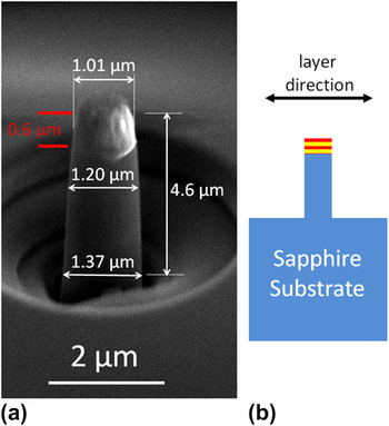
The pillars were fabricated utilizing the annular milling method of focused ion beam (FIB) machining,Reference Volkert and Lilleodden28 where a Ga+ ion beam is used to remove materials to shape a sample to high precision.Reference Uchic, Dimiduk, Florando and Nix29, Reference Tamura, Kunz, Chen, Celestre, MacDowell and Warwick30Figure 1(a) shows such a pillar with nominal dimensions of diameter of about 1.20 μm and height of about 4.6 μm of which only the top 0.6 μm is the Cu/Nb 20 nm/20 nm single-crystal multilayered film as shown with the red lines in Fig. 1(a) and also shown schematically (with red and yellow layers) in Fig. 1(b); the bottom 4 μm of the pillar is the single-crystal sapphire substrate. The layer direction is perpendicular to the cylinder axis. The pillars were such as at the time of the sample preparation for this study; we were not able yet to grow more than 0.6-μm-thick film of Cu 20 nm/Nb 20 nm single-crystal multilayers with thermally stable and continuous layers of both Cu and Nb.Reference Budiman, Li, Baldwin, Xiong, Luo, Wei, Tamura, Kunz, Chen and Misra10 This approach was thus chosen due to our limited access to better and more advanced FIB equipment at Los Alamos National Laboratory (LANL) that is more capable of routinely producing submicron diameter pillars that would have been needed if we were to satisfy the usual desired aspect ratio of 1:3 for pillar compression testing.
The micron-size Cu 20 nm/Nb 20 nm single-crystal multilayered materials pillar specimen; (a) the scanning electron microscope (SEM) image showing the 0.6-μm-thick Cu/Nb single-crystal multilayer film on the top of the pillar—the bottom 4 μm of the pillar is the single-crystal sapphire substrate—fabricated using focused ion beam (FIB) machining and shown with dimensions, and (b) the schematic illustration of the pillar specimen.

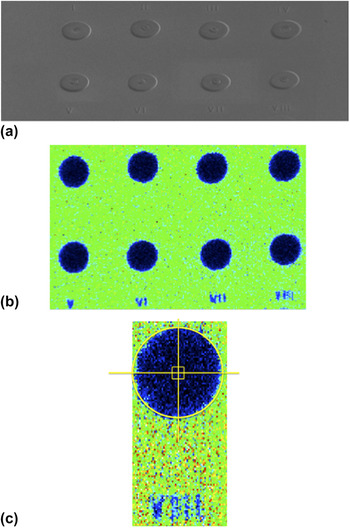
As the nanoscale Cu/Nb multilayered film that is the subject of the deformation study here is only the top 0.6 μm of the pillar, the diameter at the top of the pillar, which is 1.01 μm, is more meaningful to refer to when the results of the pillar compression tests are described. As evident from Fig. 1(a), a moderate taper is commonly found in the pillars in this study. Circular craters, 50 μm in diameter, were first carved out of the Cu/Nb single-crystal film, leaving behind only the micropillars at the centers of the craters as shown in the scanning electron microscope (SEM) image in Fig. 2(a). Figure 2(b) shows the corresponding synchrotron x-ray microfluorescence (μXRF) mapping of the Cu element. Once a particular crater for instance with a pillar of interest was found by μXRF mapping, the exact location of that particular pillar was specified such as illustrated in Fig. 2(c), and thus fine diffraction (synchrotron white beam Laue microdiffraction—μXRD) scanning could be done around the location of the pillar of interest. While the x-ray beam has a full-width at half-maximum (FWHM) of 0.8 μm × 0.8 μm, it does also have long tails as typically found in the x-ray microbeam focused by Kirkpatrick–Baez mirrors.Reference Tamura, Kunz, Chen, Celestre, MacDowell and Warwick30 This effectively reduces the resolution of the technique. However, in this particular study, given the large crater, we have high confidence that no spurious signal was picked up from the Cu/Nb materials outside the crater; thus, the signal that we obtained from the μXRD of the pillar would genuinely provide insights about deformation in the Cu and Nb nanolayers of the particular pillar. The fine μXRD scan area could be something like shown in Fig. 2(c) as a small square right at the center of the crater.
The pillar specimen preparation; (a) the array of eight pillars each exactly in the middle of a crater of 50-μm diameter fabricated using FIB machining and used to help locate the pillar: SEM image, and (b) the corresponding synchrotron white beam x-ray microfluorescence (μXRF) scan showing the number markers (V–VIII) as in the SEM image; (c) once a crater is identified (for example, in the present study, we presented data from Pillar VIII as shown in the enlarged individual XRF scan), the exact position of the pillar is known and based on that fine diffraction scan was performed to obtain Laue diffraction patterns from the Cu and Nb single-crystal nanolayers.

The uniaxial compression testing of these pillars was conducted using an Agilent/MTS Nanoindenter XP (Santa Clara, CA) with a flat punch diamond tip. The nanoindenter, which is a load-controlled instrument, was programmed to perform a nominally displacement-controlled test. In this method, the displacement rate is calculated continuously during the compression test based on the measured displacement and time. When the measured displacement rate is below a specified value, the load is adjusted to maintain that particular displacement rate. This method is designed to simulate a constant displacement rate. Load–displacement data were collected in the continuous stiffness measurement mode of the instrument. The data obtained during compression were then converted to uniaxial true stresses and strains using the assumption that the plastic volume is conserved throughout this mostly homogeneous deformation.
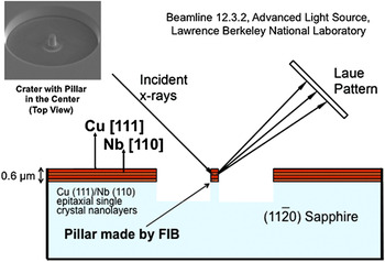
The white beam μXRD experiment (Fig. 3) was performed on beamline 12.3.2 at the Advanced Light Source, Berkeley, CA. The sample was mounted on a precision XY MICOS stage (Eschbach, Rhineland-Palatinate, Germany), and the pillar of interest was raster scanned at room temperature under the x-ray beam before and after the uniaxial pillar compression (ex situ); this provided μXRF and μXRD scans for the area near the pillar. The focused x-ray beam size was 0.8 μm × 0.8 μm (FWHM). The μXRD patterns were collected using a MAR133 x-ray charge-coupled device (CCD) detector and analyzed using the XMAS software package. We started with eight Cu/Nb pillars [as shown in Fig. 2(a)] but in the end we had complete data (initial synchrotron μXRD characterization, stress–strain curve, and final μXRD characterization) for only three pillars (data from other pillars were not included due to nonuniform pillar compression as well as nonsymmetrical pillar geometry due to variations in FIB machining). Results from the three pillars were found consistent with each other within the experimental variations expected from the utilized techniques. The case of one particular pillar is presented in full in this manuscript as a representative of the overall finding from the three pillars in the present study.
A schematic illustration of the synchrotron white beam x-ray microdiffraction (μXRD) experiments (conducted at the ALS beamline 12.3.2, Lawrence Berkeley National Lab) on the nanoscale Cu/Nb single-crystal multilayered materials pillar on sapphire substrate. (The SEM image of a crater with a pillar on the left upper corner is just provided as generic example, not as an image of the the actual pillar/crater studied in the present study).

III. RESULTS AND DISCUSSION
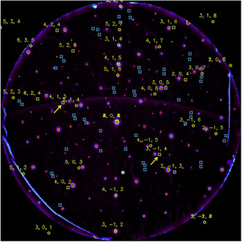
Figure 4 shows the Laue diffraction image taken at the location of the single-crystal Cu/Nb multilayer pillar (i.e., one of the three pillars with complete data; from now on in this manuscript, we will refer only to this particular pillar for all data and images; however, the discussion applies generally for all the three pillars) before uniaxial compression. The Laue diffraction image is basically very similar to the two-dimensional (2D) reciprocal space map of the sample except that it is not a map of the scattering vectors (q) but rather it is a map of the diffracted beam vectors (kout). It thus can be converted into the 2D reciprocal space map simply through the geometrical parameters of the experimental setup. Figure 4 shows where the diffracted x-ray beams hit the 2D CCD detector, and thus, from their relative positions in the CCD frame we can obtain the angles between the vectors and in turn the information about the crystallographic planes in the diffracted volume of the sample. The x- and y-coordinates in the CCD frame can thus be translated into angles of 2θ and χ angles, which hold their typical definitions in conventional laboratory XRD. After background subtraction and a peak search and fitting routine, the positions of all reflections in the CCD frame are established and thus the Laue pattern can be indexed with Miller indices.
The Laue diffraction pattern obtained from the micron-size Cu 20 nm/Nb 20 nm single-crystal multilayered materials pillar specimen under synchrotron μXRD showing one set of Nb indexation (the yellow indices—the diffraction peaks whose positions are as indicated by the yellow squares are not actually visible at this magnification due to low intensities) indicating single-crystal Nb nanolayers with the [202] out-of-plane orientation as indicated by the Laue diffraction peak at the center of the pattern; the two yellow arrows point to the particular Nb Laue diffraction peaks—the Nb  and
 —that will be discussed further in the manuscript as presented subsequently in Figures 5(a) and 7.

A set of indexation (with yellow Miller indices—the diffraction peaks whose positions are as indicated by the yellow squares are not actually visible at this magnification due to low intensities) is shown in Fig. 4 belonging to a Nb crystal with out-of-plane orientation of [110] as expected in our multilayer system. This indicates the film of the pillar consists entirely of one in-plane variant of the [110] Nb, even though our previous film characterizationReference Budiman, Li, Baldwin, Xiong, Luo, Wei, Tamura, Kunz, Chen and Misra10 suggests there are three in-plane variants of Nb. However, as shown in Ref. Reference Budiman, Li, Baldwin, Xiong, Luo, Wei, Tamura, Kunz, Chen and Misra10, there is a peak pair (separated by 180°) in the phi-scan of Nb that is much higher in intensities than the other two pairs. This strongly suggests that one of the variants of Nb covered a larger area in the film, and it thus appears very likely that our pillar was machined where this dominant in-plane variant of Nb lies in the film. To verify this hypothesis, we went to different locations in the film and took the μXRD reflections of the Cu and Nb layers in various spots of the film separated by hundreds of microns to even millimeters. The results confirmed our hypothesis, and within the same film we managed to get two other distinct indexations of [110] Nb in addition to the one presented in Fig. 4.
The two yellow arrows in Fig. 4 pointed to two representative Nb Laue diffraction peaks that will be discussed in greater details in the following paragraphs. The Nb Laue diffraction peaks were not visible at this magnification as they are rather diffuse (compare those with the very bright—i.e., with red color, which means high intensity; the bigger the red areas the higher the intensities—and very symmetrical diffraction peaks that are not indexed in Fig. 4; they belong to the sapphire substrate). However, when we go to higher magnification as will be shown later in Fig. 5, these peaks of the Nb nanolayers will be visible as well as easily recognizable by the peak search routine of our custom-made μXRD data analysis software program—XMAS.Reference Tamura, MacDowell, Spolenak, Valek, Bravman, Brown, Celestre, Padmore, Batterman and Patel11, Reference Valek15 The broad diffraction peak is consistent with the rather small size of the individual Nb crystals (the individual layer thickness of each layer of Nb is only 20 nm).
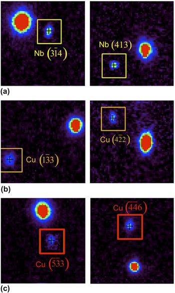
The enlarged images of the representative Nb and Cu Laue diffraction peaks from before the deformation showing rather diffuse peaks especially as they are being contrasted (in the same images) with the nearest sapphire substrate peaks (the big red-colored diffraction peaks); (a) the Nb  and
 in yellow-colored boxes, (b) the Cu
 and
 in orange-colored boxes indicating the first Cu crystal, and finally (c) the Cu
 and
 in red-colored boxes indicating the second Cu crystal. All images have the same magnification and intensity threshold level and thus can be compared directly.

The very bright and symmetrical peaks in Fig. 4 belonging to the sapphire substrate as mentioned above were not shown with the sapphire indexation. Although not shown, the indexation of sapphire indeed confirms that its out-of-plane orientation is  . The remaining captured diffractions peaks were shown in blue squares in Fig. 4 and were not shown with the Miller indices. They represent the Cu crystals, and their indexations confirm the existence of two Cu crystals both with the same [111] out-of-plane orientations with 60° in-plane rotation about their [111] axis of each other as has been reported in our previous studyReference Budiman, Li, Baldwin, Xiong, Luo, Wei, Tamura, Kunz, Chen and Misra10 with the complete Cu indexations.
Figure 5(a) shows the enlarged images of two representative Nb diffraction peaks, marked with yellow arrows in Fig. 4, while Figs. 5(b) and 5(c) show the enlarged images of the two corresponding peaks, which are representative of each of the two Cu crystals in the nanolayers. They thus represent the initial states of the Nb and Cu crystals in the pillar (i.e., before deformation). They show rather diffuse peaks (i.e., with green and blue colors which mean lower intensities) especially as they are being contrasted (in the same captured image) with the nearest sapphire peaks (the big red-colored diffraction peaks). This was done to observe shifts in the positions of the Nb and Cu Laue peaks associated with the deformation in the film of the pillar. Since the sapphire substrate should not be deformed to any significant extent (both elastically or plastically) by the pillar compression of the Cu/Nb film, its Laue diffraction peaks could be considered stationary, and thus if the Nb or Cu Laue peaks change positions with respect to their nearest sapphire peaks upon the deformation, it would mean that there is crystal rotation or elastic deformation in the Nb and Cu crystals due to the deformation. Of course, we would know this too when we perform our indexation of the Nb and Cu crystals and obtained the complete strain tensor (minus the hydrostatic component) of the crystals and compare them between before and after the deformation. However, this way would provide us with the visualization of that information as later shown in Figs. 7–9.
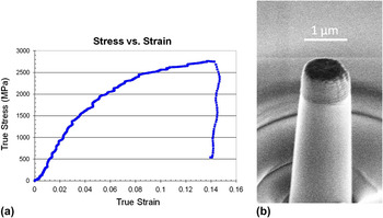
Figure 6(a) shows the stress–strain curves of the 1.01-μm-diameter pillar obtained during the compression testing. Uniaxial loading in the <111> direction of the Cu crystals in the film as well as in the <110> direction of the Nb crystal/layer, corresponding to the high-symmetry orientation, would result in the activation of multiple slip systems, with the film in the pillar deforming uniformly around its diameter as it is compressed as shown in Fig. 6(b). The flow stress reaches value as high as 2.7 GPa before the load was released at a plastic strain of about 14%. To ensure repeatability, three separate compression tests on other pillars were conducted and they have shown similar results to those in Fig. 6. The final diameter of the Cu/Nb film of the pillar after the uniaxial compression is 1.10 μm representing a 9% lateral strain, which is reasonably consistent with the total strain of 14% as indicated by the stress–strain curve in Fig. 6(a).
The uniaxial compression of the micron-size Cu 20 nm/Nb 20 nm single-crystal multilayered materials pillar specimen showing (a) the true stress—true strain curve indicating flow stresses reaching values as high as 2.7 GPa and a plastic strain of about 14%, as well as (b) SEM image of the uniaxially compressed pillar after the deformation indicating uniform deformation and the pillar preserving its cylindrical shape upon deformation.

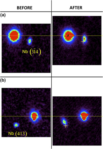
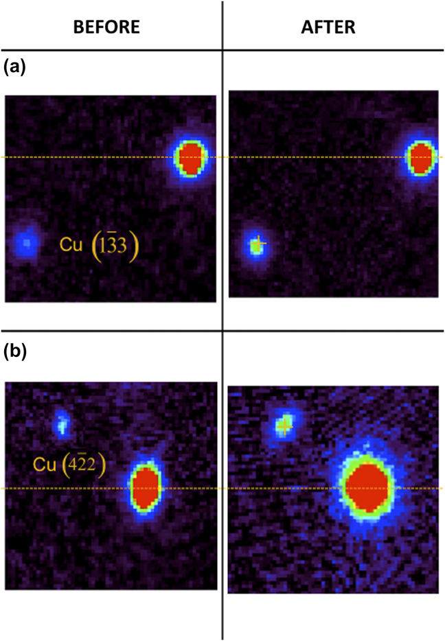
Figures 7(a) and 7(b) show the change in the shape and position of the Laue peaks of Nb  and
 crystal planes, respectively. The big and red-colored peaks here belong to the sapphire substrate, and they are used as references. Their shapes are nominally rounded as expected from a large perfect single crystal. If there is some irregularity, such as the horizontal streak in sapphire peaks as shown in Fig. 7 (after), then it is due to the saturation of the diffracted beam (a limitation of the CCD detector). The yellow-dotted horizontal lines in both Figs. 7(a) and 7(b) indicate the normalization of the sapphire peak position in the 2θ direction. The yellow plus signs indicate the initial positions of the Nb Laue peaks (i.e., before deformation) with respect to the position of the nearest sapphire peaks. Evidently, we observed that both Nb Laue peaks change in positions after the deformation as shown in Figs. 7(a) and 7(b). This change in the positions is significant as it involved more than a few pixels in the CCD detector as can be observed closely in Figs. 7(a) and 7(b). Later in the manuscript, this shift in the positions of Laue peaks will be confirmed with quantitative measurement [Fig. 10(c)] and also revisited in term of the elastic deviatoric (without the hydrostatic component) strain involved (Table I).
The side-by-side comparison of the same Laue diffraction peaks between before and after the uniaxial pillar compression showing (a) the Nb  and (b) the
 Laue diffraction peaks. The big red-colored peaks are again of the sapphire substrate and used as references (their positions in the 2θ axis are normalized with the yellow dotted line). The yellow plus signs indicate the positions of the Nb diffraction peaks (relative to those of the sapphire substrate) at the before deformation state (a departure from that position in the after deformation state as shown in this figure indicates elastic deviatoric deformation in the crystals/nanolayers during the uniaxial pillar compression).

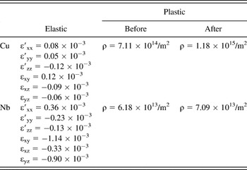
Quantitative summary of the both elastic (deviatoric) and plastic deformation in both Cu and Nb nanolayers involved in the uniaxial compression of Cu/Nb 20 nm/20 nm multilayered single-crystal pillar to about 14% strain.

Elastic (hydrostatic) strain was not measured in the present study. Dislocation density numbers here could be considered lower bound estimates. As has earlier been discussed in this manuscript, if arrays of interface dislocations from either side of the Cu/Nb interface effectively annihilate each other, such dislocation activities could not possibly be detected in the Laue diffraction peak broadening in the present study. Only the net plastic deformation here would be detected and thus the estimated dislocation density numbers would be lower bound.
The shapes of the Laue peaks provide us with the information about plastic deformation. Unlike in sapphire substrate, the Laue peaks from the Nb as well as the Cu nanolayers are far below the saturation level of the CCD detector (due to their small crystal sizes). Thus, any change in the shapes of the Laue peaks of Nb or Cu indicates real plastic deformation in the crystal that may be involved during the deformation. Figures 7(a) and 7(b), however, do not show significant change in the shapes as well as in the widths/sizes of the Nb Laue peaks. The Nb Laue peaks were already not so regular (i.e., rounded) in shapes even in the initial state (before deformation), and they remain largely the same shapes and sizes in the final state (after deformation). The initially not-so-rounded shapes of Nb Laue peaks suggest that there was plastic deformation already in the fabrication of the nanolayers (as Cu and Nb nanolayers accommodate misfits between each other during the deposition of the layers).
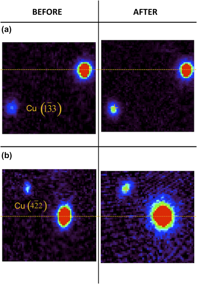
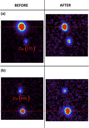
Figures 8(a) and 8(b) show the change in the shape and position of the Laue peaks of Cu  and
 crystal planes, respectively, from the first Cu crystal, while Figs. 9(a) and 9(b) show those of Cu
 and
 crystal planes, respectively, from the second Cu crystal in the nanolayer film of the pillar. The dotted horizontal lines and plus signs indicate the same features as described for Fig. 7. Evidently, here in Figs. 8 and 9, we observed no significant shift (not more than 1–2 pixel difference) in the position of the Cu Laue peaks after the deformation. This indicates there is not much elastic deviatoric strain involved in the deformation of the Cu nanolayers. This absence of significant shift will be confirmed also later in the manuscript with the actual quantitative measurement [Fig. 11(c)] and elastic deviatoric strain calculation (Table I).
The side-by-side comparison of the same Laue diffraction peaks between before and after the uniaxial pillar compression showing (a) the Cu  and (b) the
 Laue diffraction peaks. The dotted horizontal lines and plus signs indicate the same features as described for Figure 7.
The side-by-side comparison of the same Laue diffraction peaks between before and after the uniaxial pillar compression showing (a) the Cu  and (b) the
 Laue diffraction peaks. The dotted horizontal lines and plus signs indicate the same features as described for Figure 7.

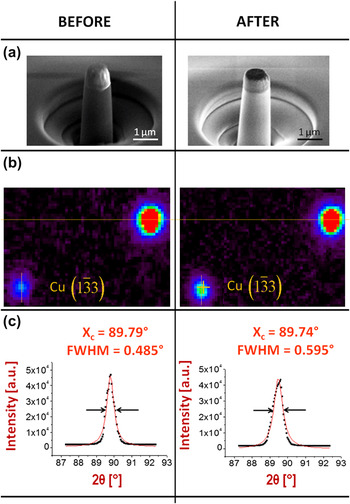
Although the Cu Laue peaks remain in approximately the same shapes after the deformation as evident from Figs. 8 and 9 (after), their sizes appear to be significantly larger compared to those from Figs. 8 and 9 (before). We confirmed this by quantitatively studying the intensity profiles of the Laue peaks and comparing the FWHM of the Cu Laue peaks between before and after the deformation. We selected the Nb  peak of Fig. 7(b) and the Cu
 peak of Fig. 8(a) from one of the Cu crystals to further present the quantitative data analysis of the intensity profile of the Laue diffraction peaks. These quantitative data analyses were shown in Figs. 10 and 11 (together with the SEM images of the nanopillar and the Laue peaks of the respective crystals that have been shown earlier) as a complete summary of what happened in Nb and Cu nanolayers, respectively. Care was taken to provide the intensity profile with respect to the 2θ angle at the χ angle in which the intensity is maximum to facilitate normalized comparison with other intensity profiles.
Further quantitative data analysis of a selected Laue diffraction peak from the micron-size Cu 20 nm/Nb 20 nm single-crystal multilayered materials pillar specimen as shown in (a) between before and after the uniaxial compression. The enlarged images of the selected Nb  diffraction peak between before and after the deformation were shown in (b) and their respective intensity profile in 2θ axis following the yellow solid lines indicated in (b) at a certain χ value, and their subsequent quantitative data analyses were shown in (c). The X c and FWHM are the location of the maximum intensity (in 2θ axis) and the full-width at half-maximum intensity (in 2θ angle), respectively, as measured based on the peak fitting.

Further quantitative data analysis of a selected Laue diffraction peak from the micron-size Cu 20 nm/Nb 20 nm single-crystal multilayered materials pillar specimen as shown in (a) between before and after the uniaxial compression. The enlarged images of the selected Cu  diffraction peak between before and after the deformation were shown in (b) and their respective intensity profile in 2θ axis following the orange solid lines indicated in (b) at a certain χ value, and their subsequent quantitative data analyses were shown in (c). The X c and FWHM hold the same definition as stated in Figure 10.
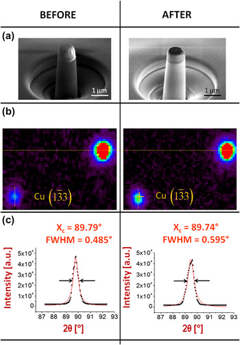
Figure 10(b) qualitatively shows that both Nb  Laue peaks have slightly different shapes (one is closer to being round shape while the other is a little streaked); however, upon closer and more quantitative examination, the difference actually involves not more than 2 pixels, and thus the difference could be considered minimal. Furthermore in Fig. 10(c), we take the intensity traces along a particular χ to study the Laue diffraction peak profile more quantitatively (here the χ angle is simply the angle orthogonal to the 2θ angle). The profiles were fitted with Lorentzian curves. The measured FWHMs of both profiles show that there is an increase of 0.034° in the angular width. However, this difference is barely over the experimental error bar of the instrument.Reference MacDowell, Celestre, Tamura, Spolenak, Valek, Brown, Bravman, Padmore, Batterman and Patel31 The angular resolution of this technique was calculated using a few assumptions on the experimental sample setup with respect to the CCD camera and on the capability of the indexing code,Reference Tamura, MacDowell, Spolenak, Valek, Bravman, Brown, Celestre, Padmore, Batterman and Patel11, Reference MacDowell, Celestre, Tamura, Spolenak, Valek, Brown, Bravman, Padmore, Batterman and Patel31 which are applicable to our micropillar compression experiments. The angular resolution in our experiments is signified by one CCD pixel difference, which translates to about 0.03° in the Laue peak measurement.Reference Tamura, MacDowell, Spolenak, Valek, Bravman, Brown, Celestre, Padmore, Batterman and Patel11, Reference MacDowell, Celestre, Tamura, Spolenak, Valek, Brown, Bravman, Padmore, Batterman and Patel31 Therefore, we can conclude based on our quantitative data analysis that the Nb Laue peaks are not significantly changed in shape nor are they significantly broadened.
Figure 10(c) also confirmed quantitatively what we have estimated earlier that there is a significant shift in the positions of the Laue peaks between before and after the deformation, which thus indicates elastic (deviatoric) strain. The center positions of the Laue peaks in 2θ—the X C—hown in Fig. 10(c) differ by 0.16° which is about 5–6 pixel difference consistent with what we can observe in Fig. 7(b). Complete indexation of the same Nb crystal of the film of the pillar between before and after the deformation provided us with the full transformation matrix associated with the deformation in the Nb nanolayers. This transformation matrix can be resolved into the rotational as well as the elastic deviatoric matrices, and we found that the rotational matrix indicates close to zero rotation and thus mostly just the elastic deviatoric deformation in Nb nanolayers. The complete elastic deviatoric strain tensor for Nb due to the pillar compression is shown in Table I.
Figure 11(b) shows qualitatively that both Cu  Laue peaks have rather similar shapes, i.e., largely rounded. The measured FWHMs of both profiles in Fig. 11(c) show that there is indeed an increase of 0.11° in the angular width. This broadening of the Cu Laue peak after the pillar compression is significant considering that the angular resolution of this technique in our experiments is 0.03° (as determined for the current experimental setup based on information presented in Refs. Reference Tamura, MacDowell, Spolenak, Valek, Bravman, Brown, Celestre, Padmore, Batterman and Patel11 and Reference MacDowell, Celestre, Tamura, Spolenak, Valek, Brown, Bravman, Padmore, Batterman and Patel31), which means the Laue peak here broadens by approximately 3–4 pixels. This extent of broadening cannot be neglected. Such peak broadening while maintaining the general rounded shapes of the Laue peaks after significant pillar deformation strongly suggests plastic deformation through accumulation of randomly distributed SSDs.
During the pillar compression, the deformation mechanism in the 20 nm/20 nm Cu/Nb multilayer film has been predicted to be the confined layer slip (CLS) that involves propagation of single dislocations to the interfaces in both layers.Reference Misra, Hirth and Hoagland1, Reference Misra, Demkowicz, Wang and Hoagland4, Reference Anderson, Foecke and Hazzledine32, Reference Phillips, Clemens and Nix33 Dislocations are confined to individual layers since the interface barrier stress to slip transmission is higher than the CLS stress. A schematic of symmetric slip activities on different slip systems during CLS in nanolayered materials is shown in Fig. 12(a) with one slip system in Cu nanolayer, for example, ended up depositing (as indicated by arrows) same-sign edge dislocations on the interface with Nb nanolayer in one direction, while other slip systems (not shown) on the same Cu nanolayer would deposit same-sign edge dislocations in other directions. Given the [111] out-of-plane orientation of the Cu crystals in the nanolayers, slip activity gets distributed on the mutliple available slip systems thereby promoting symmetry of slip activities within a given Cu nanolayer. As a consequence, the Cu Laue peaks broadened uniformly as we have observed in Figs. 8, 9, and 11 as randomly distributed SSDs ended up being accumulated in the interfaces with Nb nanolayers.
Schematic illustration of slip activities on different slip systems during confined layer slip in nanolayered materials (a) leading to concentration of like-signed edge dislocations in individual nanolayers which lead to local lattice curvatures of a certain magnitude |K| in many directions (b) resulting in the composite overall broadening of the Laue peak observed in the present study (c). There could be many more net geometrically necessary dislocations than as illustrated in this figure. Net GND #1–3 were just shown for simplicity and clarity. No dislocation activity was illustrated here in the Nb nanolayers indicating purely elastic deformation based on the findings of the present study, however there remains the possibility of annihilation of interface dislocations (i.e., plasticity followed by crystal recovery).

These dislocation arrays activated in the multiple slip systems available in the multiple Cu nanolayers of the composite material as illustrated schematically in Fig. 12(b) provide us with a methodology to estimate the SSD dislocation density increase that must be involved in the Cu nanolayers during the pillar deformation. When a single dislocation array in a certain direction was activated in the Cu nanolayers, it essentially introduced a net GND in the Cu crystals of the pillar, which would lead to asymmetric broadening of the Cu Laue peaks (streaking) in a certain direction. However, when multiple dislocation arrays were activated in multiple directions simultaneously in the Cu nanolayers with each of them causing the Cu Laue peaks to streak in each different direction, the end result of the observed Cu Laue peaks would be a composite of all those Laue peak streaking to many directions, which in the end would result as uniform Laue peak broadening as illustrated schematically in Fig. 12(c). This simple model provides us with a crude, first approximation method to estimate SSD density in the events of accumulation of dislocation arrays in multiple directions due to the deformation in the nanolayers.
Such plastic deformation was not significantly observed in the Nb nanolayers as evident from our observations in Figs. 7 and 10. The Nb Laue peaks were not significantly broadened or significantly changed in shapes indicating no evidence of significant plasticity was involved in the deformation. The deformation in Nb nanolayer appears thus to be mostly elastic as has also been suggested by the elastic deviation strain tensor in Table I. However, this absence of a significant Laue peak broadening may not necessarily mean an absence of plastic deformation altogether in Nb nanolayers. It could also be because of arrays of interface dislocations from either side of the interface may effectively annihilate. Such events have been suggested in previous literature.Reference Misra, Hirth, Hoagland, Embury and Kung34 When the net of all slip activities in the Nb side of the interfaces is close to zero, then the Nb Laue peaks would be barely broadened. In this case therefore the absence of the Nb Laue peak broadening in our experiments is in effect a sign of a crystal recovery, while the Cu Laue peak broadening observed in this study thus indicates the net plastic deformation that is accommodated by the Cu nanolayers. Evidence of such annihilation of interface dislocations, however, could not possibly be obtained from an ex situ experiment such as done in the present study.
At 14% strain, the plasticity in Cu nanolayers while Nb nanolayers still deform mostly elastically could be an indirect evidence of the CLS mechanism that has been proposed earlier.Reference Misra, Hirth and Hoagland1, Reference Misra, Demkowicz, Wang and Hoagland4, Reference Anderson, Foecke and Hazzledine32, Reference Phillips, Clemens and Nix33 This is reasonable that the Cu nanolayers as the softer and more compliant phase in the composite would deform plastically first, while the harder and less compliant phase (i.e., Nb) is still more or less in elastic deformation. That is how we would expect the initial plastic flow would be accommodated in a deformation of such composite. Further straining, we believe then, would certainly introduce plastic deformation also in Nb nanolayers, which would subsequently cause the Nb Laue peaks in an experiment such as our present study to broaden significantly.
Figures 12(b) and 12(c) allow us to estimate the SSD dislocation density that must be involved in each of the Cu and Nb nanolayers during the pillar deformation. As the Laue peaks remain largely uniform in shapes after the deformation, the increase of the dislocation density in a given direction can be taken as a representative of the overall dislocation density increase in the crystal. The dislocation density, ρ, in a given direction can be calculated using the Cahn–Nye equation,Reference Cahn35–Reference Nye36ρ=|κ|/b, where |κ| is the local lattice curvature and b is the magnitude of the Burgers vector following the methodology described in our previous reports.Reference Valek15, Reference Budiman16, Reference Lee, Kim, Budiman, Tamura, Kunz, Chen, Burek, Greer and Tsui19, Reference Burek, Budiman, Jahed, Tamura, Kunz, Jin, Han, Lee, Zamecnik and Tsui20, Reference Budiman, Nix, Tamura, Valek, Gadre, Maiz, Spolenak and Patel24–Reference Budiman and Kim26 In our case here, the |κ|can be taken as the FWHM of the Laue peaks; thus, its increase would mean an increase in the dislocation density.
It is important, however, to recognize that this model represents a methodology to obtain estimate of dislocation density rather than its exact value. In addition, a few assumptions have to follow. First, parameters that can lead to Laue peak broadening, such as, instrumentation, crystal size, and initial dislocation density due to the fabrication process, must remain identical for all samples. It is clear in this study that all of these parameters are essentially the same for the pre- and postcompression XRD scans. Therefore, the only factor that affects the Laue peak broadening is solely originated from dislocation activities in the nanolayers during the pillar compression deformation.
Second, considering the above other sources of broadening are rather ambiguous and thus their precise identification is mostly unavailable but that they are nominally the same for both states of the Cu/Nb pillar (before and after pillar compression), it is more meaningful here to just compare the relative values between them (i.e., the difference in the FWHMs between before and after the deformation) and simply assume all other broadening contribution to be at a certain fixed level (independent of the pillar deformation) which for convenience and simplicity here could just be taken as zero. By doing so, we can just apply the Cahn–Nye equation directly to the observed FWHMs of the Laue peaks between before and after the deformation.
The SSD densities predicted using this approximation methodology based on the obtained values of FWHMs of the representative Cu and Nb Laue peaks (as shown in Figs. 10 and 11) between before and after the deformation are all revealed in Table I. Based on the SSD numbers there, we can conclude that there is a considerable increase in the dislocation storage in the Cu nanolayers after the deformation. Although the actual dislocation density increase may be rather small here, it is important to note that the SSD densities estimated using the above methodology could be considered lower bound numbers. As has earlier been discussed in this manuscript, if arrays of interface dislocations from either side of the Cu/Nb interface effectively annihilate each other, such dislocation activities could not possibly be detected in the Laue diffraction peak broadening in the present study. Only the net plastic deformation here would be detected and thus the estimated dislocation density numbers would be lower bound.
This finding together with an earlier finding using TEM reported by Misra et al.Reference Misra, Hirth, Hoagland, Embury and Kung34 on similar nanoscale Cu/Nb multilayers after heavy rolling to 60% reduction which did not reveal dislocation cell structure within the nanolayers thus suggest that the storage of dislocations may be located on the interfaces with Nb nanolayers. This is consistent with the proposed CLS mechanism.Reference Misra, Hirth and Hoagland1, Reference Misra, Demkowicz, Wang and Hoagland4, Reference Anderson, Foecke and Hazzledine32, Reference Phillips, Clemens and Nix33 However, this could not possibly be confirmed with the present x-ray observations alone. From the present experimental finding, thus, only the conclusion that there is considerable dislocation storage in the Cu nanolayers can be drawn.
This SSD increase detected by our μXRD technique has actually a rather significant meaning as a previous studyReference Nyilas, Misra and Ungar7 using laboratory XRD technique could not resolve significant difference in dislocation density between before and after rolling of similar Cu/Nb nanolayers to up to 150% elongation. Thus, this observation of Laue peak broadening in Cu nanolayers confirms the dislocation storage process such has been proposed earlier by Misra et al.Reference Misra, Hirth, Hoagland, Embury and Kung34
Table I also displays the complete elastic (deviatoric) strain tensor that was involved during the deformation in Cu nanolayers. The resolution of the strain measurement of this technique in our experiment is 10−4 based on the information presented in Refs. Reference Tamura, MacDowell, Spolenak, Valek, Bravman, Brown, Celestre, Padmore, Batterman and Patel11 and Reference MacDowell, Celestre, Tamura, Spolenak, Valek, Brown, Bravman, Padmore, Batterman and Patel31. The strain tensor numbers there suggest that while the Nb layers exhibit a fair amount of elastic (deviatoric) deformation, the Cu nanolayers exhibit insignificant amount of it (within the accuracy limit of the technique). This is again reasonable as the elastic deformation in the Cu nanolayers would have been relieved during pillar decompression/unloading. The elastic deformation in Nb nanolayers however would not be relieved (and thus would still be observed as indeed shown in Table I) as it is still held by the plastically deformed Cu nanolayers. However, the dilatational component of the elastic strain tensor (which is arguably the bulk of the elastic strain) were not actually obtained in the present study as white beam diffraction only allows measurement of the deviatoric components of the strain tensor. The calculation of the dilatational component of the strain tensor requires the monochromatic beam (single wavelength) measurement, which is beyond the scope of the present study. However, this information (the absolute elastic strain numbers) during the deformation of Cu/Nb multilayered materials has been obtained by Aydiner et al.Reference Aydiner, Brown, Mara, Almer and Misra8, Reference Aydiner, Brown, Misra, Mara, Wang, Wall and Almer9 That study, however, tested thicker individual layer thickness and textured (i.e., polycrystalline) Cu/Nb nanolayers as well as different mode and axis of deformation (tensile along the interface direction).
IV. CONCLUSIONS
Using synchrotron white beam x-ray submicron diffraction, we have studied deformation in Cu/Nb nanoscale single-crystal multilayer pillars, before and after uniaxial compression, and found evidence of SSD density increase in the Cu nanolayers caused by the plastic deformation. Our observation using synchrotron Laue μXRD thus confirms the dislocation storage process that has been proposed earlier in the literature for nanolayers which has not hitherto been detected with other characterization techniques. The absence of significant storage of dislocation in the Nb nanolayers in this study meanwhile could be a sign of crystal recovery that has also been proposed for nanolayers.
ACKNOWLEDGMENTS
The authors gratefully acknowledge critical support and infrastructure provided for this work by the Department of Energy (DOE), Office of Science, Office of Basic Energy Sciences. We thank R.G. Hoagland and J.P. Hirth for insightful discussions. W.D. Nix is gratefully acknowledged for his support in providing the nanomechanical testing facility at Stanford. The Advanced Light Source is supported by the Director, Office of Science, Office of Basic Energy Sciences, Materials Sciences Division of the U.S. Department of Energy under Contract No. DE-AC02-05CH11231 at Lawrence Berkeley National Laboratory and University of California, Berkeley, California. The move of the microdiffraction program from ALS beamline 7.3.3 onto to the ALS superbend source 12.3.2 was enabled through the NSF Grant No. 0416243. One of the authors (ASB) is supported by the Director, Los Alamos National Laboratory (LANL), under the Director’s Postdoctoral Research Fellowship program (LDRD/X93V). The research at KAIST was supported by National Research Foundation of Korea under Contract N01110283 and the KINC grant at KAIST under Contract N10110033.