I. INTRODUCTION
FSSs are flat composite metal screens designed to be transparent for some frequency bands while reflecting or absorbing other frequency bands [Reference Munk1]. Frequency-selective surfaces (FSSs) are used in many applications which include RCS reduction, Electromagnetic shielding, dichroic reflectors, etc. [Reference Parker2, Reference Chiu, Kuo and Lin3]. Prodigious growth in ultra-wideband (UWB) systems due to its high data rate and short pulse transmission demands UWB FSS for broad band shielding [Reference Syed, Ranga, Matekovits, Esselle and Hay4]. Many techniques are followed to increase the bandwidth of FSS [Reference Syed, Ranga, Matekovits, Esselle and Hay4–Reference Baisakhiya, Sivasamy, Kanagasabai and Periaswamy11]. FSS made of cross-dipoles and rings on both sides of a single-layer FR-4 substrate used to obtain wideband shielding is discussed in [Reference Syed, Ranga, Matekovits, Esselle and Hay4]. It provides a bandwidth of 7.5 GHz ranging from 6.5 to 14 GHz with the unit-cell dimension of 0.26 × 0.26 λ o, which may be further increased to operate in the lower frequency range at the cost of operational bandwidth. FSSs exhibiting UWB response realized using multilayer FSS is illustrated in [Reference Huang, Zhang and Hu6, Reference Ranga, Matekovits, Esselle and Weily7]. In [Reference Huang, Zhang and Hu6], the front to back ratio characteristics of UWB antenna is enhanced by employing an UWB FSS as the reflector element. The FSS is a four-layered structure with the dimension of 15 × 15 mm which provides a wider bandwidth ranging from 2.7 to 13.2 GHz. In the notion of antenna gain improvement, dual-layer FSS with the unit-cell dimension of 17 × 17 mm is used in [Reference Ranga, Matekovits, Esselle and Weily7].
The FSS provides a wide stop band performance from 4 to 12 GHz. Multilayer FSS delivers UWB response but limits their use in applications demanding simple FSS geometry. In [Reference Li, Yang, Zhang and Wu8, Reference Kushwaha, Kumar, Ram Krishna and Oli9], polarization-selective single-layer FSS exhibiting UWB characteristics are illustrated. Polarization-selective response is attributed to the asymmetric nature of the FSS unit cells. Polarization independency is also an important factor for better frequency-selectivity performance which is obtained by using symmetric FSS structures in [Reference Li, Zhang, Yang, Wu and Hua10, Reference Baisakhiya, Sivasamy, Kanagasabai and Periaswamy11]. A novel FSS prototype exhibiting UWB characteristics discussed in [Reference Li, Zhang, Yang, Wu and Hua10] provides a bandwidth of 51.24% (4.2–6.98 GHz) where stop band characteristics in the lower range of frequencies are achieved by varying the dimension of the FSS from 0.12λ o × 0.12λ o to 0.17λ o × 0.17λ o. Therefore, the bandwidth characteristics deteriorate from 51.24 to 49.19%. In [Reference Baisakhiya, Sivasamy, Kanagasabai and Periaswamy11], a compact UWB FSS of size 8 × 8 mm2 operating in a wideband ranging from 7.04 to 10.55 GHz at −20 dB reference level of insertion loss is reported. Single-layer FSS illustrated in [Reference Li, Zhang, Yang, Wu and Hua10, Reference Baisakhiya, Sivasamy, Kanagasabai and Periaswamy11] is of less bulky but provides narrow bandwidth compared with multilayer FSS. From the literature it is apparent that there exists a need for an FSS built on a single-layer substrate exhibiting UWB response along with the angular and polarization-independent operation.
In this paper, single-layer band stop FSS providing 20 dB attenuation for a wide bandwidth of 7.53 GHz from 3.87 to 11.4 GHz for normal electromagnetic (EM) wave incidence is proposed. The bandwidth is 98.68% with respect to the center frequency of 7.63 GHz. Symmetric structure of the unit cell provides similar transmission characteristics for both X-polarized electric field (TE mode) and Y-polarized electric field (TM mode). The proposed FSS gives good angular stability for various incident angles of EM wave.
II. PROPOSED FSS DESIGN
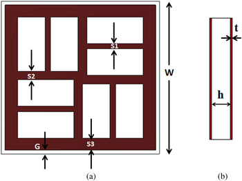
The front view of the proposed FSS unit cell is given in Fig. 1(a). Figure 1(b) shows the side view of the FSS. The proposed unit-cell design is placed on both sides of a single-layer FR4 dielectric substrate of thickness h = 1.6 mm which has relative permittivity (ε r ) of 4.3 and loss tangent (δ) of 0.025. The values of the design parameters are given in Table 1.
(a) Front view of the proposed unit cell. (b) Side view of the proposed FSS unit cell.

Unit-cell design parameters.

III. EVOLUTION OF THE UNIT CELL
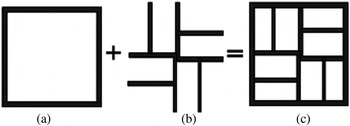
The fundamental square-loop unit cell is taken as the basic element for constructing the unit cell [Reference Kushwaha, Kumar, Ram Krishna and Oli9]. In addition, the offset crossed dipole along with an additional arm is used. The unit cell is evolved by adding the square-loop element and modified offset crossed dipole as shown in Fig. 2.
Evolution of unit cell (a) square loop, (b) modified offset crossed dipole, and (c) proposed unit cell.

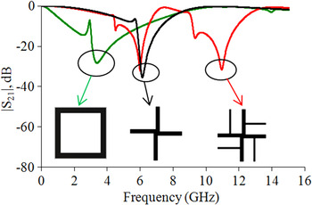
The transmission characteristics for various stages of the unit cell are given in Fig. 3. When the square loop alone is present on either side of the substrate, it provides 20 dB attenuation for 1.12 GHz bandwidth from 3.08 to 4.2 GHz centerd at 3.64 GHz. The modified offset crossed dipole provides dual resonances at 6 and 11 GHz with the bandwidth of 0.4 and 1.71 GHz respectively at the 20 dB attenuation level. It is evident from Fig. 3 that the outermost square loop controls the lower cut-off frequency and the modified offset crossed dipole is responsible for dual-band operation. The two elements are integrated and placed on both sides of the FR4 substrate to obtain the proposed UWB FSS unit cell.
Transmission characteristics of the square loop, offset crossed dipole, and modified offset crossed dipole.

IV. RESULTS AND ANALYSIS
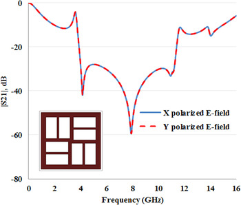
The proposed FSS placed on either side of the substrate provides the simulated transmission characteristics as in Fig. 4. The FSS provides 20 dB attenuation for a wide bandwidth of 7.53 GHz from 3.87 to 11.4 GHz.
Transmission characteristics of the proposed FSS.

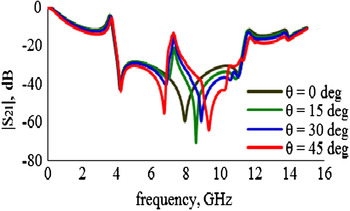
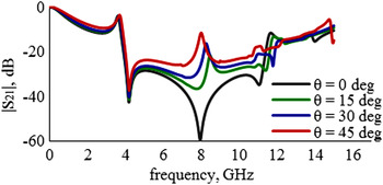
The bandwidth offered by the FSS is 98.68% with respect to the center frequency of 7.63 GHz. It is apparent that the proposed FSS provides similar transmission characteristics for X-polarized electric field (TE mode) and Y-polarized electric field (TM mode) thus exhibiting polarization independency. To test the angular stability of the proposed FSS, simulation is carried out for different angles of incidence θ = 0°, 15°, 30°, and 45°. As illustrated in Figs 5 and 6, the proposed FSS provides stable response for both TE and TM modes of polarization and the attenuation level is found to be greater than 20 dB in the desired UWB range for normal incidence. While increasing θ up to 45°, a notch is formed at 7 and 8 GHz in TE and TM modes respectively which is attributed to the double-side printed FSS [Reference Syed, Ranga, Matekovits, Esselle and Hay4]. However, it provides an attenuation of more than 11.5 dB for a wideband from 4 to 14 GHz thus exhibiting angular independency.
TE mode transmission characteristics.

TM mode transmission characteristics.

V. PARAMETRIC ANALYSIS
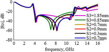
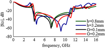
Parametric analysis has been carried out to find the optimal FSS design parameters to provide wide rejection bandwidth. The permittivity and thickness of the dielectric substrate plays an important role in designing UWB FSS. In the proposed UWB FSS unit cell, the parameters S1, S2, and S3 correspond to various widths of the strip lines. The change in response of the FSS is obtained for various values of S1, S2, and S3 as in Fig. 7. It is observed that the band stop response of the proposed FSS can be controlled by changing S1, S2, and S3 values. The optimized values of S1 = 0.5, S2 = 0.8, and S3 = 1.15 mm are considered for demonstrating the operation of the proposed FSS unit cell. Similarly the gap (2 × G) between two unit cells has the bandwidth improving capability [Reference Munk1]. The transmission characteristic of the FSS for various values of G and h is given in Fig. 8. The bandwidth achieved when G = 0.1 mm is 101.98% which is almost 3.5% more than the bandwidth obtained when G = 0.15 mm. The gap is limited to 0.15 mm due to fabrication constraints. By increasing the substrate thickness “h”, attenuation and bandwidth gets improved [Reference Costa, Genovesi and Monorchio5] which is observed from Fig. 8. If the “h” value is increased from h = 1.6 to h = 3.2 mm, attenuation bandwidth is increased by 2%. Because of the effect of increased weight and bulky size, the thickness is limited to 1.6 mm. The parameter “W” decides the unit-cell dimension, which should be of the order of sub-wavelengths to prevent the onset of grating lobes [Reference Parker and El Sheikh12–Reference Sundarsingh, Velan, Kanagasabai, Sarma, Raviteja and Alsath14] and also it controls the bandwidth of the FSS [Reference Munk1].
Transmission characteristics for various values of S1, S2, and S3.

Transmission characteristics for various values of h and G.

VI. MEASUREMENT SETUP AND MEASURED RESULT
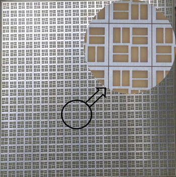
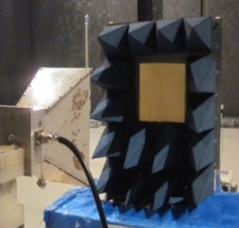
To measure the transmission characteristics of the proposed FSS, the FSS of dimensions W = 14, t = 0.035, S1 = 0.5, S2 = 0.8, S3 = 1.15, and G = 0.15 mm is fabricated. The prototype fabricated on the FR4 substrate given in Fig. 9 has 22 × 22 unit cells and the total size of the FSS screen is 31 × 31 cm2. The fabricated prototype is placed in between two horn antennas of operating range 2 to 18 GHz, separated by a distance of 2 m for the measurement as in Fig. 10. The entire test setup is surrounded by reflection absorbing material to provide scattering and reflection-free measurement.
Fabricated prototype.

Measurement setup.

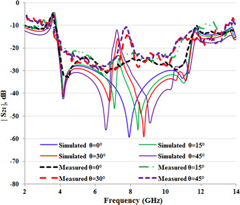
The measured transmission characteristics are compared with simulated results in Fig. 11. It is observed that simulated and measured results are in agreement with each other. For the normal incidence, 20 dB attenuation is observed for a wide bandwidth of 7.5 GHz. Also for the oblique incidences, the proposed FSS provides more than 11 dB attenuation for a wideband from 4 to 14 GHz.
Comparison of simulated and measured transmission characteristics.

VII. CONCLUSION
In this paper, a single-layer polarization-independent UWB FSS is discussed. The proposed design offers 20 dB attenuation for a wide bandwidth of 7.53 GHz in the normal incidence of the EM field. The UWB FSS provides the advantage of polarization and angular-independent operation. The simulated transmission characteristic is validated by experimental results. The proposed FSS with its wideband attenuation finds application in wideband shielding and also for performance enhancement of UWB antennas.
 Ramprabhu Sivasamy is currently a research scholar at Anna University, Chennai, India. He serves as an Assistant Professor in the Department of Electronics and Communication Engineering at Sri Sivasubramaniya Nadar College of Engineering, Kalavakkam, Chennai, Tamilnadu, India. His research interests include Frequency Selective Surfaces, Electromagnetic Shielding, Microwave Engineering, and Transmission Lines.
 Balaji Moorthy is currently pursuing his Master's degree in Engineering in Communication Systems in College of Engineering Guindy, Anna University, Chennai, India. His areas of interest include Antenna Design and Frequency Selective Surfaces.
 Malathi Kanagasabai is currently serving as an Associate Professor in the Department of Electronics and Communication Engineering, College of Engineering Guindy, Anna University, Chennai, India. Her research interests include Microwave Communication, Planar Transmission Lines, Planar Antennas, and Signal Integrity Analysis in High-Speed Systems.
 Jithila V. George is currently pursuing her Master's degree in Engineering in Communication Systems, in College of Engineering Guindy, Anna University, Chennai, India. Her areas of interest include Microwave Devices and Design of Vivaldi Antennas.
 Livya Lawrance is currently pursuing her Master's degree in Engineering in Communication Systems, in College of Engineering Guindy, Anna University, Chennai, India. Her areas of interest include Microwave Devices, Design of Grid Array Antennas, and Automotive Antennas.
 Dinesh Babu Rajendran is currently pursuing his Master's degree in Engineering in Communication Systems in College of Engineering Guindy, Anna University, Chennai, India. His areas of interest include Microwave Devices and Antenna Design.