I. INTRODUCTION
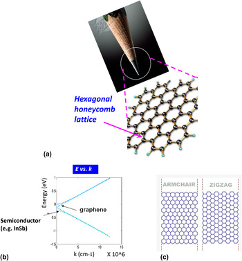
Over the centuries, new materials have formed the backbone in shaping the landscape of technology from the Si transistor to the use of light-weight, flexible displays enabled by organic polymers, for example. In this regard, graphene, a single sheet of carbon atoms arranged in a hexagonal honeycomb lattice, has catapulted science and technology to unimaginable new heights in a relatively short period of time since it was isolated from parent graphite in 2004. Reference Novoselov, Geim, Morozov, Jiang, Zhang, Dubonos, Grigorieva and Firsov1 Graphene's two surfaces and the absence of a bulk, as shown in Fig. 1(a), make it the thinnest material known and yet this membrane-like material is 5x stronger than steel owing to the strong in-plane π and σ bonds; interestingly, graphite has been known to us for centuries in the form of the common lead pencil as depicted in Fig. 1(a). Graphene exhibits a high electron mobility >200,000 cm2/V-s at room temperature and a high thermal conductivity of 5 × 10³ W/m-K. It also has an exceptional ability to carry ultra-high current densities ∼1 × 10⁹ A/cm2. Graphene has stirred a great deal of excitement for a wide range of applications that are enabled from its remarkable properties, such as rf transistors, Reference Lin, Dimitrakopoulos, Jenkins, Farmer, Chiu, Grill and Avouris2,Reference Wu, Jenkins, Valdes-Garcia, Farmer, Zhu, Bol, Dimitrakopoulos, Zhu, Xia, Avouris and Lin3 interconnects, Reference Khatami, Li, Xu and Banerjee4 ultra-capacitors, Reference Jeong, Lee, Shin, Choi, Shin, Kang and Choi5 biosensors, Reference Lu, Lerner, Qi, Mitala, Lim, Discher and Johnson6 stretchable electronics, Reference Kim, Zhao, Jang, Lee, Kim, Kim, Ahn, Kim, Choi and Hong7 thermo-electrics, Reference Wei, Bao, Pu, Lau and Shi8 photo-voltaics, Reference Miao, Tongay, Petterson, Berke, Rinzler, Appleton and Hebard9,Reference Dang, Yi, Ham, Qi, Yun, Ladewski, Strano, Hammond and Belcher10 optical applications and plasmonics, Reference Vakil and Engheta11 as well as in nano-electro-mechanical-systems. Reference Loh and Espinosa12 Needless to say, graphene has served as a model two-dimensional (2D) system that has captured the interest of researchers from a diverse array of fields spanning physics, chemistry, materials science, and engineering.
(a) Crystal structures of 2D graphene, which is a single layer of carbon atoms derived from parent graphite. The graphene lattice is a hexagonal honeycomb arrangement of carbon atoms. The lead pencil, which has been used for centuries, is composed of 3D graphite. (b) E–k diagram for pristine graphene shows that it does not possess an intrinsic band gap unlike typical semiconductors (e.g., InSb shown here), which exhibit a spectral gap. (c) GNR exhibiting the arm-chair and zigzag chirality. It is difficult to maintain pristine edges in forming GNRs through commonly used nanofabrication techniques.

While graphene has been shown to exhibit exceptional promise for a wide range of applications, its lack of a band gap as illustrated by the E–k diagram in Fig. 1(b) poses concerns for its attractiveness in some applications, particularly digital electronics where high ON/OFF ratios are desired (∼106). Although one approach for inducing a band gap in graphene is through quantum confinement by creating graphene nanoribbons (GNRs), Reference Li, Wang, Zhang, Lee and Dai13 as shown in Fig. 1(c) with widths typically <10 nm, the band gaps nonetheless are small (<few hundred meV), and it is challenging to maintain pristine edge chirality due to defects that are induced during the nanofabrication of such ribbons. Other techniques to induce band gaps utilize chemical functionalization, Reference Balog, Jorgensen, Nilsson, Andersen, Rienks, Bianchi, Fanetti, Lægsgaard, Baraldi, Lizzit, Sljivancanin, Besenbacher, Hammer, Pedersen, Hofmann and Hornekær14 and the application of an electric field in bilayer graphene. Reference Zhang, Tang, Girit, Hao, Martin, Zettl, Crommie, Shen and Wang15 In the latter case, the gaps are still less than 400 meV and the voltages required are well in excess of 100 V, which limits graphene's use in low-power devices and circuits. In general, the methods used to induce a band gap in graphene generally compromise the high mobilities that pristine graphene has to offer, while at the same time increasing process complexity.
At the same time, the development of novel characterization tools and the ability to manipulate monolayer thin graphene layers into novel device architectures have opened possibilities for the exploration of other monolayer-thin 2D crystals. Reference Novoselov, Jiang, Schedin, Booth, Khotkevich, Morozov and Geim16 Such 2D layered crystals appear to have distinct and useful properties complementing those of graphene, and the focus thus far has primarily been on inorganic material systems. Examples of such 2D layered materials include hexagonal boron nitride (h-BN), transition metal dichalcogenides, transition metal oxides, and topological insulators. Reference Wang, Kalantar-Zadeh, Kis, Coleman and Strano17,Reference Xu, Liang, Shi and Chen18 Other traditionally nonlayered structures such as germananes Reference Bianco, Butler, Jiang, Restrepo, Windl and Goldberger19 (atomic layers containing germanium) and silicenes Reference Vogt, Padova, Quaresima, Avila, Frantzeskakis, Asensio, Resta, Ealet and . Lay20 (atomic layers of silicon) have also been reported. In addition, a wide composition range between the boron–carbon–nitrogen system, Reference Song, Liu, Reddy, Narayanan, Taha-Tijerina, Peng, Gao, Lou, Vajtai and Ajayan21 and other complex multicomponent systems such as mica, and talc derived from alumina–silicate layers, also exhibit a graphite-like layered structure.
It is interesting to note that while carbon-based nanomaterials, such as three-dimensional (3D) graphite and diamond, 2D graphene, quasi one-dimensional (1D) carbon nanotubes (CNTs), GNRs and nanofibers, and zero-dimensional fullerene spheres, have captured the attention of researchers for several decades now, these materials are all derived from a single element on the periodic table, namely carbon arranged in various structural forms. On the other hand, the wide range of compositions of other 2D layered materials span the periodic table and one can expect to see a rich and exciting spectrum of structures and properties. For example, h-BN and HfS2 are insulators, while NbSe2, a transition metal dichalcogenide is metallic, and monolayers of other transition metal dichalcogenides such as MoS2, WS2, and WSe2 are direct band gap semiconductors. The rich variety of properties that 2D layered material systems offer creates exciting prospects for their device applications in electronics, sensing, photonics, catalysis, bioengineering, energy harvesting, and flexible electronics. 22 This paper provides an overview of 2D layered nanomaterials, which are poised to play an important role for enabling innovative and exciting applications over the coming years.
II. NONGRAPHENE 2D LAYERED CRYSTALS
The research activity in this emerging and interdisciplinary area will greatly benefit from the knowledge and infrastructure that has been established for graphene over the past decade. Devices constructed from 2D materials offer potential advantages due to the interesting properties these materials possess, which arise from their structural attributes that are discussed in Sec. II. A. This is followed by a more detailed description in Sec. II. B of the possible application areas these materials are likely to impact in the future. Finally, recent progress made in the synthesis of these materials is discussed in Sec. II. C.
A. Structure and properties
A host of 2D layered crystals are known, which include the transition metal dichalcogenides, Reference Wilson and Yoffe23 transition metal oxides, Reference Osada and Sasaki24 and nitrides. Reference Dean, Young, Meric, Lee, Wang, Sorgenfrei, Watanabe, Taniguchi, Kim, Shepard and Hone25 Needless to say, such material systems push the limits of vertical scaling. In particular, the transition metal dichalcogenides exhibit a wide range of electronic, optical, mechanical, chemical, and thermal properties and have been known to us in their bulk form for decades.
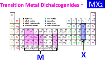
The transition metal dichalcogenides consist of hexagonal layers of metal M atoms [from group 4B (e.g., Ti, Zr, Hf), group 5B (e.g., V, Nb, Ta) or group 6B (e.g., Mo, W), group 7B (e.g., Tc, Re), and group 10B (e.g., Pd, Pt)], which are sandwiched between two layers of chalcogen atoms X (S, Se or Te) with stoichiometry MX2; the structural arrangement of this is shown for the case of MoS2 in Fig. 2, where M = Mo and X = S. As with transition metal dichalcogenides and many of the other layered material systems, the intralayer bonding is primarily due to the strong covalent in-plane bonding between the atoms, but the interlayer bonding is governed by the weaker van der Waals interaction. In fact, it is this weak van der Waals interaction that is responsible for the ease with which these materials can be mechanically cleaved through exfoliation into individual layers. Depending on the combination of the transition metal atom and the chalcogen atom, a wide variety of transition metal dichalcogenides are possible, as illustrated in Fig. 3, each offering a unique set of properties.
Crystalline structure of layered MoS2 where the Mo atom is sandwiched between the S atom. Although the intralayer bonding is through the strong covalent interaction, the interlayer bonding occurs via the weak van der Waals interaction. Unlike graphene, monolayers of MoS2 exhibit a large and inherent band gap ∼1.8 eV and it is also a direct-band gap semiconductor. Reprinted with permission from Ref. Reference Radisavljevic, Radenovic, Brivio, Giacometti and Kis44, Copyright © Macmillan Publishers Ltd: Nature (2011).

The transition metal dichalcogenides are an example of 2D layered materials. Depending on the combination of the transition metal M and the chalcogen atom X (S, Se, Te), a wide range of properties can arise.

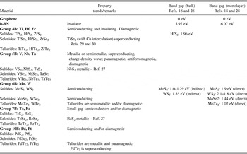
Such properties have been deduced theoretically using first principles density functional theory to compute the band structures of these materials. While 88 combinations of MX2 compounds are possible, these calculations show that only about 44 of these are stable in their monolayer form. Reference Ataca, Sahin and Ciraci26 Their properties range from semiconducting, metallic, semimetallic, ferromagnetic, or superconducting depending on the atomic coordination of the transition metal and the number of electrons in the d-band. In going from group 4B elements (Ti, Zr, Hf) of the periodic table to group 10B (Pd, Pt) elements, the nonbonding d-bands of the transition metal are progressively filled, which has an impact on their ensuing properties. To illustrate this, the d-bands in NbSe2 and ReS2 are not fully occupied, which lend them their predominantly metallic character. Reference Kuc, Zibouche and Heine27 In contrast, when the d-bands are completely filled, the materials exhibit semiconducting (e.g., MoS2 and PtS2) and, in some cases, insulating (e.g., HfS2) characteristics. Reference Chhowalla, Shin, Eda, Li, Loh and Zhang28 In other cases, superconductivity has also been observed in layered MX2 materials such as TiSe2 through Cu intercalation. Reference Morosan, Zandbergen, Dennis, Bos, Onse, Klimczuk, Ramirez, Ong and Cava29,Reference Husanikova, Fedor, Derer, Soltys, Cambel, Iavarone, May and Karapetrov30 It is interesting to note that as we traverse down the Group 6 chalcogen atoms, the d-bands become increasingly diffuse, and this spreading of the bands reduces the band gap of the semiconducting MX2 materials in going from the smaller atomic number element S to the larger atomic number element Te; for example, MoS2 has a band gap of ∼1.3 eV, while MoTe2 has a lower band gap of ∼1.0 eV. Reference Wilson and Yoffe23
While the properties of the broad class of 2D layered materials are diverse and interesting in the bulk, progress in isolating single layers of sp 2-bonded graphene from bulk graphite has led to similar findings, which suggest monolayers of nongraphene 2D layered materials may also have unique properties that differ from the bulk. Reference Li and Galli31 For example, in exfoliating single layers of MoS2 from bulk MoS2 crystal, the absence of the sp z orbital interaction between adjacent MoS2 layers causes the band gap to widen through quantum confinement effects. Besides the increase in band gap, this change in orbital hybridization turns single-layer MoS2 from an indirect-band gap semiconductor to a direct band gap semiconductor. This indirect-to-direct band gap transition has also been predicted theoretically for other MX2 materials such as WS2, which has a bulk indirect band gap of 1.3 eV, while monolayers are direct band gap semiconductors with a band gap of 2.1 eV. Reference Kuc, Zibouche and Heine27 The selenides of tungsten, Reference Zhao, Ghorannevis, Chu, Toh, Kloc, Tan and Eda32 as well as the monolayers of MoSe2 and MoTe2, show similar characteristics. Reference Ma, Dai, Guo, Niu, Lu and Huang33 Table I provides a summary of the general properties and the band gap values for a number of layered materials.
Example layered materials and their general properties.

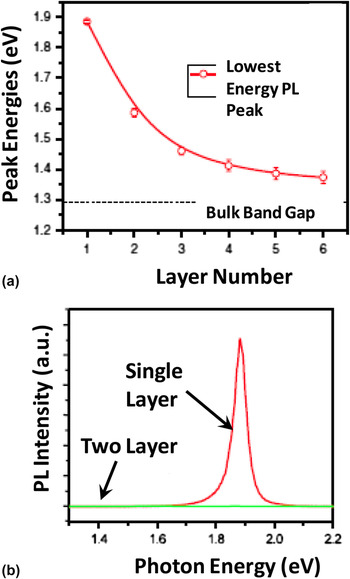
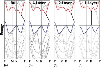
Experimentally, photoluminescence has emerged as a key technique to confirm this quantum confinement induced indirect-to-direct band gap transition in some monolayer 2D d-electron material systems, such as MoS2 and MoSe2. In the case of MoS2, the photoluminescence peak is the strongest for monolayers [Figs. 4(a) and 4(b)], and the height of the peak weakens as the number of layers increases, as shown in Fig. 4(a). Reference Splendiani, Sun, Zhang, Li, Kim, Chim, Galli and Wang34,Reference Mak, Lee, Hone, Shan and Heinz35 Band structure calculations of MoS2, as depicted in Fig. 5, illustrate the indirect nature of the electron transitions from the bulk [Fig. 5(a)], 4-layer [Fig. 5(b)], and bilayer [Fig. 5(c)] MoS2, where the valence band maximum lies at the Γ point, while the conduction band minimum lies half-way between the Γ–Κ line. Reference Splendiani, Sun, Zhang, Li, Kim, Chim, Galli and Wang34 In contrast, the valence band maximum and the conduction band minimum line up at the Κ-point for monolayer MoS2 [Fig. 5(d)], validating its direct gap semiconducting characteristics, as seen experimentally [Fig. 4(b)]. Reference Mak, Lee, Hone, Shan and Heinz35
(a) Experimental results showing the intensity of the lowest energy photoluminescence peak decreasing with layer number. (b) Monolayers of MoS2 show a pronounced photoluminescence peak, which is not evident in bilayer MoS2, indicative of an indirect-to-direct band gap transition for monolayer MoS2. Reprinted with permission from Ref. Reference Mak, Lee, Hone, Shan and Heinz35. Copyright © The American Physical Society: Phys. Rev. Lett., 2010.

Band structure calculations for MoS2 show that the conduction band minimum lies half-way between the Γ–K line while the valance band maximum is at the Γ point for (a) bulk, (b) 4-layer, and (c) bilayer MoS2. (d) For monolayer MoS2, the conduction band minimum and the valence band maximum line up at the K point, confirming the direct band gap transition that is observed experimentally. Reprinted with permission from Ref. Reference Splendiani, Sun, Zhang, Li, Kim, Chim, Galli and Wang34, Copyright © The American Chemical Society: Nano Lett. (2010).

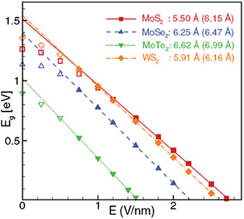
Besides this observed band gap transition from indirect-to-direct gap, it is also interesting to note that the band gaps in some bilayer MX2 materials can be tuned through the application of an external electric field. For example, density functional theory calculations conducted on bilayer MoS2, WS2, MoSe2, and MoTe2 show that their band gaps undergo a gradual semiconducting-to-metallic transition through the application of an external electric field oriented orthogonal to the plane of the layers. Reference Boker, Severin, Muller, Janowitz, Manzke, Voss, Kruger, Mazur and Pollmann36,Reference Klein, Tiefenbacher, Eyert, Pettenkofer and Jaegermann37 While similar observations have been made in bilayer graphene, the range of tunability in graphene is much lower. The critical electric field for this semiconductor-to-metal transition decreases with increasing atomic number of the chalcogen atom, i.e., in going from S, Se to Te (Fig. 6). For example, the critical field for MoTe2 is found to be the lowest (1.5 V/nm), followed by MoSe2 (2.2 V/nm), while the highest critical field is seen for MoS2 (2.7 V/nm). This interesting trend has been attributed to the increasingly diffuse nature of the valence p z orbitals of the chalcogen atoms with increasing atomic number, which makes charge transfer from the chalcogen atom to Mo easier under the same electric field. Reference Ramasubramaniam, Naveh and Towe38
Results of band gap tuning with an externally applied electric field for various MX2 materials. The semiconductor-to-metal transition occurs within a range of E-field from 1.5 to 2.8 V/m for the materials shown. Reprinted with permission from Ref. Reference Ramasubramaniam, Naveh and Towe38, Copyright © The American Physical Society: Phys. Rev. B (2011).

Low temperature phenomena such as superconductivity and charge density wave effects have also been observed in some MX2 compounds such as NbSe2 and TaS2 and Cu-intercalated TiSe2. Reference Morosan, Zandbergen, Dennis, Bos, Onse, Klimczuk, Ramirez, Ong and Cava29,Reference Husanikova, Fedor, Derer, Soltys, Cambel, Iavarone, May and Karapetrov30 Besides the transition metal dichalcogenides, the chalcogenides of group III (GaSe, GaTe, InSe), group IV (GeS, GeSe, SnS, SnSe), and group V (Bi2Se3, Bi2Te3) also show a graphite-like layered structure and have prospects in electronics, photonics, and energy harvesting; incidentally, Bi2Se3 and Bi2Te3 are also topological insulators, besides being common thermoelectric materials in the bulk.
In addition, ab initio calculations conducted on other single-element materials such as Si suggest the similarity of sp 2 bonded 2D silicon—silicene—to graphene, which also exhibits a linear dispersion relationship near the K point, just like graphene. Reference Lebegue and Eriksson39 These theoretical calculations also show that planar 2D silicon appears to be unstable and that a buckled morphology for silicene seems to be energetically more favorable. Driven by the success of graphene research, interest in silicene continues to grow, but only a few experimental reports have appeared, which have verified the presence of silicene on Ag(111) substrates through scanning tunneling microscopy and angular-resolved photoemission spectroscopy investigations. Reference Vogt, Padova, Quaresima, Avila, Frantzeskakis, Asensio, Resta, Ealet and . Lay20
While 2D layered materials exhibit a range of exciting properties as discussed, certain key issues, such as the role of doping, contacts and strain, are discussed in more detail here, due to the impact these have for enabling practical device applications to emerge from such materials.
The ability to control the doping of semiconducting 2D layered materials to selectively form p- and n-type regions is a necessary requirement to realize complimentary logic circuits. Besides selectively doping n-type and p-type regions in the same parent semiconductor, forming lateral heterostructures of dissimilar materials, similar to recent work with graphene and h-BN, Reference Levendorf, Kim, Brown, Huang, Havener, Muller and Park40 suggests prospects for the realization of other 2D lateral n-type and p-type heterostructures. Vertical heterostructures of alternate n-type and p-type semiconductors are another possibility for forming such p–n junctions. In all such proposed schemes, the issues to be resolved include identifying the appropriate substrates, where both the n-type (e.g., MoS2) and p-type (e.g., WSe2) semiconductors can be synthesized laterally or as vertical heterostructures. While the transfer of the parent 2D material onto a target substrate is one possible avenue, this approach introduces added process complexities, in addition to potential defects.
Another important factor to consider is the role contacts play in determining the device performance of the 2D layered materials for transistor applications for example, as has been the case for Si devices, Reference Landman, Barnett, Scherbakov and Avouris41 or nanocarbon materials. Reference Leonard and Talin42,Reference Nemec, Tomanek and Cuniberti43 While bulk MoS2 is seen to exhibit a relatively high carrier mobility, the observed electron mobility in single-layer MoS2 is unexpectedly low. Reference Novoselov, Jiang, Schedin, Booth, Khotkevich, Morozov and Geim16,Reference Radisavljevic, Radenovic, Brivio, Giacometti and Kis44 This has been attributed to the Au contact to the 2D semiconducting MoS2, where a tunnel barrier results at the Au-MoS2 interface and suppresses electron injection into MoS2. Reference Popov, Seifert and Tomanek45 Popov et al. Reference Popov, Seifert and Tomanek45 suggest that the low mobility of monolayer MoS2 field-effect-transistors (FETs) may have more to do with an inappropriate choice of contacts and may not necessarily be due to the presumed low mobility of the monolayer MoS2 itself. Theoretical ab initio density functional calculations have yielded insights that suggest Ti as an appropriate contact material for monolayer MoS2 in contrast to Au. Reference Popov, Seifert and Tomanek45 The low work function of Ti, coupled with its d-electron orbitals, suggests that it mixes favorably with the 4d states of Mo, making it a suitable, low-resistance ohmic contact for MoS2. Clearly, finding appropriate materials to serve as contacts to semiconducting 2D layered materials will be an active area of research for enabling high-performance devices in the future.
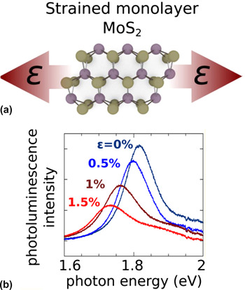
It is also remarkable to note the strong influence that mechanical strain has on the band gap of some 2D layered semiconducting materials. Reference Conley, Wang, Ziegler, Haglund, Pantelides and Bolotin46–Reference Scalise, Houssa, Pourtois, Afanasev and Stesmans49 This is especially attractive in the case of MoS2, which has an in-plane strength comparable to that of steel and has the ability to accommodate strains well in excess of 11% without showing signs of mechanical degradation. Reference Bertolazzi, Brivio and Kis50 In general, strain in semiconductors modifies the lattice constant and crystal symmetry [Fig. 7(a)], Reference Conley, Wang, Ziegler, Haglund, Pantelides and Bolotin46 causing the energy bands to shift, which in turn induces changes in the relative effective masses. Reference Sanchez-Perez, Boztug, Chen, Sudradjat, Paskiewicz, Jacobson, Lagally and Paiella51 Specifically, the band structure of monolayer and bilayer MoS2 appears to be strongly perturbed under uniaxial tensile strain up to 2.2%, where Raman spectroscopy and photoluminescence measurements were conducted in situ. Reference Conley, Wang, Ziegler, Haglund, Pantelides and Bolotin46 The optical band gap was found to decrease at a rate of ∼45 and ∼120 meV/% of strain for monolayer and bilayer MoS2, respectively. In addition, at an applied strain of ∼1%, the photoluminescence intensity decreased, which is suggestive of a strain-induced direct-to-indirect band gap transition for monolayer MoS2, as shown in Fig. 7(b). Reference Conley, Wang, Ziegler, Haglund, Pantelides and Bolotin46
(a) The atomic crystal lattice displacements shown pictorially for monolayer MoS2 under strain. (b) The induced strain in some 2D materials, e.g., MoS2, has the effect of changing the optical properties from direct band gap to indirect with an applied strain as low as 1%. Reprinted with permission from Ref. Reference Conley, Wang, Ziegler, Haglund, Pantelides and Bolotin46, Copyright © The American Chemical Society: Nano Lett. (2013).

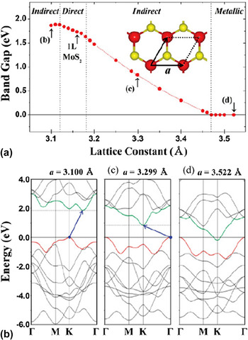
Theoretical calculations on the role of strain in MoS2, MoSe2, MoTe2, WS2, WSe2, and WTe2, indicate that the properties of these materials are sensitively dependent on strain, where the semiconducting direct band gap characteristics can be transformed to metallic under certain strain ranges. Reference Yun, Han, Hong, Kim and Lee52 For example, the unstrained lattice constant of MoS2 is 3.16 Å, and the direct band gap characteristics, which is seen for strains from −1.3% to 0.3%, undergoes an indirect band gap transition [e.g., point c in Fig. 8(a)] metallic transition for strains close to 10% [e.g., point d in Fig. 8(a)]. The corresponding calculated band structures for the various strain levels are shown in Fig. 8(b). These early reports clearly suggest the potential for strain engineering to modify band gaps, carrier effective masses and mobilities, to yield a number of interesting tunable devices. Reference Feng, Qian, Huang and Li53
Theoretical calculations show the effect of compressive and tensile strain on the optical and electronic properties of monolayer MoS2. (a) The lattice constant for unstrained MoS2 is 3.16 Å. Direct band gap characteristics are present for a strain in the range of −1.3%–0.3%. For strains larger than this, an indirect band gap transition (e.g., point c) is seen that transitions to a metallic state for strains close to 10% (e.g., point d). (b) The corresponding calculated band structures, which illustrate the changes in band gap occurring at various strain-levels, where changes in curvature also impact the electron and hole effective masses. Reprinted with permission from Ref. Reference Yun, Han, Hong, Kim and Lee52. Copyright © The American Physical Society: Phys. Rev. B (2012).

In addition, the ability to stack dissimilar 2D atomic layers into 3D super-lattices and heterostructures offers exciting prospects for enabling new physics to emerge that couples electronic, optical, thermal, mechanical and related properties into a single platform. Such artificially engineered van der Waals solids should open up a new paradigm to enable new vistas in device possibilities that would otherwise be unimaginable. In fact, recent experimental reports on the vertical integration of heterostructures of 2D layered materials have already led to demonstrations of novel physics and innovative devices to emerge from such structures. As one example, Yu et al. Reference Yu, Liu, Zhou, Yin, Li, Huang and Duan54 formed heterostructures of graphene and MoS2, where they reported high-efficiency photocurrent generation from such 2D layered vertical heterostructure junctions. Through the integration of graphene-based single or dual gates below and above the vertical heterostructures, the amplitude and polarity of the photocurrent in the vertical heterostructures was tuned by the external graphene gate. The concomitant external and internal quantum efficiency was demonstrated to be 55% and 85%, respectively, suggesting that the photocarrier generation, separation, and transport processes can be successfully controlled by the application of an external electric field in such vertical heterostructures of 2D layered materials.
In earlier work on heterostructures, 2D layered materials such as h-BN and MoS2 have served as tunneling barrier layers between graphene electrodes, which yielded a vertical bipolar FET. Reference Britnell, Gorbachev, Jalil, Belle, Schedin, Mishchenko, Georgiou, Katsnelson, Eaves, Morozov, Peres, Leist, Geim, Novoselov and Ponomarenko55 The tunneling time for electrons to traverse the nanometer-thick barrier was demonstrated to be extremely small in the range of femtoseconds, which far exceeds the switching frequency of conventional planar FETs and provides a promising example for the potential of 2D heterostructures for beyond-CMOS architectures. Vertical field-effect tunneling devices have also been constructed with such heterostructures, where a 2D WS2 barrier layer was used with graphene, and a very high ON-state current was demonstrated at room temperature for devices formed on transparent and flexible substrates. Reference Georgiou, Jalil, Belle, Britnell, Gorbachev, Morozov, Kim, Gholinia, Haigh, Makarovsky, Eaves, Ponomarenko, Geim, Novoselov and Mishchenko56
Vertical heterostructures of semiconducting MX2 materials with graphene have also shown to be photoactive, where an incoming photon generates electron–hole pairs within the band gap of the semiconducting MX2 material. The electron–hole pairs are then separated at a p–n junction and extracted as a photocurrent from the highly conducting and transparent graphene electrodes formed on flexible substrates. Reference Britnell, Ribeiro, Eckmann, Jalil, Belle, Mishchenko, Kim, Gorbachev, Georgiou, Morozov, Grigorenko, Geim, Casiraghi, Castro Neto and Novoselov57 For example, with a graphene-WS2-graphene trilayer, a photoresponsivity >0.1 A/W was achieved experimentally, which corresponded to an external quantum efficiency of above 30%. Despite the fact that the layers are only a few monolayers thick, ab initio calculations of WS2, WSe2, and MoS2 show critical points or strong peaks to arise in the electronic density of states of these materials in the visible range. These critical points in the electronic density of states, also known as Van Hove singularities, lead to an enhancement in optical absorption. Interestingly, Van Hove singularities have also been observed in 1D materials, such as single-walled CNTs but are not present in 3D materials since the density of states is continuous in the latter case. The unique manner in which the d-orbitals of the transition metal combine with the p-orbitals of the chalcogen atom to form the valence and conduction bands leads to highly localized electronic bands that result in the Van Hove singularities in the density of states of these materials. Britnell et al. Reference Britnell, Ribeiro, Eckmann, Jalil, Belle, Mishchenko, Kim, Gorbachev, Georgiou, Morozov, Grigorenko, Geim, Casiraghi, Castro Neto and Novoselov57 also demonstrated that besides the presence of Van Hove singularities, the efficiency for electron–hole pair generation in these 2D heterostructures was enhanced by an order of magnitude with the incorporation of plasmonic gold nanoparticles on the 2D surface.
In other recent work on vertical heterostructures, MoS2 and amorphous-silicon (a-Si) vertical stacks were used to create a photodetector Reference Esmaeili-Rad and Salahuddin58 that exhibited a rise and fall time of about 0.3 ms, making it roughly 10x faster compared to a-Si devices. Such examples present a convincing case for new physics to emerge in 2D vertical heterostructures that has the potential to open up interesting avenues for enabling innovative electronic, photonic, energy harvesting, sensing and other related devices.
At the same time it is also clear that the need for high-quality, defect-free materials, the importance of basic science and discovery for creating a library of new 2D crystals with exciting properties, and for developing processes that enable easy integration of such thin atomic layers into device architectures will be areas of great importance in the future research of 2D materials. The challenges of synthesizing such structures with atomically smooth interfaces, particularly using scalable techniques, will remain an important area of research to fully exploit the promise of these materials. In the next section, Sec. II. B, more details on specific device applications arising from such 2D layered materials are discussed, followed by an overview in Sec. II. C of the recent progress that has been made in developing synthesis techniques for forming these materials.
B. Device applications
1. Electronic devices
The 2D transition metal dichalcogenides and other 2D crystals offer properties that complement those of graphene. As mentioned, transition metal dichalcogenides such as MoS2, MoSe2, WS2, and WSe2 have an inherent and appreciable band gap that can extend the possibilities of such materials in electronics, photonics and related applications, beyond that of graphene. Reference Podzorov, Gershenson, Kloc, Zeis and Bucher59 As an example, one of the most important applications of semiconductors is in transistors for digital electronics, which continue to be driven by miniaturization and Moore's Law.
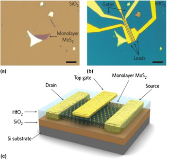
In general, 2D materials can potentially replace conventional semiconductors for ultra-scaled thin-body transistor applications given their pristine interfaces that are free of dangling bonds and where transport and scattering is confined to the plane of the material, to enable low-power and low-dissipation devices. Interestingly, electrical characterization of single-layer MoS2 FETs has shown that it is an n-type material, with a mobility of 0.5–3 cm2/V-s Reference Novoselov, Jiang, Schedin, Booth, Khotkevich, Morozov and Geim16,Reference Ghatak, Pal and Ghosh60 , which is substantially lower than the bulk mobility of MoS2. Reference Fivaz and Mooser61 Through measurements conducted at cryogenic temperatures, the electron transport in 2D layered MoS2 transistors on SiO2/Si appears to be dominated by trapped charges in the SiO2 substrate, which forms a wide band of localized states where conduction occurs through the variable range hopping mechanism and leads to carrier localization. Reference Ghatak, Pal and Ghosh60 This coulombic mechanism for scattering in 2D layered materials originates from the randomly charged impurities that lie at interfaces, and often the appropriate choice of dielectrics can enhance mobilities. Reference Debdeep and Aniruddha62–Reference Liu, Neal and Ye64 For example, while the initial monolayer MoS2 FETs were constructed using an SiO2 gate, when a high-k, top-gate dielectric such as HfO2 was used, as shown in the schematic of Fig. 9, the mobility increased to 200 cm2/V-s, Reference Radisavljevic, Radenovic, Brivio, Giacometti and Kis44 besides also possibly modifying the phonon spectrum in the top-gated MoS2 interface. These top-gated transistors from 2D monolayers of MoS2 with high-k HfO2 dielectrics showed ON/OFF ratios many orders of magnitude larger than the best graphene transistors at room temperature, Reference Radisavljevic, Radenovic, Brivio, Giacometti and Kis44 and the mobility of single-layer MoS2 devices was comparable to graphene nanoribbon devices but much lower than that of either pristine graphene or Si transistors. Reference Kim, Choi, Kim, Cho and Chung65 Theoretical calculations of mobility in monolayer MoS2 have also considered the role of deformation potentials and Frohlich interactions, Reference Kaasbjerg, Thygesen and Jacobsen66 and mobility has also been investigated as a function of temperature to shed insights into other scattering mechanisms in 2D layered materials, Reference Kim, Konar, Hwang, Lee, Lee, Yang, Jung, Kim, Yoo, Choi, Jin, Lee, Jena, Choi and Kim67 such as acoustic and optical phonon scattering, surface interface phonon scattering, and roughness scattering. Reference Wang, Kalantar-Zadeh, Kis, Coleman and Strano17
The first FET device fabricated from a single flake of MoS2, isolated in (a) and shown in (b) as a fabricated device. (c) A schematic of the transistor architecture depicts the top-gated device where a high-k material, HfO2 used as the inter-layer dielectric, enhanced the transistor performance. Reprinted with permission from Ref. Reference Radisavljevic, Radenovic, Brivio, Giacometti and Kis44, Copyright © Macmillan Publishers Ltd: Nature (2011).

Work conducted by Yoon et al. Reference Yoon, Ganapathi and Salahuddin68 using nonequilibrium Green's function quantum transport simulations, in addition to other reports, Reference Liu, Kumar, Ouyang and Guo69 suggest that MoS2 transistors appear to be well suited for low-power, low-speed applications. This assertion has largely been driven by the heavier electron effective mass (m* = 0.45m 0) and hence lower mobility of charge carriers in MoS2, in comparison to high-performance III–V materials, such as GaAs or InSb.
Combining semiconducting 2D layered materials with 2D dielectrics, such as h-BN, which is most similar in structure to graphene, allows for the design of metal/dielectric/semiconductor interfaces for heterostructure FETs or tunneling devices, as described earlier. Reference Georgiou, Jalil, Belle, Britnell, Gorbachev, Morozov, Kim, Gholinia, Haigh, Makarovsky, Eaves, Ponomarenko, Geim, Novoselov and Mishchenko56 To further elaborate on tunneling devices, it is interesting to note the impact of rotational alignment on 2D graphene-based tunneling devices, such as twisted graphene layers Reference Bistritzer and MacDonald70 and graphene-insulator-graphene junctions. Reference Feenstra, Jena and Gu71 Interestingly, in both cases, it is shown that a large resonant current peak is produced at certain relative rotational angles of the electrodes, where the coupling between the layers is treated to be spatially uniform. When the electrodes have a near perfect rotational alignment, the nonlinearity in the I–V characteristic is shown to be the strongest, although follow-up work Reference Perebeinos, Tersoff and Avouris72 seems to suggest tunneling does not necessarily get amplified at specific rotational angles. Experimentally, resonant tunneling has also been observed in h-BN/graphene heterostructure devices, Reference Britnell, Gorbachev, Geim, Ponomarenko, Mishchenko, Greenaway, Fromhold, Novoselov and Eaves73 where the ultra-fast switching times in such devices may potentially enable applications in high-frequency logic devices, although the role of rotational alignment in such heterostructures was not specifically discussed.
Beyond single devices, multiple transistor devices have also been integrated to enable digital circuits, such as inverters and NOR logic gates by patterning electrodes on a single layer of MoS2 on which the circuits are fabricated. Reference Radisavljevic, Whitwick and Kis74 Recently, complex integrated circuits built on bilayer MoS2 were also demonstrated, which included an inverter circuit and a logic NAND gate to achieve static random access memory operation. Reference Wang, Yu, Lee, Shi, Hsu, Chin, Li, Dubey, Kong and Palacios75 In addition, the scaling trends of Si transistors pushes billions of transistors in smaller and smaller areas, which poses a serious concern in mitigating heat management issues. However, through phonon engineering in the atomically sharp interfaces of 2D materials, thermal transport across interfaces can be tuned and optimized, which will play a major role in determining the performance of ultra-high-density nanoscale circuits. Thermally induced transitions in 2D layered materials also creates an interesting potential for enabling innovative device applications. For example, in work conducted by Tongay et al., Reference Tongay, Zhou, Ataca, Lo, Matthews, Li, Grossman and Wu76 a thermally induced indirect-to-direct band gap transition was observed in few-layer MoSe2 using photoluminescence, where a temperature increase drove few-layer MoSe2 toward the 2D limit. It has been hypothesized that a temperature rise in few-layer MoSe2 leads to thermal expansion, which thermally decouples adjacent layers. In contrast to MoSe2, where the indirect band gaps and direct band gaps are nearly degenerate, MoS2 on the other hand did not exhibit this indirect-to-direct band gap transition with temperature. Few-layer MoSe2 thus provides an example of a 2D layered material where the optical properties can be controlled reversibly from indirect band gap to direct band gap by modulating the external temperature, which may provide interesting prospects for device applications in the future.
2. Optoelectronic, photonic, and energy-harvesting devices
The d-orbital conductivity of the metallic components in the case of transition metal dichalcogenides makes them an interesting material system for exploring optical properties. Reference Chhowalla, Shin, Eda, Li, Loh and Zhang28 As discussed earlier, bulk MoS2 films, which have been used in the lubricant industry for many years, transform from an indirect band gap semiconductor with a band gap of ∼1.2 eV to a direct band gap semiconductor with a gap of ∼1.8 eV for single-layers. Reference Mak, Lee, Hone, Shan and Heinz35 The intrinsic band gap in these layered materials can be tuned depending on the choice of materials, varying the ratio of each of the components, and the number of layers that are present. This suggests that the optical absorbance in such materials can be engineered, which makes them particularly attractive for optoelectronics applications, including photo-detectors, lasers, and light-emission devices. Conversely, they can also be an interesting choice for light-absorbing materials in photovoltaic applications.
A phototransistor has been demonstrated from single, mechanically exfoliated layers of MoS2, which can serve as a photo detector, where the photocurrent was shown to depend on the incident light intensity. Reference Yin, Li, Li, Jiang, Shi, Sun, Lu, Zhang, Chen and Zhang77 Coupled with the fast response time, high photo-responsivity, and good stability, such devices appear to exhibit promising characteristics when compared to similar graphene devices. In addition, by using MoS2 layers of different thicknesses, photo-detection can be tuned for different wave lengths, where single- and double-layer MoS2 were shown to be effective for detecting green light, while triple-layer MoS2 was well suited for red light. Reference Lee, Min, Chang, Park, Nam, Kim, Kim, Ryu and Im78 Besides MoS2, other 2D thin films, such as WS2, have also been shown to be photosensitive, Reference Gourmelon, Lignier, Hadouda, Couturier, Bernede, Tedd, Pouzet and Salardenne79 and Table I provides examples of other optically active materials.
The 2D layered semiconductor materials are also very attractive for light emission devices, as was demonstrated recently in photoluminescence experiments. Photoluminescence is seen in monolayer MoS2, and the quantum yield of the monolayer MoS2 was measured to be much higher than for bilayer and bulk MoS2 as shown in Figs. 4(a) and 4(b). Reference Splendiani, Sun, Zhang, Li, Kim, Chim, Galli and Wang34,Reference Mak, Lee, Hone, Shan and Heinz35 However, observation of photoluminescence in 2D layered materials needs to be explored further, given that the quantum yield measured so far in MoS2 is much lower, ∼4 × 10⁻³, which is more than 2-orders of magnitude lower than that would be expected for a direct gap semiconductor. Reference Mak, Lee, Hone, Shan and Heinz35 Increasing the quantum yield in such materials by understanding the photoluminescence emission and quenching processes can increase their potential in photonic and optoelectronic devices.
Given the tunable, direct band gaps of some of the 2D transition metal dichalcogenides and their relative earth abundance, they also appear to be a promising choice for solar cells, potentially opening up prospects for multijunction solar cells that capture photons from the visible to the near-infrared. Reference Polman and Atwater80 In fact, early work conducted on some MX2 materials shows that they have large optical absorption (>107 m−1 across the visible range), which implies that 95% of the light can be absorbed by a 300-nm film. Reference Britnell, Ribeiro, Eckmann, Jalil, Belle, Mishchenko, Kim, Gorbachev, Georgiou, Morozov, Grigorenko, Geim, Casiraghi, Castro Neto and Novoselov57 Bernardi et al. Reference Bernardi, Palummo and Grossman81 have explored monolayers of MoS2, MoSe2, and WS2 and have shown that a layer as thin as 1 nm has the exceptional ability to absorb 5–10% of the incident light. When compared to conventional solar cell materials such as GaAs and Si, the absorption in some of these 2D layered materials is an order of magnitude higher. Moreover, Bernardi et al. explored two types of device architectures. The first was based on a Schottky barrier solar cell formed from heterostructures of MoS2 and graphene, and the second was an excitonic solar cell formed using heterostructures of MoS2 and WS2. Their work illustrated that despite the active layers being just 1 nm thick, they can still attain a power conversion efficiency of up to ∼1%, corresponding to approximately 1–3 orders of magnitude higher power densities than the best existing ultrathin solar cells. In addition, as discussed earlier, the strong light–matter interactions in some MX2 materials can lead to a large photon absorption, which arises from the Van Hove singularities present in these materials that can benefit solar cell applications as well. Reference Britnell, Ribeiro, Eckmann, Jalil, Belle, Mishchenko, Kim, Gorbachev, Georgiou, Morozov, Grigorenko, Geim, Casiraghi, Castro Neto and Novoselov57 The optical absorption in these 2D layered materials was further improved by the use of plasmonic gold nanospheres, as discussed earlier, Reference Britnell, Ribeiro, Eckmann, Jalil, Belle, Mishchenko, Kim, Gorbachev, Georgiou, Morozov, Grigorenko, Geim, Casiraghi, Castro Neto and Novoselov57 that were created on top of the 2D heterostructures, which yielded a 10-fold increase in the photocurrent. Similarly, interesting reports have emerged recently, which have incorporated MoS2 with organic semiconductors for the realization of hybrid bulk heterojunction solar cells, Reference Shanmugam, Bansal, Durcan and Yu82 as well as electrochemical solar cells where WS2 in combination with TiO2 acts as a promising absorber material. Reference Thomalla and Tributsch83 These preliminary reports suggest that some 2D semiconducting monolayer materials hold promise for photovoltaic applications, where such devices can potentially be formed on low-cost, transparent and flexible substrates.
3. Devices on flexible and transparent substrates
The 2D layered materials, given their atomically thin architectures, appear to be ideally suited for flexible electronics, as well as transparent substrates for optoelectronics applications. For large-area, low-cost electronics, 2D MoS2 or other 2D crystals may be an alternative to low-mobility materials such as amorphous silicon or organic semiconductors, which degrade easily with time, to enable potentially higher frequency devices on conformal and flexible substrates. Together with graphene and insulating materials such as h-BN, 2D semiconducting materials may be an attractive choice for constructing digital circuits on flexible and transparent substrates for applications such as paper-like transparent displays, wearable electronics, and solar cells.
In addition, the mechanical properties of MoS2 also appear to be very attractive given the strong intralayer covalent bonds; the in-plane strength of MoS2 has been found to be 30 times larger than steel, where a Young's modulus of 270 GPa was measured. Reference Bertolazzi, Brivio and Kis50 In general, the unique combination of high-strength, excellent out-of-plane flexibility, low broadband absorption, and outstanding and diverse electronic properties, 2D materials of nitrides, oxides, and sulfides can be envisioned as promising earth-abundant materials for components in flexible and transparent electronic applications, where conductors, semiconductors, and dielectrics are needed.
C. Synthesis approaches for 2D layered systems
Synthesis of high-quality materials in scalable ways is one of the most important challenges in the emergence of any new material with promising properties. While isolating single layers of 2D layered crystals through mechanical exfoliation has proven to be the natural choice for quickly unveiling their intriguing properties and exploring their device possibilities, there is an urgent need to explore novel synthesis techniques that can provide a path for scalable manufacturing. Progress in the nanomanufacturable synthesis of these materials will be vitally important for propelling this field forward in the coming years. For the large-scale synthesis of such nanomaterials, solvent-based exfoliation methods Reference Coleman, Lotya, O’Neil, Bergin, King, Khan, Young, Gaucher, De, Smith, Shvets, Arora, Stanton, Kim, Lee, Kim, Duesberg, Hallam, Boland, Wang, Donegan, Grunlan, Moriarty, Shmeliov, Nicholls, Perkins, Grieveson, Theuwissen, McComb, Nellist and Nicolosi84 have been demonstrated recently, which yield mono and few layer nanosheets. Such materials have proven valuable in forming hybrid and composite materials, potentially in a scalable manner. Another technique for forming thin layers of transition metal dichalcogenides is ion intercalation. The intercalation of transition metal dichalcogenides by ionic species such as Li allows the layers to be exfoliated in liquid. Reference Joensen, Frindt and Morrison85 In this procedure, a powder of a transition metal dichalcogenides is placed in a lithium-based solution to allow lithium ions to intercalate between the layers. The material is then placed in water, which reacts vigorously with the lithium; the hydrogen gas that evolves from this reaction results in layer separation. It is not surprising that such solution-based techniques result in material that contains more structural imperfections compared to other approaches such as vapor-based techniques.
Nonsolution based approaches such as chemical or physical vapor deposition offer more control on the physical properties, which is important when considering such materials for electronics, photonics, or magnetic device applications where defect-free materials are highly desirable. Unlike the vapor-based growth techniques for graphene and CNTs, which require catalysts for growth, the synthesis of 2D chalcogenide materials is not a catalytic process. One way for synthesizing MoS2 is to expose deposited Mo metal to a sulfur vapor by heating a solid sulfur source to temperatures in excess of 700 °C. Reference Zhan, Liu, Najmaei, Ajayan and Lou86 The thickness of the MoS2 grown appears to be dictated by the thickness of the predeposited Mo metal. Another interesting report that has emerged recently presents a synthetic technique that can enable the growth of centimeter-scale, uniform, high-quality MoS2 films with controlled layer number. Reference Yu, Li, Liu, Su, Zhang and Cao87 These reports of some 2D layered materials are still relatively early in development but hold promise for the production of uniform, large-area sheets of transition metal dichalcogenides and other 2D layered materials. The quality of samples and the role of defects such as grain boundaries will be extremely relevant for the device applications emerging from such 2D layered systems.
Another approach that may need to be revisited includes van der Waals epitaxy, which provides a potential avenue to fabricate many kinds of ultra-thin heterostructures consisting of metals, semiconductors, and insulators by using various transition metal dichalcogenide materials. Reference Koma and Yoshimura88 This technique relaxes the lattice matching requirement encountered in, for example, the molecular-beam epitaxy growth of traditional semiconductors and allows for the possibility to synthesize a wide portfolio of heterostructures on different substrates by using various transition metal dichalcogenides to yield atomically sharp interfaces that are free of dangling bonds.
III. SUMMARY AND FUTURE OUTLOOK
Although the idea of separating individual layers from 2D layered solids is straightforward, the challenges in obtaining large single crystal domains, chemical modification, characterization and modeling of such materials, transfer of these layers onto appropriate substrates, manipulating these and fabricating devices are significant. The importance of preparing mono-, bi-, and few-atomic layer materials with control and the ability to control chemical doping, carrier density and contact resistance, modification and lattice manipulation of atomic layers to tailor electronic, optical, magnetic, thermal, and mechanical properties will be of paramount importance for realistic applications to emerge in the coming years. The ability to engineer the material properties in these 2D layered materials will provide promising prospects for using these materials in device platforms for a wide variety of applications, and the lessons learned from graphene research should help accelerate progress in these intriguing and exciting materials for electronics, photonics, sensing, energy harvesting, flexible electronics and related applications in the coming years.
ACKNOWLEDGMENTS
ABK wishes to acknowledge support for this through the NSF independent research and development (IR&D) program.
Disclaimer: Any opinions, findings, and conclusions or recommendations expressed in this material are those of the author and do not necessarily reflect the views of the National Science Foundation.