I. INTRODUCTION
Among various microstructural parameters, mean grain size is usually considered to be the most important determinant of mechanical properties in pure polycrystalline metals. A particularly striking example of the relationship between grain size and mechanical properties is the Hall–Petch relationReference Hall1, Reference Petch2 which has been experimentally verified in metals with mean grain sizes ranging from millimeters down to about 1 μm. However, in nanocrystalline metals, which have mean grain sizes in the order of 100 nm or less, a significant deviation from the Hall–Petch relation has been observed.Reference Kumar, Van Swygenhoven and Suresh3 This deviation has been mainly attributed to changes in the deformation mechanisms that occur when the grain sizes reduce to the nanometer scale. Although plasticity in coarse-grained metals is mainly mediated by the propagation of dislocations generated from intragranular dislocation sources, nanocrystalline metals primarily accommodate plastic deformation through dislocations generated at grain boundaries.Reference Van Swygenhoven and Weertman4 In addition, several unconventional mechanisms such as grain boundary migration,Reference Legros, Gianola and Hemker5 grain-boundary diffusion, and slidingReference Lu, Sui and Lu6, Reference Jiang, Liu, Li, Jiang and Lian7 and twinningReference Wu, Zhu, Chen and Ma8 also become increasingly important at smaller grain sizes. The changes in deformation mechanisms lead to high strain rate sensitivity,Reference Schwaiger, Moser, Dao, Chollacoop and Suresh9, Reference Wang, Hamza and Ma10 stress-induced grain growth,Reference Zhang, Weertman and Eastman11, Reference Gianola, Van Petegem, Legros, Brandstetter, Van Swygenhoven and Hemker12 and plastic strain recoveryReference Rajagopalan, Han and Saif13, Reference Rajagopalan, Han and Saif14 in nanocrystalline metals.
But the question as to whether other factors might be responsible for deviations from the Hall–Petch relationship and, more broadly, whether mean grain size is the major determinant of mechanical properties in nanocrystalline metals has not been thoroughly investigated. In particular, despite extensive research efforts insufficient attention has been paid on how microstructural heterogeneity affects nanocrystalline metal behavior. This is surprising since nanocrystalline metals are known to deform more heterogeneously than coarse-grained metalsReference Saada15, Reference Bitzek, Derlet, Anderson and Van Swygenhoven16 and often have highly heterogeneous microstructures.Reference Valiev, Islamgaliev and Alexandrov17 The importance of understanding the effect of microstructural heterogeneity is further underscored by recent investigationsReference Li, Wei, Yang and Gao18 which have revealed that the unusual strain recovery in nanocrystalline metalsReference Rajagopalan, Han and Saif13, Reference Lonardelli, Almer, Ischia, Menapace and Molinari19 is a direct consequence of microstructural heterogeneity.
In polycrystalline materials, microstructural heterogeneity can arise from differences in shape, size, orientation, and constitutional composition of grains. In the present study, we focused on how heterogeneity in grain orientation affects the deformation behavior of nanocrystalline metals. Specifically, we investigated the effect of variation in the Schmid factors of slip systems in different grains. Our experiments show that the textured films (with identical Schmid factor for all grains) show relatively larger flow stresses and substantially less early Bauschinger effect compared to nontextured films (grains with randomly varying Schmid factor) despite having similar thickness and mean grain size.
II. EXPERIMENTS
A. Thin film synthesis and characterization
Two sets of aluminum films, one with (110) texture and the other with random distribution of grain orientations, were synthesized by carefully controlling the deposition conditions. The (110) textured aluminum films were obtained using the following method. The native silicon dioxide layer on Si (001) wafers was removed by hydrofluoric acid etching, and the wafers were immediately transferred to the sputtering chamber to avoid regrowth of the oxide layer. Aluminum was then sputter deposited on the bare silicon wafers, which results in the heteroepitaxial growth of aluminum with the following relationship: Al(110)//Si(001), Al[001]//Si[1 0] and Al(110)//Si(001), Al[001]//Si[1
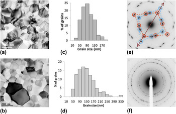
 0].Reference Niwa and Kato20 As explained in Fig. 1, these films consist of just two grain families, rotated 90° in-plane with respect to each other, with both having a (110) out-of-plane texture. More importantly, the Schmid factor of all active slip systems in every grain is identical (0.408) when the films are subjected to uniaxial tension along the [001] direction of either grain family. The nontextured films with a heterogeneous microstructure were obtained by sputter depositing aluminum on Si (001) wafers with the native silicon dioxide layer intact. The native oxide layer disrupts the epitaxial growth of aluminum, leading to films with random orientation of grains and a fairly heterogeneous microstructure (the maximum Schmid factor of grains varies from 0.27 to 0.5). The base pressure in the sputtering chamber during deposition of these films was 5 × 10⁻⁸ Torr, except for the 225 and 160 nm textured film (1.5 × 10⁻⁸ and 10−7 Torr, respectively). All the films were deposited at room temperature at a rate of 4 nm/min.
(a, b) Bright field transmission electron micrograph of 160-nm thick (110) textured film and 165-nm thick nontextured film. (c, d) Grain size distribution of the textured and nontextured film. (e) Typical diffraction pattern of the textured films. The (110) out-of-plane texture can be inferred from the characteristic arrangement of 111 (first ring), 200 (second ring) and 220 (third ring) diffraction spots. The spots encircled in red and connected by red lines are from grains loaded along [100] direction since the [200] spot is parallel to the straining direction (double arrow). The spots marked by blue circles correspond to the second set of grains that are rotated 90° in plane with respect to the first set of grains; for these grains the [022] spot is parallel to the straining direction. (f) Typical diffraction pattern of the nontextured films showing no preferred orientation of the grains.

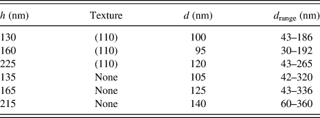
Three aluminum films with (110) texture of 130, 160, and 225 nm thickness and three nontextured films with thickness 135, 165, and 215 nm were synthesized using this method. Freestanding aluminum tensile specimens were then cofabricated with microscale tensile testing devices using the process outlined in Han and Saif.Reference Han and Saif21 The tensile testing devices have built-in gauges that allow simultaneous stress and strain measurements during deformation. Both the (110) textured and nontextured films were under compressive stress in the as-deposited state and, therefore, the freestanding specimens buckled when they were released from the substrate. Since the buckling stress is very low (<0.1 MPa), the specimens are almost macroscopically stress-free before loading.
The microstructure of the films was examined through transmission electron microscopy (TEM), which showed that the (110) textured films had slightly smaller mean grain sizes (d) compared to the nontextured films of comparable thickness (Table I). The (110) textured films also had a slightly narrower distribution of grain sizes compared to the nontextured films, which contained a few extremely large (∼3d) grains [Fig. 1(b)].
Microstructural details of the films tested in this study.

h is the thickness, and d range is range of grain sizes in each film.
B. Tensile testing procedure
The mechanical behavior of the thin film specimens was investigated through identical quasi-static tensile load–unload experiments inside an environmental scanning electron microscope. Uniaxial tensile strain was imposed in small increments/decrements on the specimens, and the deformation was then halted for a period of 1 min, after which the stress–strain data was recorded. The average strain rate over a complete load–unload cycle was ∼10−5/s. The strain rate during the strain increments/decrements was ∼10−4/s. Loading was along the [001] direction of the Al[001]//Si[110] grain family [Fig. 1(e)] for the textured films and along a random direction for the nontextured films. To eliminate variations in mechanical behavior that can arise from specimen size, the width (30 μm) and length (350 μm) of all the test specimens were kept constant. Thus, by ensuring uniformity in the fabrication process, loading rate, and specimen dimensions across all films, we were able to isolate the effect of texture on their deformation behavior. To ensure the repeatability of the observations, at least two specimens were tested from each film. The main source of error in stress measurement comes from the calibration of the force sensing beams in the tensile testing devices. Based on the calibration data, the error was less than 2% of the measured stress value (95% confidence level) for all the films. The error in strain measurement was ∼5 × 10⁻⁵ for all specimens.
III. RESULTS AND DISCUSSIONS
A. Mechanical behavior of textured and nontextured films
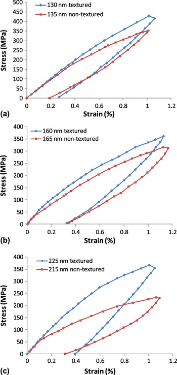
The stress–strain response of a representative specimen from each film is shown in Fig. 2. To highlight the effect of microstructural heterogeneity, the deformation response of films with similar thickness is plotted together. The textured films consistently attain higher stresses compared to nontextured films of comparable thickness, even though their grain sizes are roughly similar. Furthermore, the textured films show a well-defined elastic regime up to about 0.2–0.3% strain during loading, whereas the stress–strain curves of the nontextured films (except the 135-nm-thick film) deviate from elastic behavior even at strains below 0.1%. The behavior of the textured and nontextured films during unloading is quite dissimilar as well. The textured films show a predominantly elastic response with only a small deviation from elastic behavior toward the end of unloading. On the other hand, the nontextured films exhibit a substantial deviation from elastic behavior even at stresses as high as 150 MPa, resulting in a large early Bauschinger effect.
Stress–strain curves for the textured and nontextured films. The textured films show higher stresses and a less pronounced Bauschinger effect compared to nontextured films of comparable thickness.

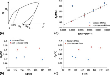
The stress–strain curves in Fig. 2 clearly illustrate the qualitative differences between the textured and nontextured films. To quantify these differences, we calculated the yield stress (σ y) and “Bauschinger strain” (ε B) in the films by adopting the conventions described in Fig. 3(a). Briefly, the yield stress of each film was obtained by averaging the stress at 0.2% offset strain during the first deformation cycle for all specimens from that film. ε B is defined as the difference between ε p, the expected plastic strain, and the actual plastic strain. As evident from Fig. 3(b), textured films show Bauschinger strains that are 30–60% lower compared to the nontextured films. This trend is not affected irrespective of whether ε B is plotted as a function of film thickness or mean grain size [Fig. 3(c)], the two parameters that are often used to interpret the plastic behavior of thin films. This strongly suggests that the difference in behavior is the result of the difference in grain orientations between the two sets of films. Note that since ε B varies with the applied plastic strain [Fig. 4(a)], ε p was kept approximately constant for all the films (0.36–0.41%).
(a) Convention used for calculating yield stress (σy) and Bauschinger effect. ε p is the plastic strain expected if there is elastic unloading. ε B, the Bauschinger strain, is the difference between ε p and the actual plastic strain. (b, c) Bauschinger strain plotted against film thickness and grain size. ε B is substantially larger for the nontextured films compared to textured films irrespective of film thickness or grain size. (d) Yield stress (obtained from multiple specimens) of textured and nontextured films as a function of 1/hd 0.5. When both the thickness and grain size effect are taken into account, yield stress is higher for the textured films compared to nontextured films. The dashed line is the linear trend line of yield stress for the nontextured films. Error bars represent the estimated error in the yield stresses.

(a) Variation of ε B with ε p in the 160-nm textured film and 165-nm nontextured film, obtained from multiple specimens. ε B remains nearly constant once ε p becomes sufficiently large. (b) Stress–strain response of a 160-nm textured film specimen subjected to different strains. The stress–strain slope reduces substantially at higher applied strains, indicating macroscopic plastic deformation, after which there is little increase in internal stresses and Bauschinger effect.

On the other hand, textured films have relatively higher yield stresses compared to the nontextured films. Several experiments have shown that the yield stress of thin films depend both on their thickness (h) and mean grain size (d). The yield stress scales as the reciprocal of the film thickness (1/h) and square root of the grain size (1/d 0.5).Reference Xiang and Vlassak22 In our experiments, there is slight variation in both the thickness and grain size among the textured and nontextured films. Therefore, to provide a fair comparison, we have plotted the yield stress of the films as a function of 1/hd 0.5 [Fig. 3(d)]. As evident from the figure, the 225-nm and 130-nm thick textured films have noticeably higher yield stress compared to the nontextured films, whereas the yield stress of the 160-nm thick textured film was quite similar.
We note that none of the films examined in our study showed noticeable grain growth during deformation, in contrast to earlier experiments.Reference Legros, Gianola and Hemker5, Reference Gianola, Van Petegem, Legros, Brandstetter, Van Swygenhoven and Hemker12 We believe the reason for this behavior is twofold. First, the strains applied in our experiments are much lower than those applied in Refs. [Reference Legros, Gianola and Hemker5,Reference Gianola, Van Petegem, Legros, Brandstetter, Van Swygenhoven and Hemker12], where grain growth was seen mainly for large strains. Second, the films in those studies were synthesized using pulsed deposition specifically to avoid the growth of columnar grains, which was not the case with our films.
B. Mechanism for early Bauschinger effect
The marked differences between the textured and nontextured films show the substantial influence of heterogeneity on the mechanical behavior. To understand how heterogeneity affects the macroscopic response, we first consider the large early Bauschinger effect in the nontextured films. Because of the random orientation of grains, it is likely that some of the grains are favorably oriented for dislocation glide, whereas others have a less favorable orientation. During loading, favorably oriented grains that are also relatively large start deforming plastically at low macroscopic strains and relax their stresses. In contrast, smaller/less favorably oriented grains deform elastically until much higher strains and consequently have higher stresses than the overall macroscopic stress. In other words, there is an extended microplastic deformation. As a result, the favorably oriented grains go into compression during unloading even when the overall stress is still tensile. This leads to reverse plasticity in these grains, resulting in Bauschinger effect.Reference Rajagopalan, Han and Saif23 In this context, it is worth noting that investigations on copper thin filmsReference Baker, Kretschmann and Arzt24 have shown that the plastic relaxation strongly depends on the orientation of the grains.
In the (110) textured films, on the other hand, the stresses in the grains are substantially more uniform due to the following reason. The textured films have only two major grain orientations, and because the tensile loading axis is aligned with the [001] direction of one set of grains and the [110] direction of the other set, all the grains have several [110]{111} slip systems with an identical Schmid factor of 0.408. In other words, all grains have equally favorable orientation for dislocation glide. Therefore, orientation-induced variations in plastic relaxation among the grains is greatly reduced. In addition, the grain size distribution is also slightly narrower, which further reduces the difference in stress levels among the grains. As a result of this more homogeneous stress distribution, Bauschinger effect is significantly reduced. Note that while the Bauschinger effect in the textured films is small relative to the nontextured films, it is still very large compared to coarse-grained metalsReference Christodoulou, Woo and Macewen25 and single crystals.Reference Pedersen, Brown and Stobbs26 This suggests that the deformation in nanocrystalline metals is intrinsically more heterogeneous than coarse-grained metals.
Next, we consider the smaller elastic regime and yield stresses of the nontextured films compared to textured films. Both these observations can also be explained by the heterogeneous microstructure of the nontextured films. As mentioned earlier, the nontextured films have several unusually large grains that are likely to have low stresses for dislocation activation. Therefore, a small strain (∼0.1%) is sufficient to initiate plasticity in these grains, which in turn leads to a macroscopic deviation from elastic behavior. But the heterogeneous microstructure also results in a more gradual transition to homogeneous plastic deformation. For example, in the 215-nm thick nontextured film [Fig. 2(c)] the first set of grains yield (as measured by a change in stress–strain slope) at around 0.1% strain. Full yielding (where stress–strain slope becomes nearly zero) occurs at about 1.05% strain. The corresponding values for the 225-nm thick textured film are approximately 0.3% strain and 1% strain. In other words, the region of microplastic deformation is smaller for the textured films compared to the nontextured films. As a result, the yield stress as determined by the stress at 0.2% offset strain is higher for the textured films. This result is consistent with computational studies,Reference Berbenni, Favier and Berveiller27 which show a reduction in yield stress with increased heterogeneity even when the mean grain size remains unchanged.
We note that while the textured films have a smaller microplastic region, they have a higher apparent work hardening rate compared to the nontextured films. Because the textured films have only two in-plane variants, only tilt grain boundaries can be present in these films. In contrast, the nontextured films will have boundaries of mixed (tilt and twist) character. This difference in grain boundary structure between the two sets of films could be one of the factors affecting their apparent work hardening rates.
In the above discussion, we argued that the Bauschinger effect is caused by internal stresses that develop as a result of microplastic deformation. If this were true, the magnitude of Bauschinger effect (ε B) should not increase once the majority of grains start deforming plastically, that is, the deformation becomes more homogeneous. To test this hypothesis, we studied the relation between ε B and ε p for the 160 nm textured film and the 165 nm nontextured film [Fig. 4(a)]. The results clearly show that ε B saturates as ε p becomes sufficiently large (∼0.8%). An examination of the stress–strain curves of a 160 nm textured film specimen [Fig. 4(b)] provides further support for this hypothesis. As the applied strain becomes larger (second deformation cycle) the stress–strain slope reduces dramatically, indicating that a majority of grains are deforming plastically. Once the deformation becomes more homogeneous, there is little change in the internal stresses and consequently ε B.
C. Interplay between microstructural size and heterogeneity
Our observations clearly delineate the importance of heterogeneity in determining the macroscopic behavior of nanocrystalline metals. In particular, they indicate that the yield strength of these materials can be altered by the heterogeneity of their microstructure. The scatter in the yield stresses of nanocrystalline metals reported in literatureReference Meyers, Mishra and Benson28 could, at least in part, be related to variations in microstructural heterogeneity. We also note that the mechanism of early Bauschinger effect in freestanding films examined here is fundamentally different from that of passivated films.Reference Xiang and Vlassak22 In passivated films, Bauschinger effect is caused by the blockage of dislocations at the film/passivation layer interface. Here, Bauschinger effect is caused by the intrinsic heterogeneity of the microstructure.
Even though there have been few systematic experimental studies of the role of microstructural heterogeneity, researchers have investigated this aspect of the deformation of nanocrystalline metals through a combination of theoretical modeling and continuum scale numerical simulations. For example, Zhu et al.Reference Zhu, Asaro, Krysl and Bailey29, Reference Zhu, Asaro, Krysl and Bailey30 developed a framework to incorporate the effect of grain size distribution, and the contributions from different deformation mechanisms, on the behavior of nanocrystalline metals. Similarly, Berbenni et al.Reference Berbenni, Favier and Berveiller27 incorporated a log-normal distribution of grain sizes into an elastic-viscoplastic model to simulate the behavior of polycrystalline aggregates. Using this model, they showed that increasing grain dispersion leads to higher internal stresses and lower yield stresses and that these effects become more pronounced at smaller grain sizes. Shishvan et al.Reference Shishvan, Nicola and Van der Giessen31 carried out 2D discrete dislocation plasticity simulations to investigate the Bauschinger effect in freestanding thin films. They showed that the dispersion of grain size in a film together with the size-dependence of yield strength leads to significant Bauschinger effect.
A few experimental studies have also pointed to the importance of microstructural heterogeneity in nanocrystalline metals. Lonardelli et al.,Reference Lonardelli, Almer, Ischia, Menapace and Molinari19 for example, have shown that significant strain recovery occurs in bulk nanocrystalline-ultrafine-grained aluminum as a consequence of microstructural heterogeneity. Similarly, the early Bauschinger effect in Cu/Nb nanocomposite wiresReference Thilly, Renault, Van Petegem, Brandstetter, Schmitt, Van Swygenhoven, Vidal and Lecouturier32 has been shown to be caused by microstructural heterogeneity, and based on this, a new criterion for yielding in nanocrystalline metals has been suggested.Reference Thilly, Van Petegem, Renault, Lecouturier, Vidal, Schmitt and Van Swygenhoven33 In a recent work, in situ TEM straining experiments with concurrent stress–strain measurements were performed to study the effect of microstructural heterogeneity in nanocrystalline metal films. It was found that a heterogeneous microstructure led to extended microplasticity and a large Bauschinger effect, whereas a homogeneous microstructure resulted in a sharper elastic–plastic transition and limited Bauschinger effect.Reference Rajagopalan, Rentenberger, Karnthaler, Dehm and Saif34
It is worth noting that while coarse-grained metals can also have heterogeneous microstructures, they show little early Bauschinger effect or strain recovery after unloading. This suggests that microstructural heterogeneity becomes increasingly important when the average grain size reduces to the nanometer scale. In other words, it is the interplay between heterogeneity and size dependence of properties like yield strength that leads to these unusual mechanical behaviors.
IV. CONCLUSIONS
In summary, we studied the mechanical behavior of nanocrystalline aluminum films with vastly different levels of microstructural heterogeneity through uniaxial tensile experiments. The films with a more homogeneous microstructure (identical Schmid factors for all grains) show higher yield stresses compared to films with a heterogeneous microstructure but exhibit significantly less Bauschinger effect, despite having similar thickness and mean grain size. Our results emphasize the importance of the interplay between microstructural size and heterogeneity in shaping the mechanical behavior of nanocrystalline materials.
ACKNOWLEDGMENTS
This material is based upon work supported by the National Science Foundation under Award No. NSF CMMI-0728189. The aluminum specimens were fabricated in Micro-NanoMechanical Systems Cleanroom and Micro Nano Technology Laboratory at the University of Illinois at Urbana-Champaign (UIUC). The experiments were performed at the Beckman Institute at UIUC. Discussions with Prof. Christian Rentenberger regarding the TEM analysis of the films are gratefully acknowledged.