I. INTRODUCTION
The ability to modulate the properties of gallium nitride (GaN) for various applications, such as optoelectronics and biosensors, is an ongoing research endeavor. Chemical functionalization extends the utility of GaN beyond traditional applications into environments, previously unexplored. This can be seen in the surface modification of GaN that permits matching of the HOMO and LUMO levels of the native band gap to that of organic dye molecules used for sensitization in dye-sensitized solar cells (DSSCs). Reference Stutzmann, Garrido, Eickhoff and Brandt1 In addition, the placement of biomolecules on the surface of GaN-based devices can result in high sensitive and selective biosensors. Reference Makowski, Kim, Gaillard, Janes, Manfra, Bryan, Sitar, Arellano, Xie, Collazo and Ivanisevic2 When compared to other III–V materials, such as InN or GaAs, GaN offers superior properties both electrical and chemical. GaN exhibits high-electron mobility, efficient recombination paths, and large breakdown voltages required for electronic devices. Reference Morkoc3 This material is also very stable under a wide range of chemical conditions and solvents. Reference Arisio, Cassou and Lieberman4 In addition, several reports have demonstrated excellent biocompatibility. Reference Hofstetter, Howgate, Schmid, Schoell, Sachsenhauser, Adiguzel, Stutzmann, Sharp and Thalhammer5,Reference Jewett, Makowski, Andrews, Manfra and Ivanisevic6
A number of research groups have described how to modify the properties of the GaN surfaces by attaching various functional molecules to the surface. Reference Huang, Chang, Chang, Lee, Chang, Kwo, Wu and Hong7 Schwarz et al. successfully attached 1-alkenes to GaN surfaces via a photochemical and thermal functionalization process. Reference Schwarz, Cimalla, Eichapfel, Himmerlich, Krischok and Ambacher8 The utilization of a controlled environment for the chemisorptions of haloanilines, Reference Bermudez9 aniline, Reference Bermudez10 pyrroline, Reference Bermudez11 water, Reference Bermudez and Long12 and fluorine Reference Bermudez13 has also been demonstrated. An evaporation technique has also been used for the adsorption of thiols on a GaN surface. Reference Bermudez14 A Grignard reaction sequence has been reported to result in the successful attachment of alkyls to a GaN surface. Reference Peczonczyk, Mukherjee, Carim and Maldonado15 Olefin metathesis has been shown to lead to the covalent attachment of peptides to the GaN (0001) surface. Reference Makowski, Zemlyanov and Ivanisevic16,Reference Makowski, Zemlyanov, Lindsey, Bernhard, Hagen, Chan, Petersohn, Medow, Wendel, Chen, Canter and Ivanisevic17 Furthermore, DNA binding olefin has been placed on the material by photochemical activation. Reference Kim, Colavita, Metz, Nichols, Sun, Uhlrich, Wang, Kuech and Hamers18 GaN nanowire surfaces have also been coated by aluminum, titanium, and silicon oxides using an atomic layer deposition technique to provide enhanced binding prior to chemical modification. Reference Guo, Abdulagatov, Rourke, Bertness, George, Lee and Tan19 Self-assembled molecules of alkylphosphonic acid are also shown to readily form monolayers on the GaN films. Reference Ito, Forman, Cao, Li, Eddy, Mastro, Holm, Henry, Hohn and Edgar20 All these reports have demonstrated the potential opportunities offered by terminating the surface of GaN with different chemistries. However, with regards to processing, there remains a significant amount of improvement before industrial application is feasible. Many of these reports rely on controlled environments, multiple steps, and the use of organic solvents, and in some instances, the need to use adsorbates that are not commercially available or offered only for certain functional groups and alkyl chain lengths. There is a need for a more sustainable green approach that uses milder processing conditions that can be adapted to several classes of adsorbates to provide reproducibility and scalability required for semiconductor processing of GaN.
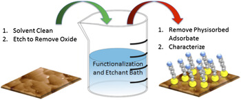
This review focuses on an in situ solution-based functionalization method for modifying the surface of GaN. This technique is advantageous due to the ability to both etch and attach groups to the surface via a single, solution-based step. As shown schematically in Fig. 1, this is a beaker-based procedure that requires no special measures and can be readily adapted to small and large samples alike. We apply this method to modify the surface properties of GaN material with different crystallographic orientations and surface qualities and review the sensitivity of the material to different chemical treatments. We further discuss the types of adsorbates compatible with the conditions utilized during in situ functionalization. A substantial portion of the review summarizes the characterization data gathered to assess changes in the topography, surface chemistry, optical, and electronic properties of GaN post functionalization. In addition, the review discusses the passivation capabilities of in situ functionalization and the role of environmental stability based on the mass spectrometry data. The review concludes with an outlook on future opportunities associated with in situ functionalization.
Pictorial representation of the in situ functionalization process.

II. IN SITU MODIFICATION OF GaN IN A BEAKER
A. Mechanism of surface attachment
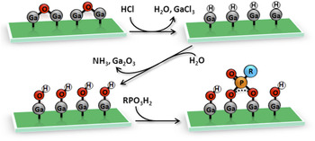
The in situ approach proceeds through a single, solution-based process to achieve surface modification, but requires several additional steps for sample preparation and characterization, Fig. 2. The process can be divided into four different steps: cleaning, etching, adsorbate binding, and supplemental surface capping. In the cleaning step, the atmospheric carbon contaminants are removed via organic solvent baths and a native oxide monolayer is spontaneously formed due to oxygen availability in the ambient environment. This is followed up with a dilute hydrochloric acid soak to remove the formed native oxide layer. The etching step involves both the formation and dissolution of various oxides on the surface, which form binding sites suitable for adsorbate attachment to the surface. During the functionalization step, the adsorbates interact with the surface and subsequently form covalent bonds with either oxides or terminal atoms on the semiconductor surface itself. The use of an acid during the in situ protocol protonates the surface and results in the formation of reactive hydrogen species that provide reaction centers in subsequent etching and functionalization steps. Reference Lueangchaichaweng, Brooks, Fiorilli, Gobechiya, Lin, Li, Parres-Esclapez, Javon, Bals, Van Tendeloo, Martens, Kirschhock, Jacobs and Pescarmona21 The supplementary capping step permits any unreacted binding sites to transform into either oxides or oxyhydroxides and thus, preventing any additional molecular binding to the surface. As a result, any remaining adsorbates in the solution are simply eluded during the washing performed at the end of the procedure.
Surface reactions associated with each step of the in situ functionalization.

Following cleaning, the GaN surface contains hydrogenated gallium sites that are exposed to wet etchant. The Ga-face of GaN material boasts a natural chemical stability that requires extreme pH environments to induce etching. Chemicals aggressive enough to etch GaN include molten NaOH, KOH, phosphoric acid, sulfuric acid, nitric acid, and oxalic acid. In an acidic environment, the etching process includes the formation of gallium oxide (Ga2O3) and ammonia from GaN in the presence of water. The water promotes the mechanism of etching, while the acids or bases act as catalysts. The presence of Ga2O3, a soluble species at pH less than 3.0, enables the mechanism of dissolution of gallium into solution. The chemical reaction describing the etching process is shown by Reference Jung, Ahn, Baik, Kim, Pearton, Ren and Kim22 :
 $$2{\rm{GaN}}\left( {\rm{s}} \right) + 3{{\rm{H}}_2}{\rm{O}}\left( {\rm{l}} \right) \to {\rm{G}}{{\rm{a}}_2}{{\rm{O}}_3}\left( {\rm{s}} \right) + 2{\rm{N}}{{\rm{H}}_3}\left( {{\rm{aq}}{\rm{.}}} \right)\quad .$$
The etching process enables oxide formation as well as dissolution of oxides. Based on the nature of the adsorbate being used, the presence of the oxide can be beneficial for additional adhesion or subsequent surface attachment, or it can be problematic. For example, attaching thiol groups to the GaN surface requires the removal of oxides to ensure binding of the sulfur group to available Ga sites. The thiols bind to low valence metal atoms, and the presence of oxygen causes repulsion due to charge similarities. Reference Sheen, Shi, Maartensson, Parikh and Allara23,Reference Bain24 In contrast, for phosphonic acid linkages, the removal of the native oxide layer is not required. The phosphonic groups bind with the surface oxygen atoms through the three groups present on these molecules. Reference Paniagua, Hotchkiss, Jones, Marder, Mudalige, Marrikar, Pemberton and Armstrong25 These groups do not require the use of extremely pure environment during the functionalization process.
The supplementary capping step involves the reaction on the remaining available sites on the GaN surface after adsorbate binding. In this way, a secondary species can adhere to available sites to promote bifunctionalized surface properties. Until now, only capping with hydrogen peroxide forming hydroxyl or oxyhydroxyl species has been attempted. The presence of water and peroxide species in the solution facilitates oxide species differentiation as a way to identify aqueous environmental stability. An advantage of in situ functionalization is the ability to perform all of these steps in one beaker process for a short period of time at slightly elevated temperatures. The increase of process temperature accelerates the etching process but may result in poor surface quality and excessive pit formation. The use of only slightly elevated temperatures and solution-based methods ensures a safer, environmentally cleaner approach to modulate the properties of GaN by attaching organic molecules to its surface.
B. Dependence on GaN surface polarity and quality
GaN crystals have wurtzite crystal structure, belong to the P63
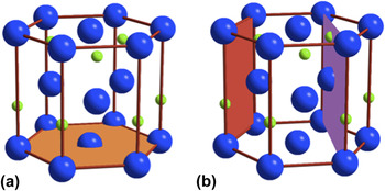
mc crystallographic group and are noncentrosymmetric, lacking inversion symmetry. The wurtzite close-packed structure is formed by alternate planes, of either Ga or N atoms, stacking along the hexagonal [0001] direction, often defined as c-axis. The bonds, forming alternatively single bond parallel to the c-axis and triple bonds symmetrically surrounding the c-axis are responsible for forming two subsequent interplanar distances of different length. As a result, the crystal exhibits polarity in the c-direction. For the GaN crystals, it is correlated with the chemical nature of the topmost surface: the (0001), c, and (
 $000\bar 1$
), −c, surface planes are defined as crystal surface terminated either by Ga or N atoms, respectively [Fig. 3(a)]. Furthermore, the polarity of the wurtzite nitride materials leads to piezoelectric and spontaneous polarization fields along the [0001] direction, which is well known to have a detrimental effect on optoelectronic devices due to charge separation and quantum-Stark effect,
Reference Nakamura26
and a beneficial effect on doping flexibility of two-dimensional electron gas in field-effect transistors although it predetermines their normally-on regime. Aiming to circumvent the polarity effect of the wurtzite GaN, using the so-called nonpolar planes for growth on and device active region aligned to, has been suggested. Both the
 $\left( {11\bar 20} \right)$
, a-, and
 $\left( {1\bar 100} \right)$
, m-, surface planes are perpendicular to the basal c-plane of the wurtzite crystal structure [Fig. 3(b)] and are characterized by equal numbers of Ga and N atoms and no polarity effect.
Schematic representation of (a) polar c-plane GaN and (b) nonpolar a-plane (purple) and m-plane (red) GaN surface polarities.

The growth along the [0001] polar direction was preferred and better controlled for long time, but recently different approaches have been proposed to accomplish growth along different crystallographic directions and polarity by hydride vapor phase epitaxy, Reference Amano, Nishinaga and Kuech27 metalorganic chemical vapor deposition, Reference Bickermann, Paskova, Nishinaga and Rudolph28 or molecular beam epitaxy. Reference Koblmuller, Lang, Young, Speck, Nishinaga and Kuech29 The GaN surfaces with different crystallographic orientations and polarities have different chemical stabilities due to their different bond arrangements, which requires different material processing. Reference Hite, Garces, Goswami, Mastro, Kub and Eddy30 In addition, it was also found that the different surface energies allow for different growth rates and impurity incorporation efficiencies. Reference Cruz, Keller, Mates, Mishra and DenBaars31,Reference Browne, Young, Lang, Hurni and Speck32 These findings provoked further scientific interest in studying the effect of crystal orientation and polarity on the available binding sites and response to functional molecules on the surface. In situ functionalization of polar and nonpolar GaN with phosphonic acid derivatives was recently performed by our group. Reference Wilkins, Greenough, Arellano, Paskova and Ivanisevic33
Currently, there are two main approaches for producing GaN, namely heteroepitaxial growth on widely available foreign substrates and homoepitaxial growth using bulk GaN substrates of still limited size and relatively expensive. The former is characterized by high dislocation density (typically in the range of 109–1010 cm−2), whereas the latter possesses several orders of magnitude lower dislocation density. This consequently determines different surface characteristics of the two types of material due to the surface depressions in the vicinity of the dislocations intersecting the surfaces. The different surface quality is expected to have different sensitivity toward the chemical treatments, and was another main focus of our studies.
C. Adsorbate choices
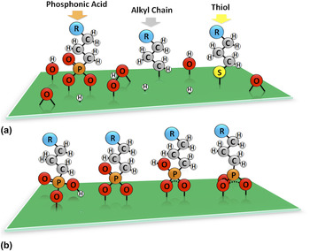
Many different adsorbates have been used as passivating agents on semiconductor surfaces. Of these, several commercial reagents offer convenient, reliable, and affordable choices for in situ functionalization. In particular, our initial work was focused on exploring GaN treatments with thiol terminated and phosphonic acid derivatives, Fig. 4(a). The attachment of sulfur groups to III–V semiconducting materials has been intensively explored for GaAs. Reference Sandroff, Nottenburg, Bischoff and Bhat34,Reference Lunt, Santangelo and Lewis35 Research into the functionalization of GaAs surfaces with long-chained thiols Reference Sheen, Shi, Maartensson, Parikh and Allara23 such as octadecylthiol Reference Bain24,Reference Adlkofer and Tanaka36 has provided insight into the binding mechanism of thiol groups to III–IV semiconductor surfaces. The binding mechanism of thiol groups involves the attachment of the sulfur species to the exposed metal atom. This requires oxide removal prior to attachment. Among the thiols, there are very few commercially available water-soluble options. Thioglycolic acid and cysteamine are two readily available water-soluble thiols. It has been demonstrated that cysteamine has the ability to limit the formation of oxides on GaAs and InAs bulk materials Reference Ding, Moumanis, Dubowski, Tay and Rowell37–Reference Stine and Petrovykh39 in addition to providing reduced toxicity in biological environments. Reference Lovrić, Bazzi, Cuie, Fortin, Winnik and Maysinger40 The in situ functionalization of thiols on GaN affords a mechanism for forming and removing gallium oxide to provide binding sites for thiol anchoring. In this way, a completely pristine surface is not a requirement. Reference Wilkins, Paskova and Ivanisevic41
(a) Difference in surface attachment modes based on adsorbate mode; (b) the possible binding modes of phosphonic acid groups to the surface.

Another potential adsorbate for GaN surface modification is phosphonic acid, a derivative of phosphoric acid, that can bind either directly onto low valence metal atoms or pre-existing oxide layers. Reference Paramonov, Paniagua, Hotchkiss, Jones, Armstrong, Marder and Bredas42 Specific reaction conditions such as solvent, time, and temperature can be varied to graft organophosphoric acid with the aid of Ga2O3 prior to its complete dissolution from the surface. Phosphonic acid and its derivatives have been used to passivate the surface of GaN in previous work. Reference Ito, Forman, Cao, Li, Eddy, Mastro, Holm, Henry, Hohn and Edgar20 The advantage of using these adsorbates for attachment is the ability to customize the side and end groups along the carbon backbone of the phosphonic acid chain. The presence of certain groups provides the capability of altering numerous surface properties. Reference Paniagua, Hotchkiss, Jones, Marder, Mudalige, Marrikar, Pemberton and Armstrong25,Reference Chen, Ruther, Tan, Bishop and Hamers43,Reference Hotchkiss, Li, Paramonov, Paniagua, Jones, Armstrong, Bredas and Marder44 In the case of DSSCs, the use of phosphonic acids limits the amount of surface charge recombination and promotes work function matching. Reference Sharma, Kippelen, Hotchkiss and Marder45 The various proposed modes of phosphonic group attachment to the surface of GaN are shown in Fig. 4(b). The presence of the two hydroxyl groups and a double-bonded oxygen on the phosphonic acid head group provides three possible binding points. Phosphonic acids can be present in various binding conformations including monodentate, bidentate, and tridentate. Reference Brennan, Portoles, Liddell, Moore, Moore and Gust46 Various groups studying the attachment of phosphonic acid derivatives on the GaN surfaces using organic solvents such as tetrahydrofuran (THF) and toluene at elevated temperatures determined that phosphonic acid derivatives bind to oxide surfaces predominately through a bidentate mode. Reference Paniagua, Hotchkiss, Jones, Marder, Mudalige, Marrikar, Pemberton and Armstrong25,Reference Paramonov, Paniagua, Hotchkiss, Jones, Armstrong, Marder and Bredas42 Until now, in situ functionalization with phosphonic acid derivatives on the GaN surfaces has been performed with both short- and long-chained molecules. Reference Wilkins, Greenough, Arellano, Paskova and Ivanisevic33,Reference Wilkins, Paskova and Ivanisevic47 In addition, in situ functionalization with short phosphonic acid derivatives such as ethephon can result in a well-passivated GaN surface that can be further tailored with biomolecules such as peptides and used in harsh conditions such as exposure to ionizing radiation. Reference Berg, Nolan, Paskova and Ivanisevic48
III. PROPERTY CHANGES AFTER IN SITU SURFACE MODIFICATION
A. Topographical changes
Morphological characteristics of passivated surfaces can be determined with water goniometry (water contact angle) and atomic force microscopy (AFM). Water contact angle allows determination of surface hydrophobicity through the degree of surface coverage and adsorbate chemistry. This is controlled via the coverage of functional groups on the surface, topography of the sample, and any contamination on the surface. Reference Hotchkiss, Malicki, Giordano, Armstrong and Marder49,Reference Wilkins, Paskova and Ivanisevic50 For thiol functionalization, the water contact angle response varied more by the different etchant temperatures used rather than the presence or lack thereof of cysteamine. Reference Wilkins, Paskova and Ivanisevic41 The decrease in water contact angle is more sensitive to the surface topography (the quantity and size of surface defects), which was seen at higher temperatures. Although cysteamine presence on the surface was identified, the surface coverage was not uniform. Short-chained adsorbates are known to result in incomplete coverage and often require secondary annealing and/or lengthy deposition techniques. Reference Hotchkiss, Malicki, Giordano, Armstrong and Marder49,Reference Cho, Chu, Chen, Huang and Tao51 This could be controlled not only by the concentration used, but also the solvent present during deposition. Until now, this is the first reported instance of functionalization of GaN with an aqueous thiol solution. With respect to crystallographic orientation, the water hydrophobicity of nonpolar GaN followed a similar trend to that of polar GaN. Reference Richards, Zemlyanov and Ivanisevic52–Reference Su, Liu, Kong, Song, Li, Jin and Cheng54 By moving to short-chained phosphonic acids, the water contact angles better matched the pristine samples but still demonstrated similar nonuniform coverage. Longer chained phosphonic acids demonstrated better surface coverage in addition to slight differences due to the terminal and side groups. Reference Wilkins, Paskova and Ivanisevic47
Surface morphology alteration of bulk (low-defect-density) GaN and of thin layer (high-defect-density) GaN upon various adsorbates and variable etchant temperature was studied by AFM. Reference Wilkins, Paskova and Ivanisevic41 The surface topography and water contact angle are closely linked, hence the increase in surface roughness (as determined by root mean square, RMS, parameter) resulted in lower water contact angle due to more potential sites to hydrate. Thin-layered GaN, having a greater degree of surface defects demonstrated higher sensitivity to etching, especially at higher temperatures. The addition of cysteamine, which limited the formation of soluble gallium oxide in phosphoric acid, limited surface roughening. This was observed for polar GaN, but less so for nonpolar GaN due to the defect-rich surface as well as increased V-species surface content. Reference Wilkins, Paskova and Ivanisevic50 For short-chained phosphonic acids, alterations to surface roughness were difficult to distinguish from large amounts of surface contamination. Reference Wilkins, Greenough, Arellano, Paskova and Ivanisevic33,Reference Wilkins, Paskova and Ivanisevic47 When utilizing long-chained phosphonic acids, surface roughness increased, particularly for 1,8-octanediphosphonic acid (ODPA), which provided statistically significant amounts of surface roughening. Of the long-chained phosphonic acids, ODPA tended to agglomerate as a result of complex binding mechanisms from a diphosphonic terminating structure.
B. Surface chemistry changes
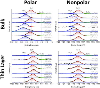
Changes in surface chemistry upon the various treatments are best investigated utilizing high-resolution x-ray photoelectron spectroscopy (XPS). Data collected via XPS can qualitatively and quantitatively identify changes after in situ functionalization. High-resolution Ga 2p 3/2 regional scans provide insight into gallium oxide formation that subsequently modulates optical properties and environmental stability. Gallium provides two primary peaks such as Ga 2p 3/2 and Ga 3d in the XPS spectra. Ga 2p 3/2 provides more surface selectivity than Ga 3d as a result of shorter penetration depth, which can provide information on depth profiling. The interaction volume can be modified via angle-resolved XPS, which utilizes either or both spectra at various photoemission angles to identify intermediate (less than 2.2 nm for Ga 3d) and shallow (less than 0.7 nm for Ga 2p 3/2) depths. The higher binding energies within this spectrum are associated with the formation of gallium oxide species. Previous work with cysteamine demonstrated the retardation of oxide production at both high and low temperatures for materials free of high quantities of defects. In a similar way, the use of short-chained phosphonic acids, particularly for 3-bromopropyl phosphonic acid, replicates the behavior, Fig. 5. Qualitatively, this does not appear to make sense due to the required oxide formation for binding of phosphonic acids on the surface. However, as will be discussed later, when compared to additional species, atomic quantities identify binding mechanisms and the degree of coverage similar to that identified by water goniometry. The qualitative analysis provides an efficient way of comparing the effect of various treatments on GaN. Reference Wilkins, Paskova and Ivanisevic41,Reference Wilkins, Paskova and Ivanisevic50 It has been identified that the lower oxide content with functionalization is associated with poorer binding and lower surface coverage. This was also observed with the long-chained phosphonic acids, and particularly for 1H,1H,2H,2H-perfluorooctane phosphonic acid (PFOPA), and 11-mercaptoundecylphosphonic acid (MUDPA). In all cases, etchant only solutions provide increased oxide content over freshly cleaned samples. In addition, more oxide was seen on the GaN polar substrates as compared to that on nonpolar ones, most likely due to increased nitrogen content promoting increased material dissolution.
Ga 2p 3/2 results highlighting surface changes due to different treatments of the samples with different polarities and crystalline qualities. Treatments were broken up into two temperature schemes (40 and 100 °C) with three different solutions (phosphoric acid, phosphoric acid with 3-bromopropyl phosphonic acid, and phosphoric acid with propylphosphonic acid). Reprinted with permission from Wilkins et al. Reference Wilkins, Greenough, Arellano, Paskova and Ivanisevic33

Quantitative analysis of XPS data offers a method of investigating the ratios of surface species present to compare coverages and degree of binding. This is performed via peak deconvolution based upon species of interest. Traditionally, Ga 3d is used as the gallium species for comparison to other atomic species due to its similar binding energies to elements such as oxygen, nitrogen, and carbon. From the atomic ratios, it was found that the addition of cysteamine to polar bulk and thin layer samples resulted in an increase in the nitrogen content on the surface. Reference Wilkins, Paskova and Ivanisevic41 The bulk nonpolar samples showed an increase in environmental carbon contamination when any of the etching processes were performed. Reference Wilkins, Paskova and Ivanisevic50 The nonpolar samples provided insight into the oxide sensitivity of the bulk and thin layer samples, as mentioned previously. The introduction of etchants to the treatment of the bulk sample showed a higher sensitivity to the oxide formation than that of the thin layer sample. In the nonpolar samples, the etching process reduced the presence of nitrogen and gallium on the surface due to surface oxide formation and environmental contamination. Treatment with phosphonic acids resulted in a similar effect. In addition to identifying contamination and oxide formation, individual species along the adsorbate carbon chain can be identified. For this reason, elements with unique XPS signatures were selected (bromine, fluorine, and sulfur). This not only provided confirmation of the surface adhesion, but also a means of identifying stability in aqueous environments. The cysteamine functionalization resulted in low nitrogen content and negligible signal from sulfur. The deconvolution of sulfur related peak (S 2p) is complicated due to the overlap with the Ga 3s peak. The peak analysis of the bromine from 3-bromopropyl phosphonic acid not only confirmed the adhesion, but also revealed a poor surface coverage via a Ga/P ratio of ∼22. The long-chained phosphonic acids not only showed better surface coverage (Ga/P ratio of 7 and 4 for MUDPA and PFOPA, respectively), but also enhanced binding characteristics exhibited by phosphonic acids versus thiols via a combined etching and functionalization process. Reference Wilkins, Paskova and Ivanisevic47 Later studies, investigating surface stability, identified the role of hydrogen peroxide dissociation on the binding, as well as the role of suboxide formation on the environmental stability.
The XPS technique has also been used to provide evidence for the successful attachment of a peptide to the GaN surface after in situ functionalization with ethephon. Reference Berg, Nolan, Paskova and Ivanisevic48 Quantitatively, an increase in the carbon content of the peptide terminated samples when compared to the clean or just etched surfaces is the evidence of successful modification of the surface. A high-resolution regional scan of the N 1s spectra of each of the samples was used to qualitatively confirm peptide attachment to the surface. A peak presence only in the samples treated with peptides near 400 eV binding energy was attributed to the binding between the peptide and the GaN surface. This peak was assigned to C–N bonds, which are prevalent in peptide species.
C. Optical properties
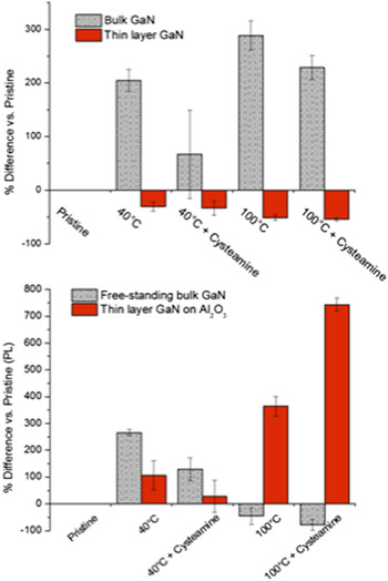
The ability to tailor optical properties of wide band gap semiconductors is an attractive benefit of the in situ functionalization. Photoluminescence (PL) is a widely used nondestructive technique for studying the optical properties via recording PL spectra of the radiative recombination of excited carriers within semiconductor materials. The effect of etching and subsequent oxide formation on the optical properties of modified surfaces was investigated by comparative PL analysis. For all GaN samples studied, the optical response was sensitive to the addition of cysteamine, Fig. 6. Reference Wilkins, Paskova and Ivanisevic41,Reference Wilkins, Paskova and Ivanisevic50 The critical angle for photon extraction varies based upon the surface topography. For ultra-flat GaN, the critical angle for photons is only 4°. GaN without polishing possesses a critical angle of 23.6°, whereas roughened GaN can have as high as three times of that. For device performance, specifically for light emitting diodes, a greater critical angle is desired. As the surface topography is controlled via etching, controlling the surface oxide formation and subsequent dissolution (as seen with the addition of cysteamine) modulates the final PL. For almost all samples, the addition of cysteamine resulted in decreased PL intensity relative to that of the samples treated with additive free etchants. Only in the case of thin-layer nonpolar GaN on sapphire, the PL intensity showed a reverse trend. This was explained by the defect contribution to the preferential sites where etching can occur and by having a defect-rich surface, the large number of etching sites begins to roughen the surface to the point where the critical angle can actually decrease.
Bar graph showing the PL changes of polar GaN (top) and nonpolar GaN (bottom) samples grown into thin and bulk layers after treatments with two temperature schemes (40 and 100 °C) and two solutions (phosphoric acid and phosphoric acid with added cysteamine). Reprinted with permission from Wilkins et al. Reference Wilkins, Paskova and Ivanisevic41,Reference Wilkins, Paskova and Ivanisevic50

After performing an in situ functionalization with short-chained phosphonic acids, the PL was used to reveal the changes due to different adsorbates and reaction conditions. Reference Wilkins, Greenough, Arellano, Paskova and Ivanisevic33 The presence of compressive strain in the thin layer GaN, as a result from lattice and thermal expansion coefficient mismatch between the GaN and the c-plane was evident by the blue-shift of the near-band gap emission peak present in the thin layer polar PL spectrum as compared to the peak position in the PL spectrum from bulk GaN sample. Reference Paskova, Hanser, Preble, Evans, Kroger, Tuomisto, Kersting, Alcorn, Ashley, Pagel, Valcheva, Paskov and Monemar55 The PL spectra showed the most intense peak present for the thin layer samples for the low-temperature sample functionalized with (3-bromopropyl) phosphonic acid. The bulk sample showed the highest intensity peak in the PL spectra of both the (3-bromopropyl) and propyl phosphonic acid functionalized samples. However, the enhancement of the emission was minimal when compared to the clean sample. The PL changes of bulk nonpolar and thin-layer nonpolar samples after various etching treatments were investigated as well. The bulk nonpolar sample showed the most intensity enhancement in the PL spectrum after higher temperature functionalization with just phosphoric acid. The presence of various phosphonic functional groups led to a minimal enhancement and, in some cases, to a decrease in the PL intensity. The nonpolar thin-layer sample showed little differences in the PL spectra for various treatments, although enhancement was observed for the lower temperature treatment of the sample with just phosphoric acid.
The effect of the attachment of long-chained phosphonic acids to polar bulk free-standing GaN on the PL spectra of the samples has also been reported. Reference Wilkins, Paskova and Ivanisevic47 The presence of phosphonic acids on the surface of the bulk GaN showed a decrease in overall intensity in the peak present in the PL spectra. This was not entirely unusual as seen for thin-layer nonpolar GaN, Fig. 6, defect-rich substrates suffer PL quenching from increased nonradiative recombination centers. The presence of PFOPA during the etching step provided an increase in the PL intensity as compared to the sample etched with just phosphoric acid. The results from this study provide evidence that the incorporation of organic phosphonic acid groups on the surface of a polar GaN sample produces significant changes in the optical properties of the material.
D. Electronic properties
The electronic properties of interfaces can be studied by investigating the charge distribution across a surface and subsequently mapping the degree of homogeneity. The use of Kelvin force probe microscopy (KFPM), a technique similar to AFM, provides information for identifying differences, both qualitatively as well as quantitatively, between the surface potential of various adsorbates. Previously reported findings of the attachment of phosphonic acids to indium tin oxide Reference Paniagua, Hotchkiss, Jones, Marder, Mudalige, Marrikar, Pemberton and Armstrong25,Reference Sharma, Kippelen, Hotchkiss and Marder45 and zinc oxide Reference Chen, Ruther, Tan, Bishop and Hamers43 show a change in the charge distribution on the surfaces based on a modulation of the work functions of the surfaces. For electronic devices, this information is crucial in determining multi-material compatibility for electrical interface interactions.
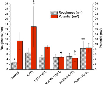
KFPM data of polar GaN samples functionalized with phosphonic acids with various terminal groups, Fig. 7, showed variations in surface charge distributions similar to that of trials on other material systems. Reference Hotchkiss, Jones, Paniagua, Sharma, Kippelen, Armstrong and Marder56 Etching with a phosphoric acid rich solution produced increased Ga2O3, which has a larger band gap than GaN by 1.4 eV that subsequently increased the surface potential. By utilizing phosphonic acids with electronegative terminal groups, the surface potential was decreased, particularly for solutions containing MUDPA and PFOPA. This provides a valuable insight on the mechanism of interfacing of inorganic semiconducting substrates with organic adsorbates. The treatment of the polar GaN with ODPA was different when compared to the MUDPA and PFOPA treatments, which is attributed to the nature of binding between this phosphonic acid and the surface (i.e., ODPA having different conformations due to complex binding mechanisms).
Bar graph comparing AFM surface roughness (nm) and KFPM surface potential (mV) of bulk Ga-polar GaN samples after treatments with 40 °C solutions of various phosphoric acid combinations (pure, diluted, and additive assisted). Reprinted with permission from Wilkins et al. Reference Wilkins, Paskova and Ivanisevic47

E. Stability
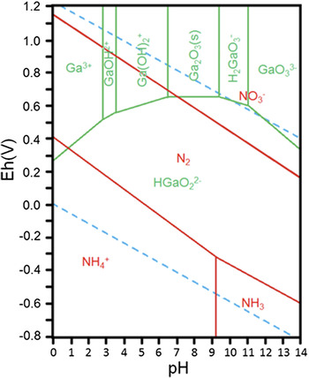
The stability of semiconductor surfaces is crucial when used for devices operating in external environments that expose the material to a myriad of conditions. For DSSCs and biosensors, the soaking of the entire structure in an aqueous environment proves inhospitable to materials with natural surface chemical instabilities or high toxicity. For III–V materials, complexities arise from the natural bispecies formation. Unlike silicon, which forms a uniform oxide of consistent electrical properties, III–V semiconductors produce oxides of various stabilities, thicknesses, and electrical properties based upon the variability in III and V oxides. GaN, having demonstrated biocompatibility, is a prime candidate for bioapplications. It boasts chemical stability as previously mentioned as well as utilizing V-species common within the body (as nitrogen makes up 3.0% of the body). Reference Frausto da Silva and Williams57 This increased chemical stability is due to a pronounced ionic bonding that results in large dissociation energies relative to other III–V materials. Reference Zaouk, Salvetat, Sakaya, Maury and Constant58,Reference Company and Haynes59 Despite nitrogen's benign nature, gallium leaching is a potential concern since it can cause chronic health effects. Reference Hart and Adamson60 Additionally, as the V-species preferentially leaches relative to the III-species, it is crucially important to cap the surface as early as possible to prevent subsequent instability. To drive this point, the degree of soluble species of both gallium and nitrogen can be seen in the Pourbaix species diagram, Fig. 8. The solubility of Ga2O3 is negligible for pH values varied between 3 and 11; however, gallium nitrates and suboxides remain relatively soluble. In this way, the surface functionalization appears to provide a protection mechanism that is not available with a native oxide layer.
Pourbaix diagram of soluble gallium and nitrogen species compiled from elemental databases. Reference Takeno62

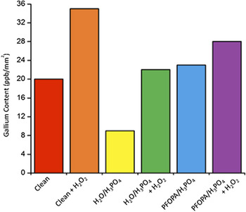
Previously published works have demonstrated decreased stability of V-groups relative to III-groups. Reference Zaouk, Salvetat, Sakaya, Maury and Constant58,Reference Foster, Collazo, Sitar and Ivanisevic61 By focusing on stabilizing gallium, a better protection can be offered. The initial studies of surface stability via functionalization used bromine terminated short-chained phosphonic acid. Reference Wilkins, Greenough, Arellano, Paskova and Ivanisevic33 Compared to an oxide terminated surface, the 3-bromopropylphosphonic acid reduced the amount of gallium species leached into solution over the course of 7 days by a whole order of magnitude. The total concentration of soluble gallium species was recorded by inductively coupled-mass spectrometry (ICP-MS). Only by adding hydrogen peroxide (H2O2) did the phosphoric acid treatment show an increased stability as a result of thicker Ga2O3 on the GaN and H2O2 interactions with the phosphonic acid.
Similar effect was seen for long-chained PFOPA as shown in the ICP-MS data, Fig. 9. Provided that the oxide is not exposed to pH extreme environments, the Ga2O3 formed via etching provides a stable protective layer. By utilizing the supplementary capping of H2O2 as previously mentioned, Fig. 2, the stability of gallium suboxides was revealed. In this way, the stabilities of gallium suboxides appear to be inferior to Ga2O3 under pH neutral conditions. Although the PFOPA treatment was demonstrated lead to stronger leaching at the tested pH, it is expected that it would have provided protection of the underlying Ga2O3 within extreme pH values as previously seen with 3-bromopropylphosphonic acid capped GaN under acidic conditions.
ICP-MS data indicating the amount of gallium leached from different GaN samples after soaking in DI water solutions for 7 days. Surface treatments follow the scheme from Fig. 2 with an additional H2O2 capping step post functionalization.

IV. CONCLUSIONS AND OUTLOOK
The surface functionalization of wide band gap III–V semiconductors provides a mechanism of modulating properties such as optical and electronic, by attaching molecules to the surface. The unique properties of GaN provide additional applications unattainable by other III–V semiconductors. These benefits, paired with the aforementioned etching and functionalization capabilities, provide a means for a relatively easy, safe, and environmentally benign methodology that has until recently remained unexplored. This review summarized results using short water-soluble thiols as well as phosphonic acid derivatives for surface functionalization of the GaN surfaces. The in situ functionalization offers a route to tune chemical, optical, and stability properties of GaN with different polarities and crystal qualities. The use of additional microscopy and spectroscopy characterization tools can offer insight into ways to increase surface coverage and stability. Furthermore, future in situ functionalization approaches need to explore additional functional groups for attachment to the GaN surface for tailored applications. Our lab is currently investigating bigger adsorbates such as porphyrins as well as carboxylic acid containing molecules.