Introduction
Size-reduced substrate integrated waveguide (SIW) has been widely researched to achieve compact bandpass filters (BPFs), because the conventional SIW has a larger volume when compared with the microstrip circuit, especially the operating frequency below 5 GHz [Reference Chen and Wu1–Reference Liu, Xiao and Zhu3]. One popular way to reduce the size of SIW is based on the equivalent magnetic boundary conditions; the half-mode SIW (HMSIW), quarter-mode SIW (QMSIW), eighth-mode SIW (EMSIW), and even the non-complete-mode SIW with general characteristic are proposed and employed to design filters with compact size [Reference Moscato, Tomassoni, Bozzi and Perregrini4–Reference Liu, Zhou, Wang and Zhang9]. Another way is based on the capacitive-loaded structure; ridge SIW (RSIW), ridged half-mode SIW (RHMSIW), and ridged half-mode folded SIW are proposed and used to design compact filters [Reference Bozzi, Winkler and Wu10–Reference Hao, Hong, Chen, Chen, Wu and Cui14].
Based on the concept of T-shaped RSIW, a pedestal SIW resonator, i.e., capacitive-loaded SIW (CLSIW) cavity, is proposed and exploited to realize size-reduced filters [Reference Nassar and Meyer15]. In [Reference Ho, Li and Chen16], a similar method is also used to realize the miniaturized SIW cavity (i.e., CLSIW cavity) to design filters with compact size and wide stopband performance. They have a characteristic of using the capacitive-loaded metal patches. However, the sizes of them are not small enough.
In this paper, a new capacitive-loaded eighth-mode substrate integrated waveguide (CLEMSIW) cavity with the ultra-compact size is proposed and analyzed in detail. Compared with the conventional SIW or EMSIW cavity counterpart, the size of the CLEMSIW cavity can be reduced by 99.32 or 97.29%. The concept of the new CLSIW cavity can be considered by combining the equivalent magnetic boundary conditions and the pedestal SIW cavity with loaded metal patch. Thus, capacitive-loaded HMSIW (CLHMSIW) and capacitive-loaded QMSIW (CLQMSIW) cavities can also be achieved and employed to design compact filters; but the sizes of CLQMSIW and CLHMSIW cavities are larger than that of CLEMSIW cavity.
To demonstrate the application of the proposed CLEMSIW cavity, a fourth-order quadruplet BPF is proposed. The negative cross-coupling is realized by an interdigital-like structure between the first and fourth cavities. Two controllable finite-transmission zeros (FTZs) can be produced to achieve sharp skirts and good out-of-band rejections. Moreover, the existence of parasitic dispersive source–load (S–L) coupling may realize three additional FTZs. In the end, a prototype filter with the center frequency (f 0) of 1 GHz and fractional bandwidth (FBW) of 10% was designed, fabricated, measured to verify the proposed structure.
The proposed CLEMSIW cavity
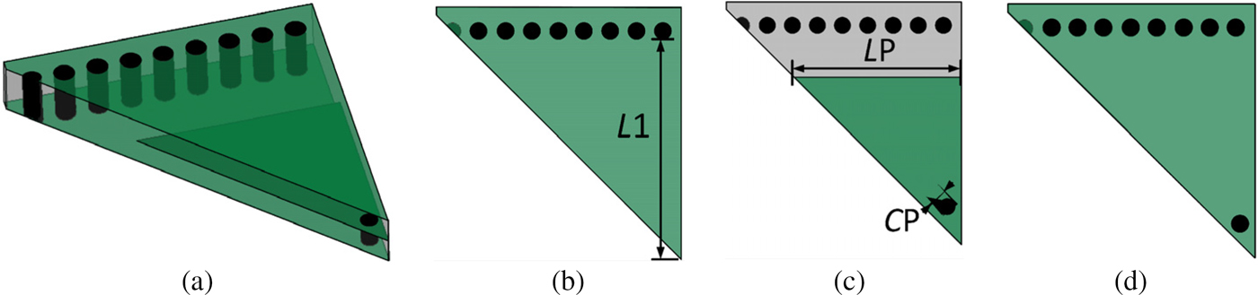
The proposed CLEMSIW cavity is derived from the conventional EMSIW cavity by adding a capacitive-loaded metal patch. The 3D view of the proposed CLEMSIW cavity is shown in Fig. 1(a), and it is composed of two substrate layers and three metal layers. The thicknesses of lower and upper substrate layers are H P and H S, respectively. All the metal layers have a thickness of 17 µm. The substrate has the dielectric constant ε r of 2.2 and a loss tangent of 0.0009. The layouts of the top, middle, and bottom metal layers are shown in Figs 1(b)–1(c), respectively. A metal via with the diameter of C P, in the lower substrate, is employed to connect the middle and bottom metal layers.
The layout of the proposed CLEMSIW cavity, (a) 3D view of the proposed CLEMSIW cavity, (b) top metal layer, (c) middle metal layer, and (d) bottom metal layer (black circle: metal hole).
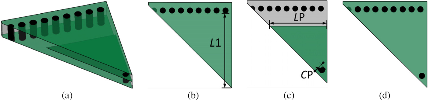
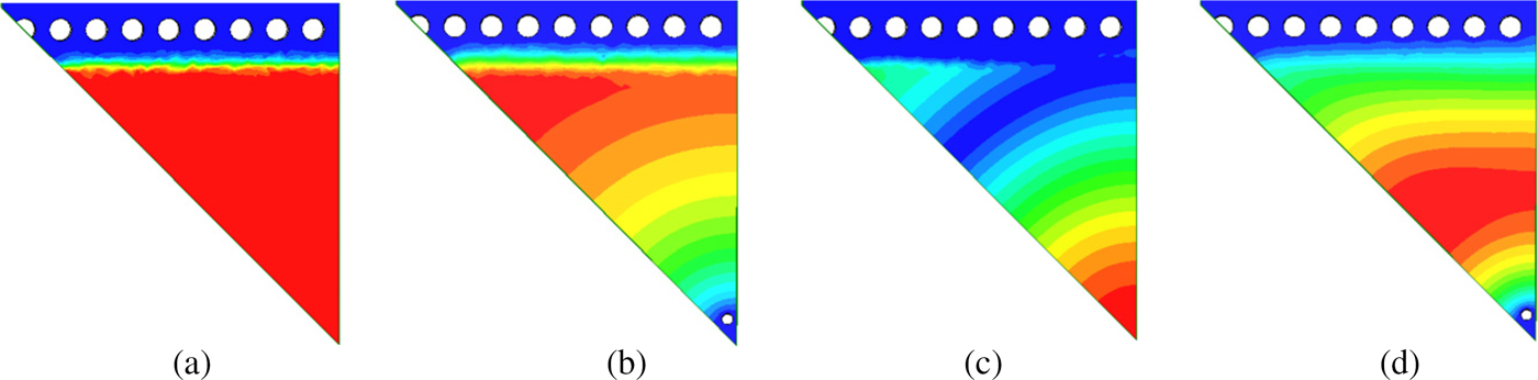
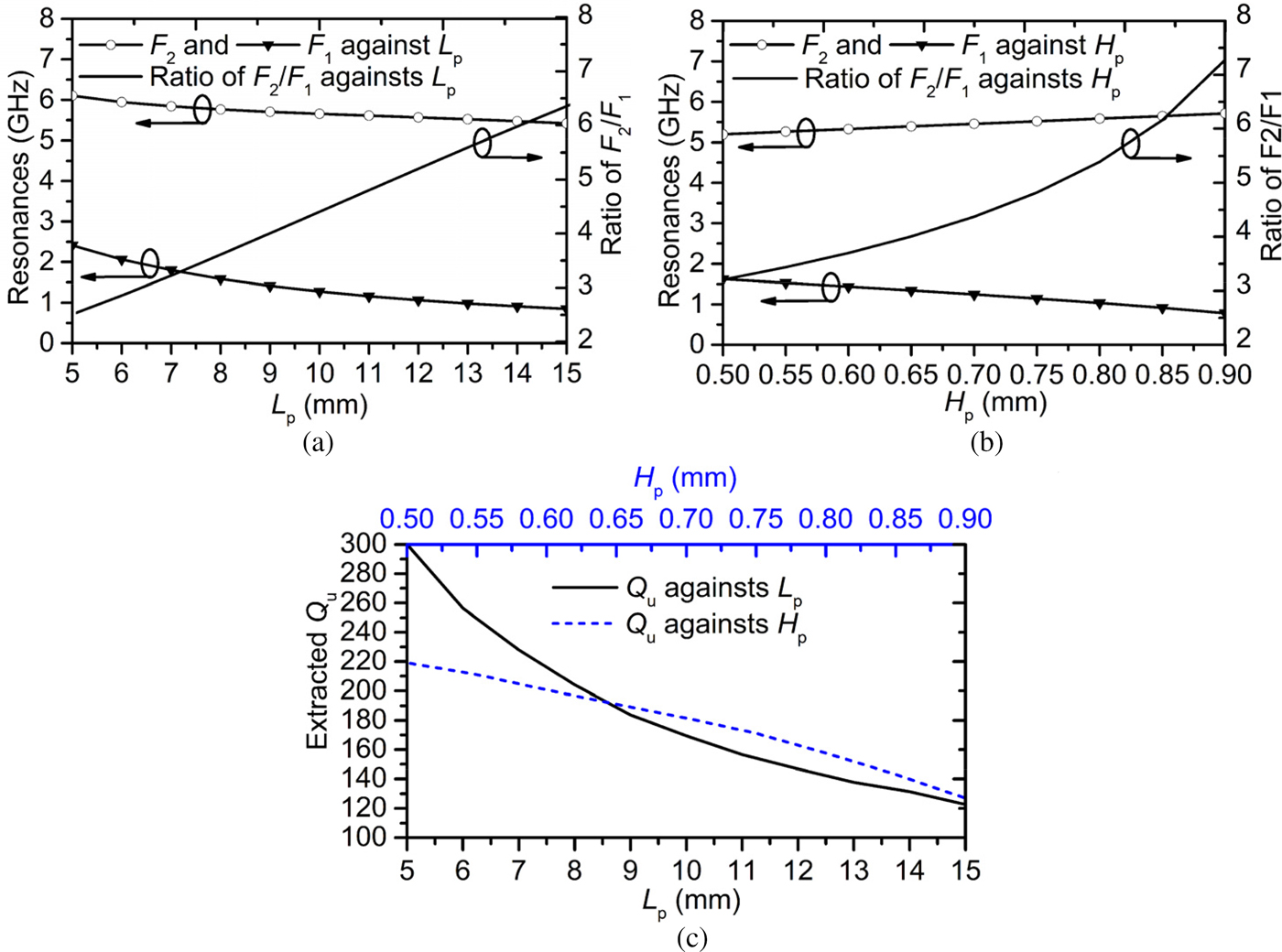
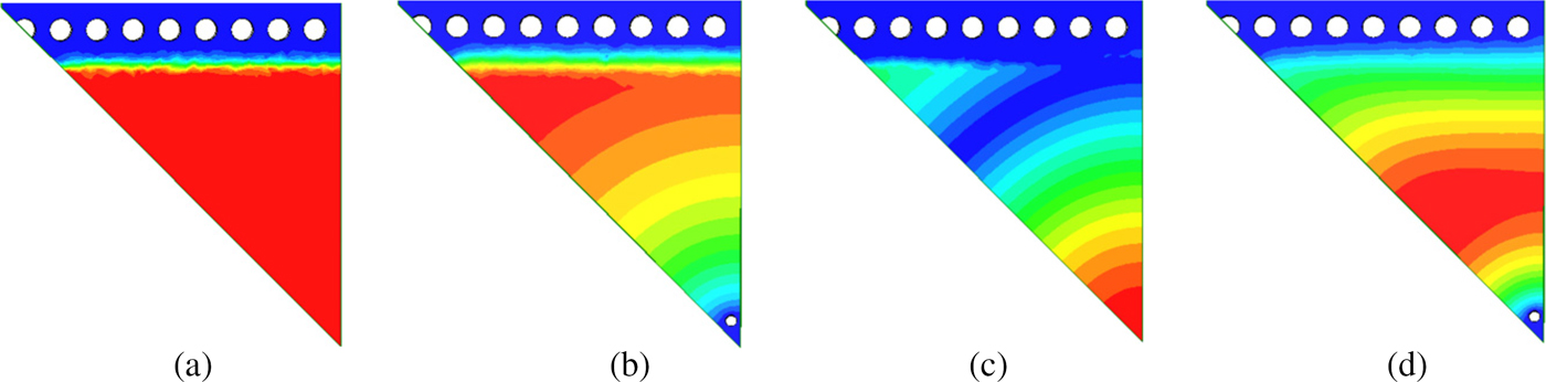
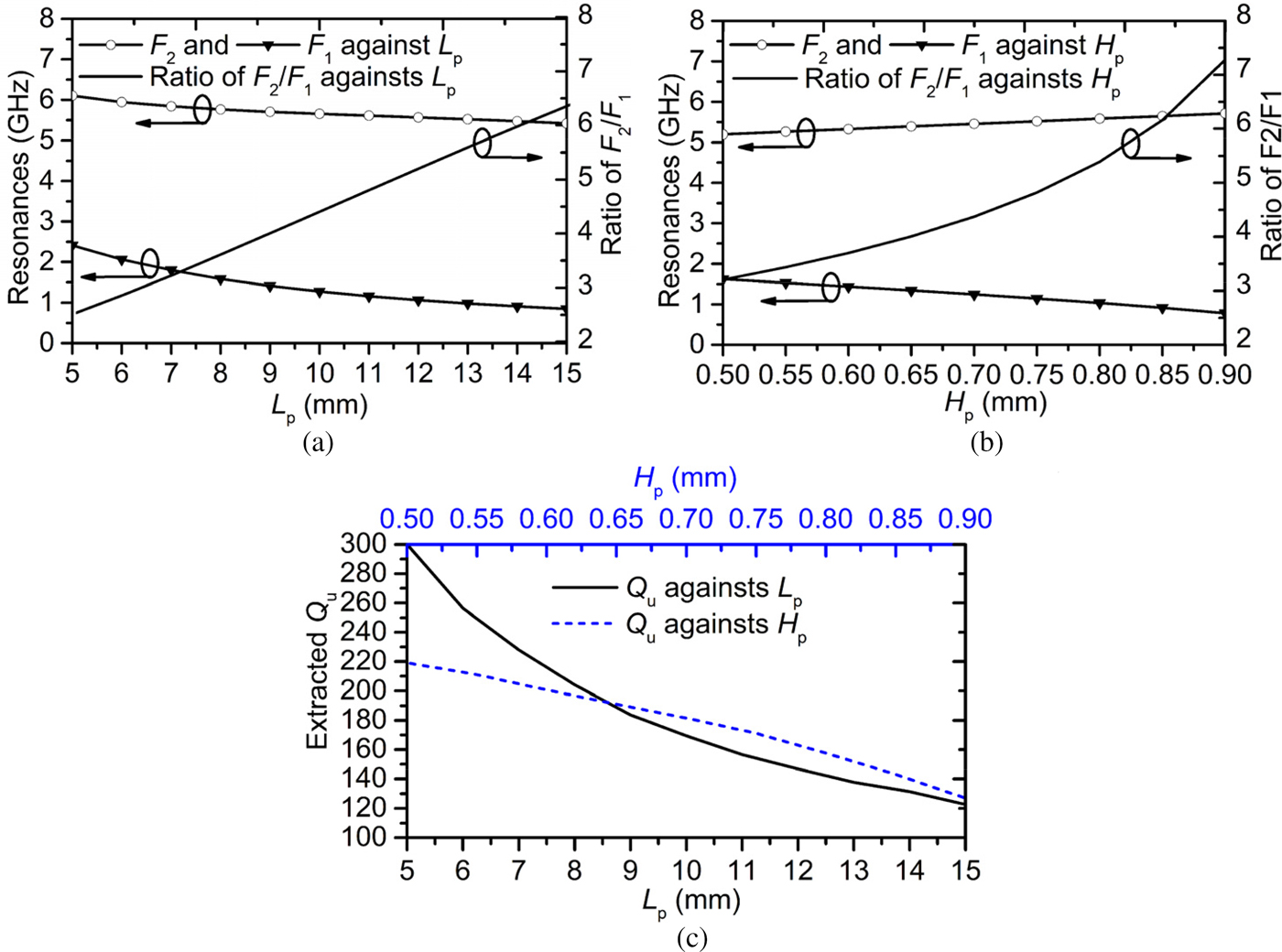
Figure 2 shows the electric field distributions of the first two resonant modes on the top and bottom metal layers of the CLEMSIW cavity. For the fundamental mode, the electric field distribution on the bottom is the same as that of a triangle patch resonator with a shorted hole, while the electric field distribution on the top layer is almost uniformly distributed above the capacitive-loaded metal patch. The thickness H P + H S of the CLEMSIW cavity is fixed by 1.041 mm. The resonances of the fundamental mode and the first higher-order mode are denoted by F 1 and F 2, respectively. As shown in Fig. 3(a), both F 1 and F 2 are shifted toward lower frequency when the size of the loaded patch is increased (i.e., increasing L p). As shown in Fig. 3(b), when H P is increased, the F 1 is decreased while F 2 is increased. The ratio of F 2/F 1 is always increased by increasing L P and H P, which can lead to a wide stopband when the CLEMSIW cavity is used to design a BPF. The size of CLEMSIW cavity can be largely reduced when compared with the full-mode SIW cavity with a loading capacitive. As shown in Fig. 3(c), unload quality factor (Q u) of the fundamental mode is also extracted by using HFSS and it is decreased by increasing L P and H P. Similarly, CLHMSIW and CLQMSIW cavities can also realize a compact size. Thus, the sizes of them are also smaller than that of the conventional SIW and EMSIW cavity counterpart, which is not analyzed again here. It should be noted that the proposed CLEMSIW cavity can be seen as a traditional EMSIW cavity with a capacitive-loaded metal patch. Thus, the formulas in [Reference Ho, Li and Chen16] can be used to approximately calculate the resonance of CLEMSIW cavity and to qualitatively explain the effect of capacitive-loaded patch. To fabricate the CLEMSIW cavity for filter's application in this paper, the H P and H S are fixed by 0.787 and 0.254 mm, respectively.
Electric fields distributions, (a) the fundamental mode on the top layer, and (b) on the bottom layer, (c) the first-order mode on the top layer, and (d) on the bottom layer.
Extracted resonances of the first two modes, (a) again L p (L 1 = 17, C P = 0.4, H P = 0.787, H S = 0.254) and (b) again H p with other parameters fixed (L 1 = 17, C P = 0.4, L P = 12, H P + H S = 1.041, units: millimeters), (c) extracted unload quality factor (Q u) of the fundamental mode with other parameters fixed.
The proposed filter and experimental results
The proposed CLEMSIW BPF
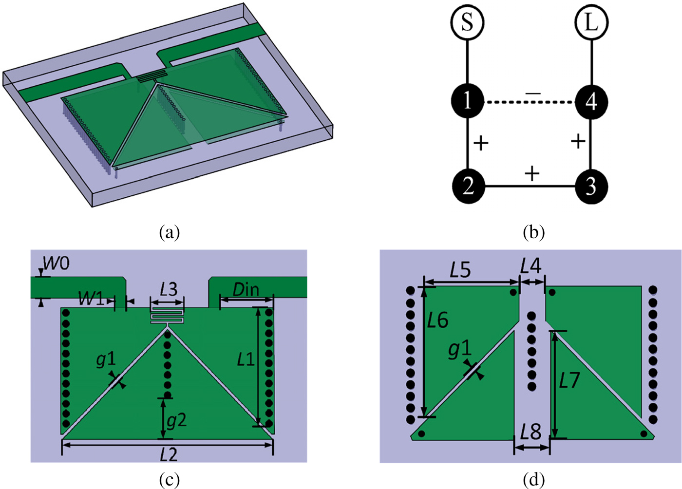
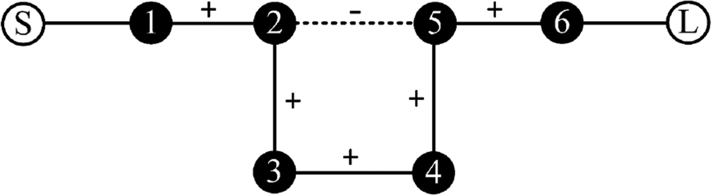
To verify the proposed CLEMSIW cavity for filter's application, a fourth-order quadruplet BPF is proposed in this part. The 3D view of the proposed BPF is shown in Fig. 4(a). The filter has two substrate layers and three metal layers. The layouts of the top and middle metal layers are shown in Figs 4(c) and 4(d), respectively. The layout of the bottom is not shown here because the bottom is always a complete metal layer. Four CLEMSIW cavities are arranged in a quadruplet scheme, and the corresponding coupling scheme is shown in Fig. 4(b).
The proposed CLEMSIW filter, (a) 3D view of the proposed filter, (b) corresponding coupling scheme, (c) layout of the top metal layer, (d) layout of the middle metal layer.

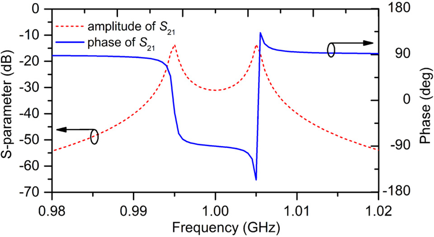
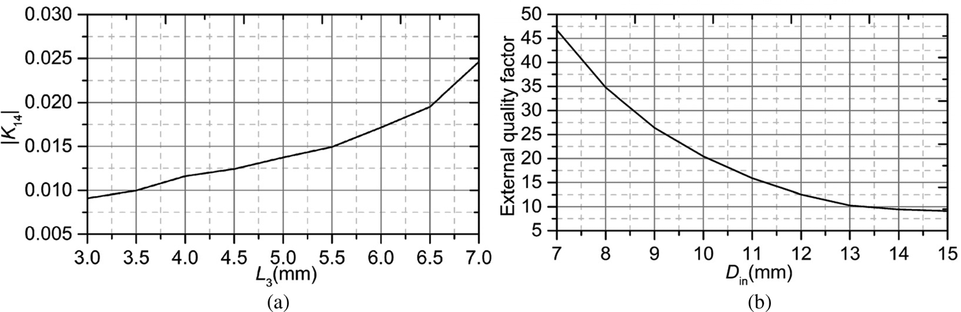
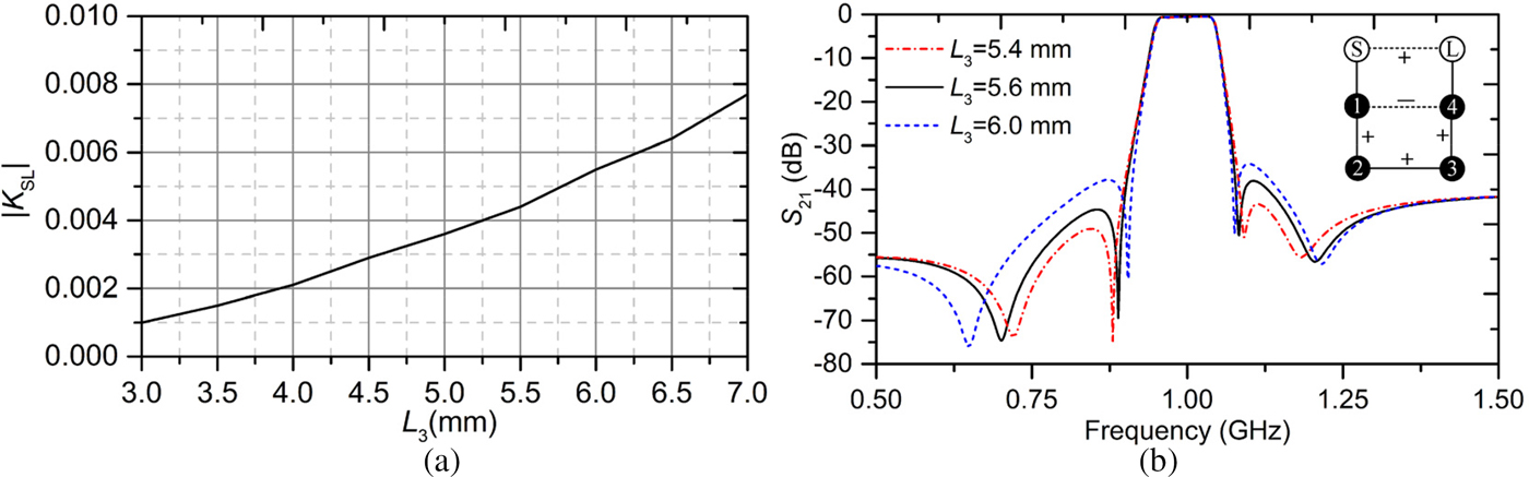
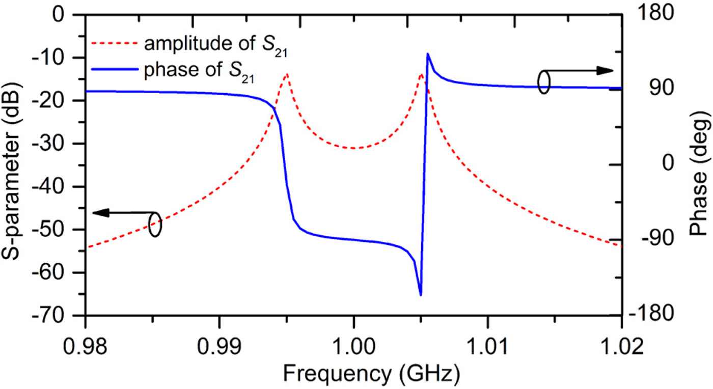
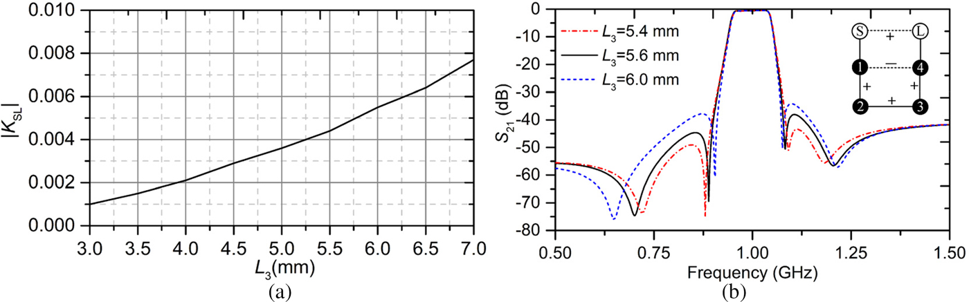
Owing to the symmetry of the proposed filter, the signs of coupling M 12 and M 34 are always the same (i.e., positive coupling). The positive sign of coupling M 23 is realized by an inductive coupling window, which is controlled by the parameter g 2. The negative coupling M 14 between cavities 1 and 4 is realized by an interdigital-like structure (the width of gap fixed by 0.12 mm, the width of metal strip line fixed by 0.3 mm, and the length of the overlapped region denoted by L 3). To realize the interdigital-like structure for the desired strength of cross-coupling path 1–4, the shape of resonators 1 and 4 is different from the shape of resonators 2 and 3, especially in the layout of adjacent area in the metal via, which results in different resonances. However, the sizes of capacitive-loaded patches can be employed to compensate the discrepancy to design a desirable passband. Simulated amplitude and phase of S 21 between the resonant nodes 1 and 4 under weak input/output coupling are extracted using HFSS and presented in Fig. 5, which has verified the achievement of negative coupling via the inter-digital capacitor [Reference Hong and Lancaster17]. The cross-coupling strength can be controlled well by the parameter L 3, and the extracted coupling coefficient |K 14| against L 3 is shown in Fig. 6(a). Tapped input and output feeding lines are coupled to the first and fourth CLEMSIW cavities, respectively, and offset D in is employed to control the external quality factor (Q e). The extracted Q e against D in is shown in Fig. 6(b). Because the physical size of the proposed CLEMSIW cavity is much smaller than waveguide wavelength at the operating frequency, the tapped input/output feeding line and CLEMSIW cavity with the periodic metal holes will lead to an inductive SL coupling. Thus, the proposed filter structure may realize four imaginary-axis FTZs. To eliminate the effect of the resonance, CLEMSIW cavities 1 and 4, the metal vias connecting the bottom and loaded metal patches, are removed to extract the equivalent S–L coupling coefficient. As shown in Fig. 7(a), the equivalent S–L coupling strength K SL is extracted by using HFSS and the following formula (1) [Reference Hong and Lancaster17]:
 $$KSL{\rm}={\rm } \displaystyle{{1{\rm -}\sqrt {1{\rm -}{\vert {S21} \vert } ^2}} \over {\vert {S21} \vert }}, $$
where the |S 21| is the amplitude of S 21 at the center frequency of 1 GHz. The K SL is increased when the parameter L 3 is increased. However, the S–L coupling may not be easily controlled independently from the cross-coupling K 14 because both K SL and K 14 are dependent on the inter-digital structure, i.e., the parameter L 3. To further illustrate the existence of S–L coupling, simulated responses with different parameter L 3 based on the proposed filter in Fig. 4(a) are shown in Fig. 7(b). Four FTZs are produced, and the locations of them can be tuned by the parameter L 3. Thus, the coupling scheme of the proposed filter in Fig. 4(a) can be modeled by a quadruplet with S–L coupling when the four FTZs close to the passband are considered. The revised coupling scheme is shown in the insertion in Fig. 7(b).
Simulated amplitude and phase of S 21 between the resonant nodes 1 and 4 under weak input/output coupling (L 1 = 17, L 3 = 4.5, C P = 0.4, L P = 15, units: millimeter).
Extracted coupling coefficients, (a) cross-coupling coefficient |K 14|, and (b) external quality factor (L 1 = 17, C P = 0.4, L P = 15, units: millimeter).

S–L coupling and simulated responses, (a) extracted S–L coupling coefficient at the center frequency, (b) simulated responses adjusted by the design parameter L 3 (g 1 = 0.42, g 2 = 6.25, L 1 = 18.3, L 2 = 33, L 3 = 5.15, L 4 = 3.5, L 5 = 13.35, L 6 = 17.8, L 7 = 15.05, units: millimeters).
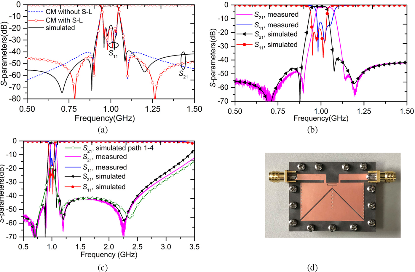
Because the S–L coupling is dependent on the cross-coupling M 14, two FTZs produced by the cross-coupling path 1–4 can be synthesized to approximately design the proposed filter. To illustrate the proposed filter, a prototype filter was synthesized with the specifications, i.e., f 0 of 1 GHz, FBW of 10%, and return loss (RL) of 20 dB; and two normalized FTZs at −2.5i and 2.5i in S-domain were considered. The corresponding coupling matrix (CM) based on the coupling scheme in Fig. 4(b) is shown in (2). Based on the synthesized method in [Reference Hong and Lancaster17], the initial structure can be obtained; finally, the HFSS is employed to optimize the desired responses. The simulated responses are compared with the synthesized responses with two FTZs in Fig. 8(a). For comparison, the filter was also synthesized with four FTZs (−2.5i, 2.5i, −6i, and 6i in S-domain), and the corresponding CM based on the coupling scheme in the insertion in Fig. 7(b) is shown in (3). The synthesized responses are also presented in Fig. 8(a). The discrepancy of the cross-coupling coefficients M 14 based on the two cases in (2) and (3) is <11.7%, and the discrepancy of main coupling coefficients is <0.55%. Thus, we can consider two controllable FTZs to design the proposed filter. From the simulated responses in Fig. 8(a), four FTZs are simulated at 0.704, 0.881, 1.08, and 1.197 GHz. The first and fourth FTZs are asymmetrical about the passband, which may be attributed to the dispersive S–L coupling [Reference Szydlowski, Lamecki and Mrozowski18]. The main dimensions of the structure are given as follows: W 0 = 3.18, W 1 = 1, g 1 = 0.42, g 2 = 6.25, L 1 = 18.3, L 2 = 33, L 3 = 5.15, L 4 = 3.5, L 5 = 13.35, L 6 = 17.8, L 7 = 15.05, D in = 12.25 (units: millimeters).
 $$\left[ {\matrix{ 0 & {{\rm 1}{\rm. 0279}} & 0 & 0 & 0 & 0 \cr {{\rm 1}{\rm. 0279}} & 0 & {{\rm 0}{\rm. 8884}} & 0 & {{\rm -0}{\rm. 1026}} & 0 \cr 0 & {{\rm 0}{\rm. 8884}} & 0 & {{\rm 0}{\rm. 7408}} & 0 & 0 \cr 0 & 0 & {{\rm 0}{\rm. 7408}} & 0 & {{\rm 0}{\rm. 8884}} & 0 \cr 0 & {{\rm -0}{\rm. 1026}} & 0 & {{\rm 0}{\rm. 8884}} & 0 & {{\rm 1}{\rm. 0279}} \cr 0 & 0 & 0 & 0 & {{\rm 1}{\rm. 0279}} & 0 \cr}} \right]$$
 $$\left[ {\matrix{ 0 & {{\rm 1}{\rm. 0269}} & 0 & 0 & 0 & {{\rm 0}{\rm. 0031}} \cr {{\rm 1}{\rm. 0269}} & 0 & {{\rm 0}{\rm. 8859}} & 0 & {{\rm -0}{\rm. 1161}} & 0 \cr 0 & {{\rm 0}{\rm. 8859}} & 0 & {{\rm 0}{\rm. 7449}} & 0 & 0 \cr 0 & 0 & {{\rm 0}{\rm. 7449}} & 0 & {{\rm 0}{\rm. 8859}} & 0 \cr 0 & {{\rm -0}{\rm. 1161}} & 0 & {{\rm 0}{\rm. 8859}} & 0 & {{\rm 1}{\rm. 0269}} \cr {{\rm 0}{\rm. 0031}} & 0 & 0 & 0 & {{\rm 1}{\rm. 0269}} & 0 \cr}} \right]$$
Simulated, synthesized, and measured results, (a) simulated and synthesized responses, (b) simulated and measured results, (c) wideband responses, (d) photograph of the fabricated filter.

Experimental results
To verify the proposed structure, the designed CLEMSIW filter was fabricated and measured. The comparison between the simulated and measured responses is shown in Fig. 8(b). The measured results agree well with the simulated ones. The measured f 0 and 1 dB passband bandwidth of the BPF are 1.022 GHz and 85.3 MHz, respectively. The measured f 0 is slightly larger than the simulated one, which may be attributable to the actual ε r and machining error. The insertion loss (IL) of the passband is 1.55 dB, and the RL within the passband is above 12.5 dB. Four FTZs (0.705, 0.897, 1.142, and 1.197) are observed as expected. S-parameter responses simulated and measured in a wide frequency band are presented in Fig. 8(c). An extra FTZ is measured at 2.251 GHz (simulated at 2.275 GHz), which can further improve the out-of-band performances. The additional FTZ may be produced by the weak dispersive S–L coupling [Reference Szydlowski, Lamecki and Mrozowski18]. The out-of-band rejection lever over 40 and 20 dB is better than 2.53 and 3.26 GHz (i.e., 2.476f 0 and 3.19f 0), respectively. The size of the designed filter is 35 mm × 26 mm (0.123λ g × 0.092λ g), where λ g is the guided wavelength at f 0. To further verify a parasitic dispersive S–L coupling in the proposed filter, the coupling path between cavities 1 and 4 is simulated with the second and third cavities in the proposed filter removed. The simulated S 21 is shown in Fig. 8(c), and three FTZs are produced by the coupled cavities 1 and 4, which can verify the existence of parasitic dispersive S–L coupling producing three extra FTZs. The photograph of the fabricated filter is shown in the insertion in Fig. 8(d).
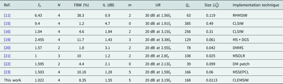
A comparison between the designed filter and other reported size-reduced SIW filters as well as various microstrip filters in the literature is presented in Table 1. Compared with SIW filters or microstrip filters, the proposed filter has the merits of smaller size, more FTZs, and wider stopband. Moreover, the designed filter also has good Q u except for the merit of smaller size when compared with high-performance microstrip filters using various techniques, such as the hybrid of microstrip and DGS [Reference Luo, Ma and Li19], dual-mode microstrip structure [Reference Gorur20], concentric microstrip open-loop resonators [Reference Athukorala and Budimir21], dual-mode patch [Reference Tu and Chang22], and microstrip short-ended parallel-coupled line [Reference Lin23].
Comparison with other reported size-reduced SIW filter

f 0, center frequency/GHz; N, order of filter; λ g, guide wavelength at f 0; m, number of FTZs; IL, insertion loss/dB; UR, upper stopband performance; Q u, measured unloaded quality factor; MS, microstrip; DGS, defected ground structure; DM, dual-mode; MSOLR, microstrip open-loop resonators; MSSEPCL, microstrip short-ended parallel-coupled line.
Discussions
In this paper, one filter was designed to verify the proposed size-reduced CLEMSIW cavity, but the measured results can verify the feasibility of the proposed CLEMSIW cavity for designing filters with high performances. Moreover, higher-order filters may be designed by using the proposed CLEMSIW cavities based on the concept in [Reference Hong and Lancaster24]. For example, a sixth-order filter can be designed based on the proposed fourth-order filters. Two new CLEMSIW cavities are coupled to the input and output resonators (i.e., the first and fourth CLEMSIW cavities) of the layout in Fig. 4, respectively, and then the two added CLEMSIW cavities become the new input and output resonators, respectively. The corresponding coupling scheme is shown Fig. 9. This sixth-order filter can realize a quasi-elliptic response with two symmetric FTZs in theory. When the cross-coupling path 2–4 or 3–5 in the coupling scheme in Fig. 9 is realized, two lower or two upper stopband FTZs can be produced [Reference Thomas25]. An embedded strip line between the two non-adjacent CLEMSIW cavities 2 and 4 (or cavities 3 and 5) may be employed to realize the desired cross-coupling path [Reference Gong, Hong, Zhang, Chen and You26].
The coupling scheme of the sixth-order filtering function.

Furthermore, the CLEMSIW cavity has the smallest size when compared with the CLHMSIW and CLQMSIW cavities, but the Q u of CLHMSIW and CLQMSIW cavities may be larger than that of CLEMSIW cavity. Thus, the technique based on combining the equivalent magnetic boundary conditions and the pedestal SIW cavity with a loaded metal patch can be further exploited to design high-performance filters, such as size-reduced CLHMSIW and CLQMSIW filters.
Conclusion
In this paper, a novel fourth-order quadruplet BPF is proposed based on the novel size-reduced EMSIW cavities. The EMSIW cavity is constructed by the conventional EMSIW cavity with a capacitive-loaded metal patch. The characteristics of the CLEMSIW cavity are analyzed in detail. For the demonstration, the designed filter was fabricated and measured. The measured results agree with the simulated ones, which verify the feasibility of the proposed filter. The proposed filter has the merits of smaller size, more FTZs, and wider stopband.
 Qing Liu was born in 1991. He received the B.S. degree in communications engineering from the Hunan University, Changsha, China, in 2014, and received the M.S. degree in electronic science and technology from the National Digital Switching System Engineering and Technological Research Center, Zhengzhou, China, in 2017, where he is currently pursuing the Ph.D. degree in information and communication engineering. His current research interests include microwave filters and passive components.
 Dongfang Zhou was born in 1963. He received the Ph.D. degree from the Zhejiang University, Hangzhou, China. He is currently working at the National Digital Switching System Engineering and Technological Research Center, Zhengzhou, China. His current research interests include antenna and propagation, radio frequency and microwave circuits and systems, high-power microwave and radome.
 Dewei Zhang was born in 1973. He received the Ph.D. degree from the National Digital Switching System Engineering and Technological Research Center, Zhengzhou, China, in 2005. He is currently working at the National Digital Switching System Engineering and Technological Research Center. His current research interests include RF/microwave devices, such as antennas, filters, and power amplifier, for wireless communications and radar systems.
 Chenge Bian was born in 1996. He received the B.S. degree in information engineering from the Xi'an Jiaotong University, Xi'an, China, in 2018. He is currently pursuing the M.S. degree in the National Digital Switching System Engineering and Technological Research Center, Zhengzhou, China. His current research interests include microwave filters and passive components.
 Yi Zhang was born in 1980. He received the Ph.D. degree in electronic engineering from the Tsinghua University, Beijing, China, in 2015. He is currently working at the National Digital Switching System Engineering and Technological Research Center, Zhengzhou, China. His current research interests include microwave passive components, antennas, metamaterials, and applications.