I. INTRODUCTION
In the last decades, lead zirconate (PbZrO3)-based antiferroelectric (AFE) materials have received an increasing attention for their potential application in microelectromechanical system.Reference Lu, Chu, Yang and Huang1 Compared with the linear dielectric (DE) materials and ferroelectric (FE) materials, AFEs usually show higher energy storage density owning to their large saturated polarization and nearly zero remnant polarization. Moreover, AFEs also possess fast charge–discharge speed and good fatigue endurance.Reference Chen, Zhang, Cao, Wang, Dong and Gu2, Reference Zhang, Chen, Cao, Wang and Dong3 Thus, AFEs are more suitable for application in pulsed capacitors with high-energy density. So far, the studies on the energy storage performance in AFEs are mainly concerned with thin films (<1 μm) and bulk ceramics.Reference Ma, Kwon, Narayanan and Balachandran4–Reference Burn7 However, due to the lower breakdown field (less than 100 kV/cm), the obtained energy storage density in AFE bulk ceramics was usually very small. The maximum reported value was only about 2 J/cm3 at present.Reference Burn7 Although AFE thin films possessed a higher breakdown field (about 1000 kV/cm), the overall stored energy was limited owing to their thinner thickness, which also prevented their application in practice. Therefore, AFE thick films (>1 μm) with dense microstructure should avoid the disadvantages of AFE thin films and bulk ceramics and are more likely to be used in high-energy storage capacitors.
It is generally believed that the sol–gel is a more promising way to deposit AFE and FE thick films with uniform and dense microstructure, although several techniques, such as sol–gel, screen printing, tap casting, and electrophoretic deposition method, have been used to fabricate thick films.Reference Iijima, Osone, Shimojo and Nagai8 Moreover, it was reported that the orientation and microstructure of lead-based FE and AFE films were heavily effected by the lead content.Reference Wu, Zhu, Xiao, Zhu, Tan and Zhang9–Reference Xu, Eric Cross and Ravichandran12 In Xu’s investigation, Pb0.99Nb0.02(Zr0.85Sn0.13Ti0.02)0.98O3 and Pb0.97La0.02(Zr0.65Sn0.31Ti0.04)O3 AFE thick films with dense microstructure were successfully prepared by the addition of PbO insert layers.Reference Xu, Ye and Eric Cross11, Reference Xu, Eric Cross and Ravichandran12 However, in his investigation, the energy storage behavior was not studied.
Therefore, in this work, typical Pb0.97La0.02(Zr0.98Ti0.02)O3 (hereafter abbreviated as PLZT) AFE thick films were prepared by the sol–gel method. To prevent the crack formation and offset the lead loss during the heat treatment, different PbO insert layers were also added. The effects of PbO insert layer on the microstructure and energy storage performance of AFE thick films were investigated systemically.
II. EXPERIMENTAL PROCEDURE
PLZT AFE thick films were prepared by the sol–gel technique. Lead acetate trihydrate, lanthanum acetate, zirconium propoxide, and titanium isopropoxide were used as the raw materials. Acetate was selected as a solvent. To compensate the lead loss during annealing and to prevent the formation of a pyrochlore phase, 20% excess lead was added in the precursor. The concentration of the final solution was about 0.5 M. More detailed description on the synthesis of the sol could be found in our recent work.Reference Hao, Yue, Xu, An and Nan13 The conductive LaNiO3 films with a thickness of about 150 nm were selected as bottom electrodes, which was prepared on Si(100) substrates from the chemical solution deposition route and was similar to Ref. Reference Hao and Zhai14. It should be noted that the obtained LaNiO3 films showed the random growth orientation with weak diffraction peaks.
The PLZT solution was aged for 24 h before use. PLZT AFE films were prepared through a multiple-layer spin-coating technique at 3000 rpm for 40 s. Each as-deposited PLZT layer was first dried at 350 °C for 10 min and then pyrolyzed at 550 °C for 10 min. After every four PLZT coatings, a layer from PbO solution was coated and then annealed at 700 °C for 10 min. For comparison, here, PbO solutions with three different concentrations of 0, 0.2, and 0.4 M/L were selected. Zero mole per liter meant that no PbO layer was added. After 12 PLZT coating layers were deposited on LaNiO3 bottom electrodes under the same heat treatment process but with different PbO insert layer, a 0.8-M/L PbO capping layer was subsequently coated and then annealed at 700 °C for 30 min to crystallize completely. These PbO layers served the purposes of preventing excessive lead loss and forming a pure perovskite phase with crack-free microstructure. For convenience, PLZT samples with the PbO insert layer from 0, 0.2, and 0.4 M/L solutions were labeled as PLZT-0, PLZT-2, and PLZT-4, respectively. The final thickness for all the PLZT thick films was about 2.0 μm, which were determined by the cross-sectional pictures. It should be noted that all the PbO solutions were prepared from lead acetate trihydrate and acetic acid, and that the teat treatment processes were fulfilled in a tubular resistance furnace.
The phase composition and surface morphology of PLZT AFE films were obtained via x-ray diffraction (XRD) and scanning electron microscopy (SEM), respectively. For the measurements of electrical properties, gold pads of 0.2 mm in diameter were coated on the surface as top electrodes by dc sputtering. The frequency- and temperature-dependent DE properties of the AFE films were measured using a Tonghui TH2828 Precision LCR meter (Tonghui Electronics Co., Ltd., Changzhou, China). The polarization–electric field hysteresis (P–E) loops of PLZT AFE thick films were measured at 1 kHz and at different temperature by a Radiant Technology Ferroelectric tester (Radiant Technologies, Inc., Albuquerque, NM). The energy storage performance was calculated according to the P–E results.
III. RESULTS AND DISCUSSION
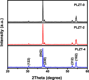
Figure 1 shows the XRD patterns of PLZT AFE thick films with different PbO insert layer. It should be noted here that PLZT films with present chemical composition were orthorhombic AFE phase. Thus, the lattice indexes of the peaks were labeled accordingly.Reference Lanagan, Kim, Jang and Newnham15 As shown in this figure, all the samples had crystallized into a pure perovskite phase after annealed at 700 °C. All the AFE films displayed a (042)-preferred orientation, and no obvious difference in the XRD curves was detected. Moreover, although excessive lead content was added, no secondary phase such as PbO was formed. These results demonstrated that the phase structure of the thick films was slightly affected by the PbO insert layer. The (042)-preferred orientation was supposed to be caused by the LaNiO3 bottom electrodes and the multistep heat treatment procedure. It was reported that the polar direction in induced FE phase was along <042> plane, corresponding to the pseudocubic <111>.Reference Shirane and Hoshino16 So it could be concluded that AFE materials along this plane have larger polarization values, which in turn lead to the improvement in energy storage performance.
XRD pattern of PLZT AFE thick films.

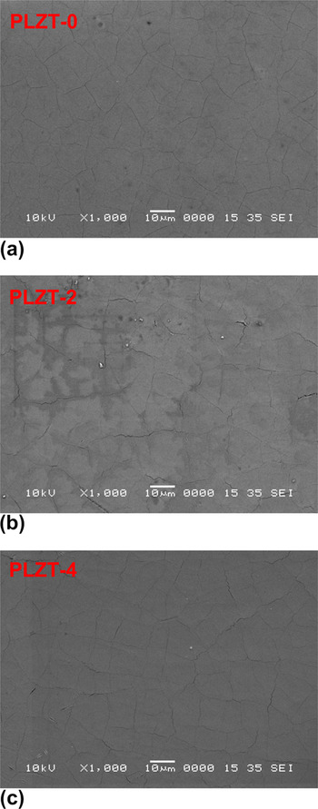
The surface microstructure images of PLZT AFE thick films are presented in Fig. 2. It could be found in this figure that all the samples showed a uniform surface structure with some cracks. Clearly, just as the XRD curves, the SEM images of the thick films were also little affected by the PbO insert layer. Comparatively, PLZT films with 0.4-M/L PbO insert layer were denser. Therefore, the microstructure of AFE thick films could be improved by the addition of proper PbO insert layer. Based on these results, it could be concluded that the growth process of the films was not obviously changed by the PbO insert layer.
Surface SEM micrographs of PLZT AFE thick films.

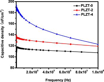
The capacitance densities of the three PLZT thick films are revealed in Fig. 3, which were measured at room temperature in the frequency of 1–1000 kHz. As expected, the capacitance per area for all the samples was decreased gradually as the frequency increasing. The capacitance density in our films is smaller in contrast to lead-based FE thin films, in which a maximum value of about 1000 nF/cm2 could be obtained.Reference Brenneckal, Ihlefeld, Maria, Tuttle and Clem17 The small capacitance density in this work was mainly caused by the higher thickness of our films. Meanwhile, the AFE films often have a smaller DE constant, which in turn also leads to a smaller capacitance density. It could be clearly observed that the capacitance density of the PLZT films was increased by the PbO insert layer with higher concentration solution. For example, the capacitance density at 10 kHz was 186.3, 126.9, and 115.9 nF/cm2 for PLZT-4, PLZT-2, and PLZT-0, respectively. This result indicated that, although their phase structure and surface microstructure were not evidently influenced by the PbO insert layer, the DE properties of the AFE thick films could be greatly improved. Thus, it could be concluded that the PbO insert layer mainly took the function of compensation the lead loss during the heat treatment procedure. Accordingly, the little deficiency in the thick films made the enhancement of polarization behavior, which would in turn lead to the improvement of energy storage performance, as shown in the following part.
The capacitance density of PLZT AFE films as the function of frequency.

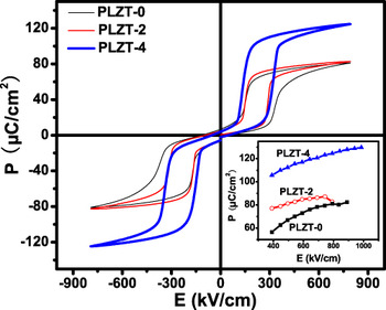
To study the PbO insert layer-dependent phase switching behaviors of PLZT AFE films, P–E loops were measured at 1 kHz and at room temperature, as shown in Fig. 4. The electric field was slowly stepped in a cyclic manner from 0 to E max, then E max to −E max and −E max to 0. The double hysteresis loops demonstrated the AFE nature of all the PLZT thick films at room temperature. A small remnant polarization was also observed in these samples, which was supposed to be caused by the interface layer, space charge, some unstable AFE regions, and so on. From this figure, two evident characteristics could be found. For one thing, the polarization ability and the squared degree of hysteresis loop were greatly enhanced by the addition of 0.4-M/L PbO insert layer. The insert in Fig. 4 presents the maximum polarization values of these AFE films, as a function of applied electric field up to their breakdown values. Clearly, PLZT films with 0.4-M/L PbO insert layer not only had the largest saturation polarization but also possessed the highest breakdown field. For example, the values of the saturation polarization at an applied electric field of 791 kV/cm were 124.6, 82.6, and 81.0 μC/cm2 for PLZT-4, PLZT-2, and PLZT-0, respectively. The improved field endurance of PLZT films with 0.4-M/L PbO insert layer was mainly contributed to their denser surface microstructure. For another, the PbO insert layer had no obvious effect on the phase transformation fields of the AFE thick films and all the samples shared the similar critical fields. By extrapolating the two steepest sections of the hysteresis loops and obtaining their intersections with the horizontal axis, the obtained forward (AFE to FE) switching field E AFE–FE and backward (FE to AFE) switching field E FE–AFE were about 280 and 105 kV/cm, respectively.
The room temperature P–E loops of PLZT thick films measured at 1 kHz and at 791 kV/cm. The insert is the electric field-dependent saturation polarization of the PLZT films.

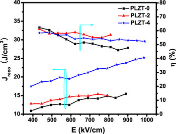
Figure 5 illustrates the electric field-dependent energy storage performance of the PLZT AFE films, which were measured at room temperature and up to their breakdown field. According to the definition of energy storage density  (E = applied electric field and P = polarization) by P–E loops,Reference Chu, Zhou, Ren, Neese, Lin, Wang, Bauer and Zhang18 the recoverable energy density J reco, the energy loss density J loss, and energy efficiency η (η = J reco/(J reco + J loss)) were calculated. It should be noted here that only part of the stored energy could be released during the depolarization process. The unreleased energy was mainly caused by the hysteresis loss during the phase transformation between the AFE and FE state. As expected, the recoverable energy density J reco for all the thick films were gradually increased as the increase of applied fields. Moreover, in the measurement range, the J reco values for PLZT films with the addition of 0.4-M/L PbO insert layer were much higher, as compared with other samples. It was consistent with results obtained in Fig. 4. For example, the values of J reco measured at E = 791 kV/cm and at room temperature were 22.3, 15.0, and 14.9 J/cm3 for samples PLZT-4, PLZT-2, and PLZT-0, respectively. The maximum J reco value of 25.2 J/cm3 was obtained in the sample PLZT-4 at its critical breakdown field of 984 kV/cm at room temperature. Different from energy storage density, the energy storage efficiency was less affected by the PbO insert layer. The η values were similar for the three samples and were slightly declined as the measurement field increasing. The η value for sample PLZT-4 was changed from 58.3% to 52.3% as the electric field increased from 393 to 984 kV/cm.
The electric field-dependent energy storage density and energy storage efficiency curves of the PLZT thick films measured at room temperature and up to their critical breakdown field.

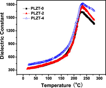
The temperature-dependent DE constant of the three samples is plotted in Fig. 6, which was measured at 100 kHz and on heating process. Clearly, all the curves displayed the same tendency. Namely, with the temperature increasing, the DE constant was first increased gradually and then decreased. All the AFE films got their DE peak at 235 °C, which was the so-called Curie temperature (T c). The DE constant for sample PLZT-4, PLZT-2, and PLZT-0 was 1823, 1778, and 1623 at T c, respectively. It should be noted that the only DE peak was caused by the transition from FE to paraelectric (PE) phase. Based on the previous investigations, as the temperature increasing, AFEs with orthorhombic structure experienced a transformation from AFE to FE, then to PE state.Reference Dobal, Katiyar, Bharadwaja and Krupanidhi19 However, the AFE–FE phase transition in the temperature–DE constant curves usually could not be detected in film form.
Temperature dependence of the DE constant of the PLZT thick films measured at 100 kHz and on heating process.

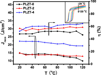
To investigate the temperature-dependent stability of the capacitors, the energy storage density and the energy storage efficiency measured at 791 kV/cm in the temperature ranging from 20 to 120 °C are presented in Fig. 7. Evidently, in the measurement range, all the curves were only slightly varied, indicating good temperature stability in the energy storage performance. As the temperature increasing, the J reco values were slightly decreased, while the η values showed an increasing tendency. The highest values of J reco and η were obtained in sample PLZT-4. For instance, the η value for PLZT-4 was changed from 52.3% to 64.7% with the operating temperature ranging from 20 to 120 °C. This phenomenon was mainly caused by the decrease in the saturation polarization and the forward switching field E AFE–FE as the operating temperature increasing, as shown in the insert in Fig. 7. However, the temperature had nearly no influence on the backward switching field E FE–AFE, which held constant in the measurement range. Accordingly, the both values of J reco and J loss were reduced as the temperature increasing, but the declined degree in J loss was more evident.
Temperature dependence of energy storage density and energy storage efficiency of the PLZT thick films measured at 1 kHz.

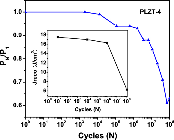
The higher polarization–fatigue endurance was also necessary for the application of AFE thick films in capacitors. Hence, the fatigue behavior of PLZT-4 AFE thick films was investigated, as shown in Fig. 8, which was measured at 400 kV/cm at room temperature. Here, P N denoted the value saturation polarization after N-switching cycles. After 106 and 108 switching, the reduction of P N was 6.5% and 37%, respectively, which was close with our previous results obtained in AFE thin films.Reference Hao, Zai and Yao20 The insert in Fig. 8 gives the corresponding recoverable energy storage density as a function of switching cycles. After 106 switching, the J reco value was only declined from 17.5 to 16.1 J/cm3, indicating good fatigue endurance.
The electric field dependence of polarization fatigue properties of PLZT films coated by 0.4-M/L PbO insert layer measured at 400 kV/cm and at room temperature. The insert shows the energy storage density of this film after different switching cycles.

IV. SUMMARY
In conclusion, the effects of PbO insert layer on the microstructure and the energy storage behaviors of the PLZT AFE thick films were investigated in detail. It was found that the PbO insert layer had slightly affected on the growth process of the films. All the films showed a (042)-preferred orientation with uniform microstructure. However, the PbO insert layer had strong influence on the DE properties and the energy storage performance. The DE constant of the PLZT films was increased by the PbO insert layer. At the same time, as the concentration of solutions for PbO insert layer increased from 0 to 0.4 M/L, the saturation polarization and critical breakdown field were greatly improved. As a result, the best energy storage performance was obtained in 0.4-M/L PbO-inserted PLZT AFE thick films. The highest energy storage density and efficiency were 25.2 J/cm3 and 52.3% measured at 984.8 kV/cm, respectively. Moreover, it was found that this AFE thick film also showed good fatigue performance. In a word, it was an efficient way to optimize the energy storage performance by the addition of proper PbO insert layer.
ACKNOWLEDGMENTS
The authors would like to acknowledge the financial support from the National Natural Science Foundation of China under Grant No. 51002071, the Natural Science Foundation of Inner Mongolia under Grant No. 2010BS0802, the Opening Project of Xinjiang Key Laboratory of Electronic Information Materials and Devices under Grant No. XJYS0901-2011-01, the Innovation Fund of Inner Mongolia University of Science and Technology under grant no. 2009NC007, and the Fund of Industry-Academia-Research Project of Inner Mongolia University of Science and Technology under Grant No. PY-201003.