Introduction
Microelectromechanical systems (MEMS) devices are being continually pushed in the direction of smaller size and increased integration density with a faster, larger range of motion and more powerful actuating elements. Currently, this is accomplished by incorporating passive mechanical elements with nanoscale dimensions within larger MEMS devices driven electrostatically. In this scheme, silicon is only a structural material driven by forces that are external to it. Incorporation of active materials directly into the nanoelectromechanical systems (NEMS) structure enables direct coupling of the mechanical deformation to the internal electric fields for nanomechanical actuation and for generation of electrical signals in response to ultrasmall mechanical displacements.Reference Uchino1–Reference Isarakorn, Sambri, Janphuang, Briand, Gariglio, Triscone, Buy, Reiner, Ahn and de Rooij6 In this case, the sensing and actuating can be combined into the same system using piezoelectric materials.
Piezoelectricity is an intrinsic, electromechanical coupling phenomenon arising from the non-centrosymmetric arrangement of atoms within the unit cell. Piezoelectric materials develop surface charges in response to an applied pressure (direct effect) and create mechanical displacements in response to an applied electric field (converse effect), which are useful for sensors and actuators, respectively. These active materials are highly desirable for a number of reasons. An integrated piezoelectric spring element, for example, cantilever-type devices, can generate a large force with a small applied voltage in a linear fashion. This decreases the complexity, retains the integration density, and reduces the voltage burden on the integrated control electronics. In addition, robustness comes from the fact that high electric fields are confined inside solid-state materials. In MEMS actuators, a piezoelectric drive is always beneficial at low voltages compared to an electrostatic approach, as the force per unit area is linear in an electric field (V/thickness) for the piezoelectric drive and quadratic for the electrostatic approach.Reference Trolier-McKinstry and Muralt3–Reference Muralt, Polcawich and Trolier-McKinstry5
Applications of piezoelectric materials in MEMS structures typically take advantage of particular piezoelectric response modes, identified by numerical subscripts indicating the axis of the applied field and the axis of the strain or stress response.Reference Uchino1, Reference Trolier-McKinstry and Muralt3 For instance, a strain induced in the same direction as an applied electric field is labeled as “33,” and a strain induced in a direction transverse to the applied electric field is labeled “31.” These are quantified with piezoelectric coefficients relating the strain to the applied electric field (d coefficients) and stress to the applied electric field (e coefficients). Thin films are also constrained by the boundary conditions imposed by the substrate. These effects are captured by effective piezoelectric coefficients for thin films, e 31,f relating in-plane stress to out-of-plane electric field, and d 33,f, relating out-of-plane strain to out-of-plane electric field.Reference Trolier-McKinstry and Muralt3 Both of these responses have been successfully applied in cantilever-type piezoelectric MEMS. For example, vertical capacitor structures with top and bottom electrodes allow the implementation of 31 responses, while the interdigitated electrodes on the top surface permit 33 responses. Both responses are directly measureable and are used to characterize piezoelectric thin-film response for MEMS structures.
Piezoelectric MEMS
Piezoelectric materials have previously been successfully integrated into MEMS structures, most notably Pb(Zr,Ti)O3 (PZT), in both bulk ceramics and thin-film form.Reference Uchino1, Reference Trolier-McKinstry and Muralt3–Reference Muralt, Polcawich and Trolier-McKinstry5 Although polycrystalline materials have dominated thin-film forms, epitaxial films offer distinct advantages, for instance the possibility of lower leakage due to the absence of grain boundaries and higher piezoelectric response.Reference Ramesh and Schlom7, Reference Akai, Yokawa, Hirabayashi, Matsushita, Sawada and Ishida8 Recent advances in thin-film growth have enabled epitaxial PZT films on yttria-stabilized zirconia (YSZ)Reference Nguyen, Vu, Blank and Rijnders9, Reference Nguyen, Nazeer, Karakaya, Pham, Steenwelle, Dekkers, Abelmann, Blank and Rijnders10 and SrTiO3 (STO)Reference Isarakorn, Sambri, Janphuang, Briand, Gariglio, Triscone, Buy, Reiner, Ahn and de Rooij6, Reference Sharma, Narayan, Jin, Kvit, Chattopadhyay and Lee11 buffered Si. Such integration is essential in progress toward active MEMS in order to take advantage of Si-based micromachining. As discussed previously, use of the 31 piezoelectric response requires both top and bottom electrodes. Although a bottom electrode could have detrimental effects on the epitaxy required for single crystal films and their large piezoelectric response, the perovskite oxide SrRuO3 has been found to be an excellent conducting material promoting epitaxial growth of a wide variety of functional oxides.Reference Eom, Cava, Fleming, Phillips, Vandover, Marshall, Hsu, Krajewski and Peck12, Reference Eom, Vandover, Phillips, Werder, Marshall, Chen, Cava, Fleming and Fork13 Its good lattice match with most oxide materials, chemical and thermal stability, and metallic behavior over a wide temperature range have positioned it as the workhorse electrode material for epitaxial oxide heterostructures.
Another, more subtle, consideration in thin-film piezoelectrics is the effect of the substrate on the piezoelectric material’s phase diagram, resulting in a change of piezoelectric properties. Materials with large piezoelectric coefficients are usually solid solutions of two compounds, with a compositional phase boundary between two symetrically different phases. At this morphotropic phase boundary (MPB), an electric field results in a large piezoelectric response. Theoretical work has suggested that epitaxial strain can dramatically modify the phase diagram of PZT thin films.Reference Li, Choudhury, Liu and Chen14 This indicates that the optimal composition of thin-film piezoelectrics can depend on details of the film/substrate interaction and needs to be determined separately from bulk single crystal optimizations.
Although MEMS integration of piezoelectric materials has been successful to date, piezoelectric actuation with the current generation of materials, AlN, ZnO, or PZT, may not be amenable to further miniaturization due to their relatively small piezoelectric coefficients. For instance, in a piezoelectric based actuator structure such as a basic cantilever, in the simplest model, the tip displacement is proportional to the square of the cantilever length and to the first power of the bias voltage across the piezoelectric film. A shrinking length would require a dramatically higher bias voltage without changes in the piezoelectric properties. Moreover, the emerging field of piezoelectrically driven electronic devices (piezotronics) requires much larger piezoelectricity beyond these piezoelectric materials. (See the Newns et al. article in this issue.) In other words, traditional active materials are likely not active enough.
Giant piezoelectricity of PMN-PT relaxor ferroelectrics
Recent development of single crystal relaxor ferroelectrics such as Pb(Mg1/3Nb2/3)O3-PbTiO3 (PMN-PT) and Pb(Zn1/3Nb2/3)O3-PbTiO3 (PZN-PT), yielding giant piezoelectric strain, has propelled single crystal materials to the forefront of actuator research and development.Reference Park and Shrout15 Incorporation of such active materials with dramatically larger responses into MEMS results in hyperactive MEMS and could extend the applicability of active structures to the nanoscale. The giant piezoelectric strain in PMN-PT was attributed to an electric-field induced phase transition from rhombohedral to tetragonal in (001) oriented PMN-PT single crystals. These huge strain levels (≈1.7%) and piezoelectric coefficients can be five to 10 times those of PZT ceramics, and the large electromechanical coupling coefficient of k 33≈0.9 promises exciting applications.Reference Park and Shrout15, Reference Park and Shrout16
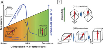
These giant piezoelectric properties arise only under specific conditions. First, as in other solid solution piezoelectric materials, the piezoelectric response depends on composition and is largest near the MPB.Reference Park and Shrout15, Reference Park and Shrout16 This phase boundary separates the rhombohedral (PMN-rich side) and tetragonal symmetry (PT-rich side) in the temperature versus composition phase diagram. For bulk PMN-PT, this phase boundary occurs at 33% PT in the PMN-PT solid solution system.Reference Park and Shrout16 At the MPB, the piezoelectric response of PMN-PT is maximized, as shown in Figure 1a. However, it is not entirely clear how this phase boundary might be modified by strain in a thin film, or from thin-film boundary conditions. As discussed earlier, there are fundamental considerations that indicate different phase diagrams for thin films. There is also some experimental evidence that the mixed-phase region in metal organic chemical vapor deposition PMN-PT thin films grown on SrTiO3 single crystal substrates is different from that of the bulk.Reference Yokoyama, Okamoto, Okamoto, Funakubo, Matsuda, Iijima, Saito, Okino and Yamamoto17 This indicates that the phase diagram can be modified by the presence of the substrate, as well as corresponding epitaxial strain in the film.
(a) Schematic phase diagram of giant piezoelectric relaxor-ferroelectrics. The solid and dotted blue lines represent the longitudinal piezoelectric coefficients in (001) and (111) relaxor-ferroelectric single crystals, respectively. d 33, a longitudinal piezoelectric coefficient, is the mechanical displacement along the applied electric field direction. (b) Schematic illustration of electric-field induced phase transition via polarization rotation from rhombohedral to tetragonal structure as an origin of huge strain level (≈1.7% in bulk single crystals). The red arrow represents the polarization direction. Note: MPB, morphotropic phase boundary. Figures are drawn based on Reference 15.

Second, PMN-PT should be a single crystalline form with (001) orientation rather than polycrystalline. (001) oriented single crystals exhibit large, non-hysteretic piezoelectric coefficients, while (111) oriented ones show a lower and hysteretic piezoelectric response.Reference Park and Shrout15 The unusually large strain levels (≈1.7%) achieved in bulk single crystals originate from the electric-field induced phase transition, as shown in Figure 1b. The applied electric field along [001], not parallel to the [111] direction of spontaneous polarization in rhombohedral PMN-PT, induces a rotation of polarization toward [001]. For PMN-PT with composition in the vicinity of the MPB, such polarization rotation toward [001] easily destabilizes the rhombohedral ground state, resulting in a phase transition to the tetragonal structure. When the tetragonal phase is driven by an electric field from the rhombohedral ground state, additional room for further strain with a longer c/a ratio is provided, increasing the maximum strain level. On the other hand, an electric field applied along the [111] direction, parallel to the polarization, reinforces the original rhombohedral ground state without a structural phase transition, limiting the strain level. Besides this polarization rotation model, several different mechanisms were proposed to explain the giant piezoelectricity near MPB. See Reference 18 and references therein for a detailed discussion.
Third, PMN-PT should be a purely perovskite phase without any second phases. The pyrochlore phase of Pb2Nb2O7 is the most prominent second phase that appears in PMN-PT thin-film synthesis. It can be easily formed due to the comparatively low stability of the perovskite phase.Reference Shrout and Halliyal19 This non-piezoelectric second phase degrades the piezoelectric properties of PMN-PT thin films.
Fourth, the stoichiometry of the five constituent elements of PMN-PT should be exact. In particular, the high volatility of lead oxide (PbO) at the growth temperature leads to off-stoichiometry in films, resulting in not only electrically leaky thin films but also formation of lead-deficient second phases and detrimental grain boundaries. Therefore, in order to achieve giant piezoelectricity in thin films, these four necessary conditions must be met by delicately controlling the thin-film deposition process.
Epitaxial PMN-PT heterostructures on silicon
Integration of high piezoelectric coefficient PMN-PT films on Si substrates has been pursued for more than a decade but was realized only recently due to the complexities discussed previously.Reference Baek, Park, Kim, Aksyuk, Bu, Das, Felker, Lettieri, Vaithyanathan, Bassiri-Gharb, Bharadwaja, Chen, Sun, Jang, Kreft, Nagarajan, Streiffer, Ramesh, Pan, Trolier-McKinstry, Schlom, Rzchowski, Blick and Eom20 The major difficulty in the thin-film synthesis is the extreme sensitivity of film properties to growth parameters. It can be difficult not only to determine optimized growth conditions, but also to reproducibly fabricate high-quality PMN-PT films. Here, we describe recent advances that demonstrate epitaxial integration of PMN-PT with Si, discuss its fabrication into MEMS cantilevers, and discuss broader applications.
Control of growth conditions in high-rate off-axis sputteringReference Das, Kim, Baek, Zavaliche, Yang, Ke, Streiffer, Rzchowski, Ramesh, Pan and Eom21, Reference Baek, Jang, Folkman, Li, Winchester, Zhang, He, Chu, Nelson, Rzchowski, Pan, Ramesh, Chen and Eom22 allows reproducible synthesis of high-quality epitaxial PMN-PT heterostructures on Si using two critical approaches: (1) an epitaxial SrTiO3buffer layer on Si and (2) a miscut Si substrate. The miscut substrate, deliberately cut with a particular angle between the surface normal and [001] crystallographic vectors, has been identified as the key to grow phase-pure PMN-PT films without the lead-deficient pyrochlore phase. The role of substrate miscut likely is to maintain film stoichiometry by decreasing the propensity for volatile species (PbO) to desorb. This vicinal approach has been demonstrated to work well for the growth of epitaxial oxide thin films with volatile species.Reference Das, Kim, Baek, Zavaliche, Yang, Ke, Streiffer, Rzchowski, Ramesh, Pan and Eom21, Reference Bu, Lee, Eom, Tian, Pan, Streiffer and Krajewski23
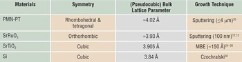
SrTiO3 buffer layers (≈15 nm) on Si were grown by molecular beam epitaxy (MBE).Reference McKee, Walker and Chisholm24–Reference Lettieri26 The epitaxial SrTiO3 buffer layers on Si provide a pseudo-substrate on which other epitaxial perovskite oxide films can grow. Even though the original symmetry of each layer is different in the PMN-PT heterostructure, epitaxy is maintained by the small lattice mismatch of pseudocubic unit cells, as shown in Table I and Figure 2a. As discussed earlier, SrRuO3 can provide an oxide bottom electrode and can also be grown by off-axis sputtering.Reference Eom, Cava, Fleming, Phillips, Vandover, Marshall, Hsu, Krajewski and Peck12, Reference Eom, Sun, Yamamoto, Marshall, Luther, Geballe and Laderman27 SrRuO3 is an ideal bottom electrodeReference Eom, Vandover, Phillips, Werder, Marshall, Chen, Cava, Fleming and Fork13 for epitaxial piezoelectric heterostructures since it is a conductive perovskite with good lattice match with PMN-PT and the SrTiO3template layer. Finally, the PMN-PT films were deposited by high-rate off-axis sputtering.
Material information of each layer in the epitaxial Pb(Mg1/3Nb2/3)O3-PbTiO3(PMN-PT) heterostructure on Si.

MBE, molecular beam epitaxy.
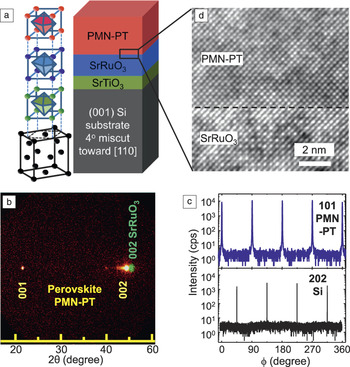
Epitaxial Pb(Mg1/3Nb2/3)O3-PbTiO3 (PMN-PT) (3.5 μm) heterostructure on Si with 4° miscut angle along [110]. (a) Schematic of the PMN-PT heterostructure; (b) x-ray diffraction pattern measured using a two-dimensional area detector of PMN-PT heterostructure on Si; (c) φ-scan of the 101 PMN-PT and 202 Si diffraction peaks. (d) High-resolution cross-sectional transmission electron microscopy image of the PMN-PT and SrRuO3 interface; pseudo-cubic notations are used for both PMN-PT and SrRuO3peak indexing. Note: θ is the angle between the incident x-ray beam and the crystallographic planes; φ is the azimuthal angle of the sample with respect to the vertical axis. Adapted from Reference 20.

Figure 2b shows θ–2θ x-ray diffraction (XRD) scans of 3.5-μm-thick PMN-PT films on 4° miscut Si substrates, where θ is the angle between the incident x-ray beam and the crystallographic planes. It shows excellent epitaxy of (001) perovskite phase with no detectable pyrochlore phase. In contrast, the PMN-PT films on exact Si grown under the same deposition conditions exhibit a large volume of pyrochlore phase with a polycrystalline perovskite phase.Reference Baek, Park, Kim, Aksyuk, Bu, Das, Felker, Lettieri, Vaithyanathan, Bassiri-Gharb, Bharadwaja, Chen, Sun, Jang, Kreft, Nagarajan, Streiffer, Ramesh, Pan, Trolier-McKinstry, Schlom, Rzchowski, Blick and Eom20 This indicates the importance of substrate miscut in controlling film stoichiometry.
Azimuthal φ scans (φ is the azimuthal angle of the sample with respect to the vertical axis) of this phase-pure PMN-PT film in Figure 2c show in-plane epitaxy with a cube-on-cube epitaxial relationship (Figure 2a), [100]pc PMN-PT // [100]pc SrRuO3 // [100] SrTiO3 // [110] Si (“pc” stands for pseudo-cubic). The full width at half maximum (FWHM) of the 002pc ω scan (ω is the rocking angle of the sample) and of the 101pc φ scan are 0.26° and 0.60°, respectively. Commercial PMN-PT bulk single crystals have a FWHM of 0.140 and 0.270, respectively. The high-resolution transmission electron microscopy image (Figure 2d)Reference Baek, Park, Kim, Aksyuk, Bu, Das, Felker, Lettieri, Vaithyanathan, Bassiri-Gharb, Bharadwaja, Chen, Sun, Jang, Kreft, Nagarajan, Streiffer, Ramesh, Pan, Trolier-McKinstry, Schlom, Rzchowski, Blick and Eom20 exhibits an atomically sharp interface between the SrRuO3and PMN-PT layers; the epitaxial match between the layers is clear. Also, chemical composition analysis by wavelength dispersive spectroscopy shows that PMN-PT films are stoichiometric with 0.67 PMN–0.33 PT composition within experimental error. These analyses confirm that PMN-PT thin films on miscut Si satisfy the necessary conditions for giant piezoelectricity shown in the bulk single crystals in terms of stoichiometry, phase-purity, composition, and orientation.
Electrical and piezoelectric properties
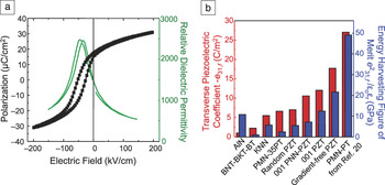
One of the intriguing features of the PMN-PT films is a strong downward built-in bias in the as-grown state. As a result, the polarization versus electric field (P-E) hysteresis loops are shifted (indicating imprint) in the negative direction with a built-in bias of magnitude –38 kV/cm (Figure 3a). This can also be seen in the dielectric permittivity versus electric field measurement. The built-in bias is larger than the coercive field of the PMN-PT films (≈17 kV/cm), resulting in self-poling in the downward direction. This strong imprint benefits the physical properties of PMN-PT films in many ways. First, the built-in bias enhances the magnitude of the remanent polarization (P r): the positive P r is increased from ≈6 μC/cm2 to ≈19 μC/cm2. This in turn increases the piezoelectric response at zero-applied field. Second, the negative built-in bias stabilizes the polarization of PMN-PT in a downward direction. As a result, piezoelectric devices built from these films can be more robust against depolarization due to voltage or temperature excursions, enabling the reliable application of a wider range of the electric field. Note that such a strong imprint cannot be achieved using bulk single crystals. Third, the built-in bias decreases the permittivity at zero field. This increases the figure of merit (same as shown in Figure 3b) for sensors operating in a voltage sensing mode, as well as piezoelectric energy harvesting systems.Reference Muralt4
Electrical and piezoelectric properties of Pb(Mg1/3Nb2/3)O3-PbTiO3 (PMN-PT) thin films on Si. (a) Polarization and relative dielectric permittivity versus electric field measurements on a 1 μm PMN-PT thin film on Si; (b) comparison of figure of merit for piezoelectric actuators (e 31,f) and energy harvesters (e 231,f /εoε33) of PMN-PT film with other reported values. BNT-BKT-BT, KNN, and PNN-PZT stand for Bi0.5Na0.5TiO3-Bi0.5K0.5TiO3-BaTiO3, K0.5Na0.5NbO3, and 0.3Pb(Ni0.33Nb0.67)O3-0.7Pb(Zr0.45Ti0.55)O3, respectively. e 31,f, εo, and εrstand for the effective transverse piezoelectric coefficient, dielectric permittivity in vacuum, and relative dielectric permittivity, respectively. PMN-PT thin films on Si exhibit unparalleled piezoelectric and energy harvesting figures of merit. Adapted from Reference 20.

As discussed previously, this strong imprint is beneficial to applications of PMN-PT thin films. There could be several origins of this relatively strong imprint. Defect dipoles, trapped carriers, strain gradients, nonswitching domains, and structural asymmetries have all been suggested to lead to imprint.Reference Grossmann, Lohse, Bolten, Boettger, Schneller and Waser28, Reference Warren, Pike, Vanheusden, Dimos, Tuttle and Robertson29 In the PMN-PT films, comparison of interdigitated, top-surface only electrodes with an asymmetric top and bottom electrode configuration suggests that in these films, the imprint arises at least in part from the asymmetric interfaces between Pt/PMN-PT and PMN-PT/SrRuO3, although further investigations are needed to identify the exact mechanism.Reference Baek, Park, Kim, Aksyuk, Bu, Das, Felker, Lettieri, Vaithyanathan, Bassiri-Gharb, Bharadwaja, Chen, Sun, Jang, Kreft, Nagarajan, Streiffer, Ramesh, Pan, Trolier-McKinstry, Schlom, Rzchowski, Blick and Eom20
The transverse piezoelectric coefficient, e 31,f, provides the figure of merit for the majority of micromachined piezoelectric sensors and actuators. PMN-PT films on Si show a maximum e 31,f value of –27 C/m2 ± 3 C/m2 measured by wafer flexure,Reference Shepard, Moses and Trolier-McKinstry30 the highest reported for any piezoelectric thin film. (Uncertainties quoted throughout the article have statistical uncertainties of one standard deviation.) This directly reduces the required driving voltage for piezoelectric MEMS actuators.
Moreover, due to the combination of a large piezoelectric response and low dielectric permittivity by imprint, the figure of merit for MEMS piezoelectric energy harvesting,Reference Roundy31–Reference Dubois and Muralt36 ${{e_{31,f}^2 } \over {{\rm{\varepsilon }}0{\rm{\varepsilon }}_{33} }}$, (ε33: relative dielectric permittivity, ε0: dielectric permittivity in vacuum) shows the highest value. This is also indicative of an enhanced figure of merit for the voltage-driven sensors. Figure 3bReference Baek, Park, Kim, Aksyuk, Bu, Das, Felker, Lettieri, Vaithyanathan, Bassiri-Gharb, Bharadwaja, Chen, Sun, Jang, Kreft, Nagarajan, Streiffer, Ramesh, Pan, Trolier-McKinstry, Schlom, Rzchowski, Blick and Eom20 compares the figure of merit for the PMN-PT film with that for PZT and other piezoelectric materials, demonstrating their advantages for energy-harvesting applications as well as piezoelectric MEMS. These improved responses for actuating and energy-harvesting in PMN-PT films are also confirmed by comparative simulations of PMN-PT and PZT cantilevers using self-consistent data,Reference Nguyen, Vu, Blank and Rijnders9 confirming that the figure of merit is a good indicator of device performance.
The combination of high piezoelectric response with the ability to drive the materials hard without depolarization will enable better resolution and deeper penetration depth in film-based ultrasound imaging.Reference Kim, Kim, Griggio, Tutwiler, Jackson, Trolier-McKinstry and Choi37 Furthermore, the ability to achieve large displacements in small structures with high resonant frequencies offers the possibility for faster switching networks for low-power CMOS circuits,Reference Akarvardar, Eggimann, Tsamados, Chauhan, Wan, Lonescu, Howe and Wong38 lower voltage fully mechanical logic devices.Reference Tsai, Kuo, Lin and Chen39, Reference Blick, Qin, Kim and Marsland40 Moreover, the integration of multifunctional materials in an epitaxial structure with giant piezoelectricity opens up a new field of dynamically strain-controlled devices,Reference Biegalski, Dorr, Kim and Christen41, Reference Pellegrino, Biasotti, Bellingeri, Bernini, Siri and Marre42 which enables controlling optical, electrical, and magnetic properties through induced stain.
PMN-PT microcantilevers
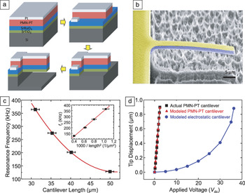
The development of microfabrication processes that do not degrade the large piezoelectric coefficients of PMN-PT thin films is essential for technological applications of these devices. Cantilevers are often fabricated as prototypical structures for electromechanical devices utilizing the e 31 coefficient, such as actuators and energy harvesters. Figure 4 a shows a successful fabrication process, preserving the high piezoelectric properties of PMN-PT films.Reference Baek, Park, Kim, Aksyuk, Bu, Das, Felker, Lettieri, Vaithyanathan, Bassiri-Gharb, Bharadwaja, Chen, Sun, Jang, Kreft, Nagarajan, Streiffer, Ramesh, Pan, Trolier-McKinstry, Schlom, Rzchowski, Blick and Eom20
Fabrication and characterization of Pb(Mg1/3Nb2/3)O3-PbTiO3 (PMN-PT) microcantilevers. (a) Microfabrication process for PMN-PT cantilevers. Ar+ ion milling was used to etch the Pt/PMN-PT layer, exposing the bottom electrode. Additional ion milling was performed to etch Pt/PMN-PT/SrRuO3/SrTiO3/Si, defining the cantilevers. Then, inductively coupled plasma etching was used to selectively etch Si, releasing PMN-PT cantilevers from the Si substrate. The cantilevers consist of Pt (60 nm)/PMN-PT (270 nm)/SrRuO3 (100 nm)/SrTiO3 (13 nm); (b) scanning electron microscopy image of a PMN-PT cantilever. Yellow and blue are colored to distinguish the Pt top electrode and PMN-PT heterostructure, respectively; (c) resonance frequency versus cantilever length measurement. The inset is resonance frequency versus 1/length2; (d) tip displacement of 34-μm-long PMN-PT cantilever versus applied dc voltage measurement. All measurements were performed at room temperature and ambient pressure. Error bars represent one standard deviation and are not shown where statistical uncertainties are smaller than the symbol size. PMN-PT microcantilevers fabricated from PMN-PT thin films on Si preserve piezoelectric properties that rival those of the bulk single crystal PMN-PT. Note: f 0, resonance frequency. Adapted from Reference 20.

Depth-controlled Ar+ ion milling with a liquid nitrogen-cooling stage was used to etch metal and oxide layers to define the cantilever structure. An inductively coupled plasma with a 1:1 mixture of SF6 and O2 gases was used to etch the Si substrate beneath the PMN-PT heterostructures, where the plasma etches Si from the exposed silicon side walls, releasing the PMN-PT cantilevers. No significant etching of other layers during the Si undercut was found.Reference Baek, Park, Kim, Aksyuk, Bu, Das, Felker, Lettieri, Vaithyanathan, Bassiri-Gharb, Bharadwaja, Chen, Sun, Jang, Kreft, Nagarajan, Streiffer, Ramesh, Pan, Trolier-McKinstry, Schlom, Rzchowski, Blick and Eom20 The resulting PMN-PT microcantilever is shown in Figure 4b. Various length cantilevers can be fabricated in this way to evaluate the effect of processing on the piezoelectric layer and to determine in-place piezoelectric characteristics of the thin-film layer.
These characteristics are most commonly determined from the overall mechanical response of the cantilever, measured by white light interferometry,Reference Wyant43 which maps out displacements over the entire surface of the cantilever. This method can determine both dc response, where the cantilever profile as a function of dc bias voltage is determined, as well as ac response, where the cantilever resonant frequency is determined by scanning the frequency of an ac bias. For ac measurements, strobed white light interferometry can be used.
In the case of the PMN-PT cantilevers, a sine wave of 50 mV peak to peak was applied without dc bias, and the frequency was changed until the resonance was found. The resonance frequency was independent of voltage amplitude for voltages below 50 mV. The statistical measurement uncertainty is less than ±0.5 kHz, limited by the mechanical quality factor of the cantilever resonance in ambient air, with the typical FWHM peak width of 4 kHz. Figure 4c shows resonance frequency as a function of cantilever length. It scales well as 1/length2as expected from simple mechanical models, indicating that PMN-PT films are spatially homogeneous in terms of thickness and composition over distances from a few micrometers to the inter-cantilever distance of a few hundred micrometers.
Figure 4d shows the mechanical response of a 34-μm-long cantilever as a function of the applied dc voltage. The tip of the cantilever moves linearly with voltage with a sensitivity of 0.375 μm/V ± 0.005 μm/V. This cantilever motion is consistent with the finite element simulation that used the material parameters reported for bulk single crystal PMN-0.33PT.Reference Zhang, Jiang and Cao44 This indicates that the PMN-PT films on Si still exhibit comparable physical properties to bulk single crystal unaffected by the fabrication processes.
These results also demonstrate that active MEMS incorporating piezoelectric layers with giant piezoelectric response are viable competitors to electrostatic actuation.Reference Uchino1–Reference Muralt, Polcawich and Trolier-McKinstry5 Major drawbacks of electrostatic actuation are the required high control voltage and the nonlinear response. The former often prevents scaling down and denser integration of the electronic drivers for actuator arrays. The latter hampers precise control of positioning and limits the range of operating voltage. The PMN-PT cantilever substantially lowers this driving voltage and exhibits linear displacement with voltage compared to the electrostatic cantilever simulated with comparable structure in Figure 4d. Note that the electromechanical performance of PMN-PT cantilevers is expected to be further enhanced with optimized and precisely controlled thicknesses of all layers for required stiffness and displacement,Reference Muralt, Ledermann, Baborowski, Barzegar, Gentil, Belgacem, Petitgrand, Bosseboeuf and Setter45 for instance using silicon on insulator wafers.
MEMS applications of epitaxial PMN-PT thin films
It is particularly interesting to consider the potential impact of this technology on applications requiring dense integration of many MEMS actuated devices to provide novel system functionality. When scaling to hundreds or thousands of elements, it is essential that these mechanical systems can be controlled by low voltage signals that can be provided by small, cheap, densely integrated analog or digital circuits. This is particularly important when the density is such that the electronics have to be integrated in a monolithic or hybrid manner directly above or below the MEMS, as in some optical micromirror array applications,Reference Watson, Aksyuk, Simon, Tennant, Cirelli, Mansfield, Pardo, Lopez, Bolle, Papazjan, Basacanhally, Lee, Fullowan, Klemens, Miner, Kornblit, Sorsch, Fetter, Peabody, Bower, Weiner and Low46 as well as potential future applications of MEMS-tunable nanophotonics.Reference Basavanhally, Lopez, Aksyuk, Ramsey, Bower, Cirelli, Ferry, Frahm, Gates, Klemens, Lai, Low, Mansfield, Pai, Papazian, Pardo, Sorsch and Watson47–Reference Miao, Srinivasan, Rakher, Davanco and Aksyuk49 At the same time, it is desirable, and in some cases essential, to increase the speed of these mechanical elements, which is accomplished by scaling down their size. This scaling to lower drive voltages, smaller elements, and higher speeds often cannot come at the expense of decreased actuator range, which is set by some external parameter (e.g., the wavelength of light in an optical application). This results in a challenging set of system constraints. Integration of high energy density piezoelectric actuators may help overcome this challenge. In addition to increased electromechanical coupling, the lower dielectric constant will decrease the capacitive load and typically lower the power dissipation in the drive circuit for high frequency actuation. Finally, better quality single crystal piezoelectric films may lower intrinsic material losses, improving performance of resonant transducers and decreasing thermal mechanical noise in MEMS sensors.
Conclusions
Active microelectromechanical systems (MEMS) incorporating piezoelectric thin films as the central element can be reliably fabricated, but even the highest performance traditional piezoelectric materials constrain potential applications. Recent breakthroughs in synthesizing high-quality epitaxial Pb(Mg1/3Nb2/3)O3-PbTiO3(PMN-PT) films on Si have provided new opportunities to build MEMS devices with dramatically higher performance and to extend piezoelectric actuators to the nanoscale. Integrating giant piezoelectric active materials could generate the required large linear forces at small drive voltages with fast actuation, provide accurate displacements at high integration densities, reduce the voltage burden on the integrated control electronics, and decrease nanoelectromechanical system complexity. These heterostructures have tremendous potential to develop necessary actuators, are compatible with silicon nanofabrication processes, and can be integrated with silicon-based electronics. The strong piezoelectric activity of these PMN-PT thin films promises dramatically greater design freedom for realization of smaller electromechanical devices with even better performance, enabling device applications such as ultrasound medical imaging, micro-fluidic control, energy harvesting, and piezotronics.
However, there remain unanswered questions about this new platform: how can the piezoelectric response of PMN-PT thin films be optimized? How can we design PMN-PT film composition, thickness, strain state, and substrate clamping to produce the optimum device performance for a given device geometry?
These require an understanding of the fundamental physics in this system. For example, the interplay between strain, substrate clamping, defects, and possible shift of morphotropic phase boundary composition needs to be understood. For this, a wide range of interdisciplinary works would be desirable from materials science, to physics, to mechanics, and to computational science. Successful integration of giant piezoelectric materials on Si provides a new challenge and will stimulate fruitful, collaborative research opportunities in solid-state physics as well as technology.
Acknowledgments
The authors acknowledge support from the National Science Foundation grant number ECCS-0708759.