I. INTRODUCTION
With the increasing demand of digital voice, high-definition video, and other big-data services, wireless communication system requires wider operation bandwidth. Wideband bandpass filter (BPF), with fractional bandwidth (FBW) over 20% and as a significant component in wideband communication system, has been studied extensively [Reference Shi, Feng, Che and Xue1].
Several technologies have been developed to design wideband BPFs. Multi-mode resonator is a frequently-used method of designing wideband filter, which is realized by utilizing a plurality of resonant modes in a composite resonator. Therefore, many compact and wideband microstrip BPFs have been developed using multi-mode resonator [Reference Nosrati and Mirzaee2–Reference Zhu, Sun and Menzel4]. In microwave and millimeter-wave applications, the broadside coupling between resonators can be used easily to achieve wideband filter, such as wideband BPFs using broadside coupling in multilayers liquid crystal polymer technology have been reported [Reference Shen, Shao, You and Ban5–Reference Shen, Wang, You and Shao7], and the tight coupling between coplanar waveguides or slot-line structures also can be used to design wideband BPFs [Reference Thomson and Hong8–Reference Dong, He, Yang and Ma9]. Some wideband BPFs using mixed electromagnetic (EM) coupling also have been reported in [Reference Qian, Boria, Hong and Meyer10, Reference Xu11], most of which are with good frequency selectivity. In addition, low- and high-pass filters series together can realize wideband BPFs. For example, the bandpass characteristic of substrate integrated waveguide-to-defected ground structure (SIW–DGS) cell is the high- and low-pass type, which is a combination of the inherent high-pass characteristic of SIW and the bandgap function of DGS [Reference Huang, Shao and Liu12–Reference He, Cai, Shao, Li and Huang14].
In this work, an improved wideband filter using multi-mode resonator and mixed EM coupling is designed, fabricated and measured. To increase the bandwidth, two quarter-wavelength stepped impedance resonators (SIRs) and a multi-mode resonator with four short stubs are used in the filter. The coupling between multi-mode resonator and quarter-wavelength SIR is mixed EM coupling. The electrical coupling is achieved by the gap between open-circuited ends of the stubs, and the magnetic coupling is generated by a high-impedance transmission line between the two resonators. Compared with the BPFs using dual-behavior resonators in [Reference Feng and Che15–Reference Manchec, Quendo, Favennec and Eric Rius18], the proposed filter in this work provides wider bandwidth with smaller circuit size. Accordingly, the wideband filter with good selectivity can be used in a microwave/millimeter-wave high-precision imaging system or high-speed communication system.
II. THEORETICAL ANALYSIS AND DESIGN
A) Dual-mode resonator with shorted stubs
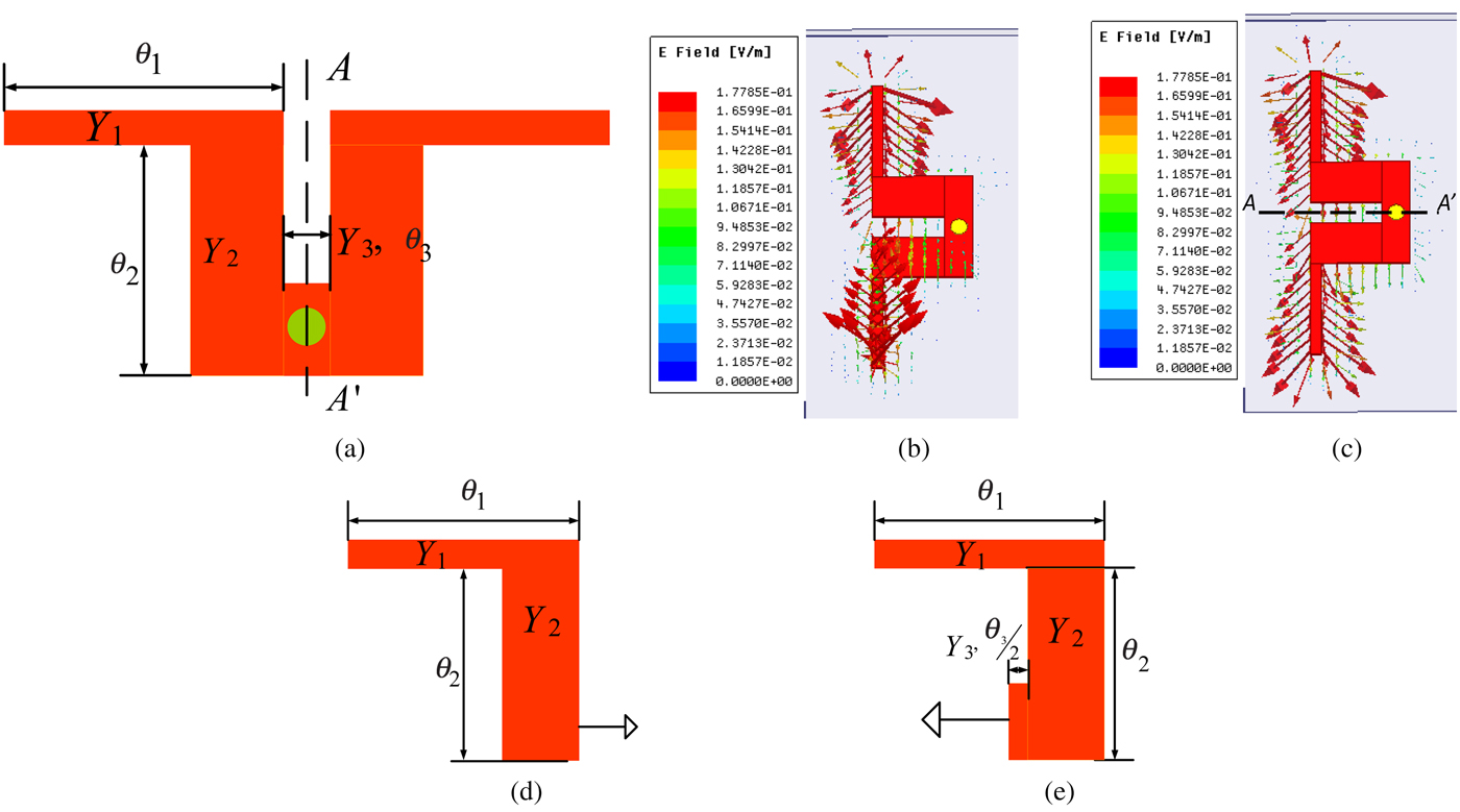
Figure 1(a) shows the dual-mode resonator, which consists of two stubs and a center-shorted microstrip transmission line. Since the resonator is symmetrical by plane A–A ′, it can be analyzed by the odd- and even-mode equivalent circuit methods. Figures 1(b) and 1(c) show the E-field at odd-mode and even-mode frequency, respectively, it is known that the E-field in the center-shorted microstrip transmission line is weaken, and the E-field at even-mode resonant frequency in Fig. 1(c) is symmetrical by plane A–A ′.
Dual-mode resonator: (a) basic structure, (b) E-field at odd-mode frequency, (c) E-field at even-mode frequency, (c) odd-mode, and (d) even-mode equivalent circuits.

Accordingly, for the odd-mode excitation, the odd-mode equivalent circuit can be shown as Fig. 1(d), and the input admittance Y inodd can be given by
 $$Y_{in_{odd}} = Y_1 \displaystyle{{{Y_2} - {Y_1} \tan \theta_1 \tan \theta_2 } \over {{j(Y}_1 \tan \theta_2 + Y_2 \tan \theta_1 )}}.$$
For the even-mode excitation, the even-mode equivalent circuit can be shown as Fig. 1(e). To simplify the analysis, Y 2 = Y 3 is assumed, then the input admittance Y ineven can be given by
 $$ Y_{in_{even}} = Y_1 \displaystyle{{ {Y_2} - {Y_1} \tan \theta _1 \tan ( \theta _2 + \theta _3 /2)} \over { {j(Y}_1 \tan ( \theta _2 + \theta _3 /2) + Y_2 \tan \theta _1 )}}.$$
According to the resonant condition of Y in = 0, the resonant condition of odd- and even-modes can be calculated from (1) and (2)
 $$\tan \theta _1 \tan \theta _2 = \displaystyle{{ Y_2 } \over { Y_1 }},$$
 $$\tan \theta _1 \tan ( \theta _2 + \displaystyle{{ \theta _3 } \over 2}) = \displaystyle{{ Y_2 } \over { Y_1 }}.$$
From (3) and (4), it can be obtained that the places of input and output port have no relationship with the resonant modes. When the substrate and ratio of Y 2 /Y 1 are given, the odd-mode frequency is only decided by the length of stubs (θ 1 and θ 2), and the even-mode frequency is decided by the length of stubs (θ 1 and θ 2) and the length of shorted microstrip line (θ 3). By adjusting the length of the stubs and center-shorted microstrip line, the resonant modes of multi-mode resonator can be changed.
B) Mixed EM coupling
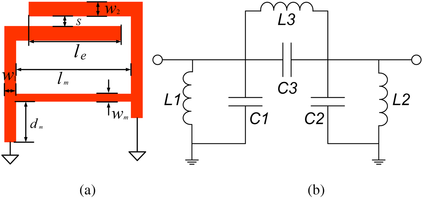
The coupling structure between quarter-wavelength SIR and multi-mode resonator is shown in Fig. 2(a), including electric and magnetic coupling. The electric coupling is realized by the gap between the open-circuited end of two resonators, and the magnetic coupling is implemented by a high-impedance transmission line, which connects the two resonators together and acts as a coupling inductance. The equivalent circuit of the structure is shown in Fig. 2(b), the equivalent shunt inductances (L 1 and L 2) are realized by the short end and L 3 is the inductance of high-impedance transmission line, the equivalent shunt capacitances (C 1 and C 2) are realized between the SIR and the ground, the coupling capacitance (C 3) is achieved by the gap between the two open ends.
(a) Structure of mixed EM coupling, (b) equivalent circuit of mixed EM coupling.

According to (5), which demonstrates the relationship between coupling coefficient K and physical dimensions, the design curves can be extracted by an EM simulator.
 $$k = \displaystyle{{f_2^2 - f_1^2 } \over {f_2^2 + f_1^2 }},$$
where f 1 and f 2 are the lower and upper resonant modes.
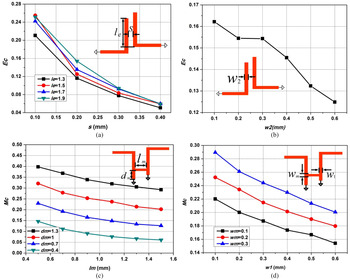
To extract the coupling coefficient, the structures of mixed EM coupling are simplified. As shown in Fig. 3, the electric coupling coefficient E c can be extracted by modeling the slot(s), length (l e ), and width (w 2) of coupling strip. The magnetic coupling coefficient M c can be extracted by modeling the length (l m ) and width (w m ) of transmission line, and the width of short end (w 1) and its distance to the ground (d m ). Figure 3(a) shows the extracted values of E c versus l e and s, which depicts E c decreases with s and increases with l e . Figure 3(b) shows the extracted values of E c versus w 2, which depicts E c decreases with w 2. Figure 3(c) shows the extracted values of M c versus l m and d m , which depicts M c decreases with l m and increases with d m . Figure 3(d) shows the extracted values of M c versus w m and w 1, which depicts M c decreases with w 1 and increases with w m .
(a) Electric coupling coefficient E c versus l e and s, (b) electric coupling coefficient E c versus w 2, (c) magnetic coupling coefficient M c versus l m and d m , (d) magnetic coupling coefficient M c versus w m and w 1.

C) Initial filter with dual-mode resonator and mixed EM coupling
Based on the aforementioned dual-mode resonator and mixed EM coupling structure, a novel filter can be designed. For the demonstration, the initial filter is designed with the given specifications: the center frequency is 17 GHz and bandwidth is 3.5 GHz (FBW = 20%), the in-band return loss is larger than 20 dB, and the frequency of transmission zero is 14 GHz. According to the specifications, the mixed coupling coefficient K is calculated to be: K = 0.14. The mixed coupling coefficient K and transmission zero f m are related with electric- and magnetic-coupling coefficient, the relationship is as follows: [Reference Chu and Wang19]
 $$k = \displaystyle{{w_{odd}^2 - w_{even}^2 } \over {w_{odd}^2 + w_{even}^2 }} = \displaystyle{{M_c - E_c} \over {1 - E_cM_c}},$$
 $$f_m = f_r \times \sqrt {{\textstyle{{E_c} \over {M_c}}}} ,$$
where w even and w odd are the frequencies of the even and odd modes, respectively; E c and M c are the electric and magnetic coupling coefficients, respectively; f r is the resonant frequency of the resonator. Equation (5) shows the relationship between mixed coupling coefficient K and E c and M c , and Equation (6) shows the relationship between transmission zero f m and E c , and M c .
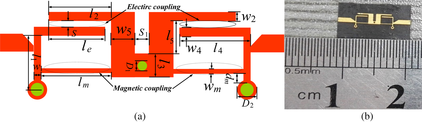
Considering f m = 14 GHz and K = 0.14, the electric coupling coefficient E c and magnetic coupling coefficient M c can be calculated to be M c = 0.39 and E c = 0.264 from (5) and (6). By comparing the calculated E c = 0.264 with the curve in Figs 3(a) and 3(b), the initial dimension of s, l e , and w 2 can be determined, for example, when setting w 2 = 0.2, then l e and s can be determined as s = 0.1 and l e = 1.9. In addition, the initial dimensions of w m , w 1, l m , and d m can be determined as w m = 0.1, w 1 = 0.3, l m = 1.3, and d m = 1.08 when compare M c = 0.39 with the curve in Figs 3(c) and 3(d); and the initial dimensions of the multi-mode resonator (s 1, l 2, w 2, l 5, w 5, l 3) can be determined by the above odd- and even-mode analyses. Above all, it can be seen that the initial dimensions of the filter can be obtained by theory analysis. However, there are many parasitic coupling in the filter, such as the coupling between the end of line l e and the corner of the second line. The theory analysis only can provide initial dimensions for the physical realization. The final dimensions still need to be optimizing by a three-dimensional (3D) full-wave finite-element method simulator. The structure of the initial filter is shown in Fig. 4(a), and the final dimensions in the figure are given as: l 1 = 1.72, w 1 = 0.13, l 2 = 2.6, w 2 = 0.2, l e = 1.7, l 3 = 0.5, l 4 = 1.93, w 4 = 0.16, l 5 = 1.1, w 5 = 0.8, l m = 1.9, w m = 0.1, s 1 = 0.4, s = 0.21, d m = 0.42, D 1 = 0.15, D 2 = 0.25 (unit: mm).
(a) Structure of initial filter; (b) Photograph of the fabricated filter.

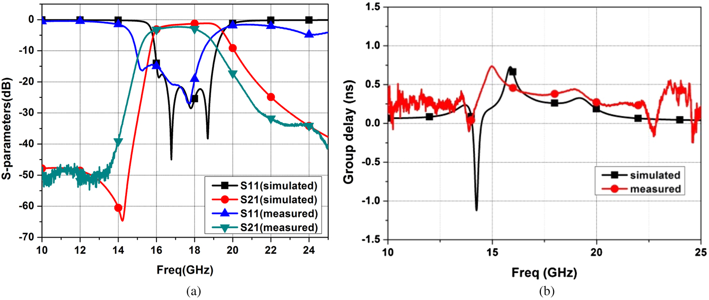
The initial filter is designed and fabricated on Rogers RT/duroid 5880 substrate, which is with a relative permittivity of 2.2 and a loss tangent of 0.0009. And thickness of the substrate is 0.254 mm. The fabricated BPF is shown in Fig. 4(b), its effective circuit size is 7.66 × 2.54 mm2 (0.118 λg 2, λg is the guide wavelength at 17 GHz). It is noted the proposed filter has a relatively compact size. The wideband BPF is measured by the Agilent Vector Network Analyzer N5245A, and the simulated and measured results are shown in Fig. 5.
Simulated and measured results of the initial filter: (a) S-parameters, (b) group delay.

Figure 5(a) shows the simulated and measured 3 dB bandwidths are 3.6 and 3.22 GHz, respectively. The simulated and measured insertion loss are 1.5 and 2.3 dB (the insertion loss of SMA connectors and adapters is about 0.5 dB based on an additional measurement), respectively. Figure 5(b) shows the simulated and measured group delays are 0.27 and 0.37 ns at central frequency, and the variations are within 0.46 and 0.36 ns over the whole passband. The differences between the simulated and measured results are caused by the inevitable error in relative permittivity variation, fabricating and measuring.
III. IMPROVED FILTER WITH ENHANCED BANDWIDTH
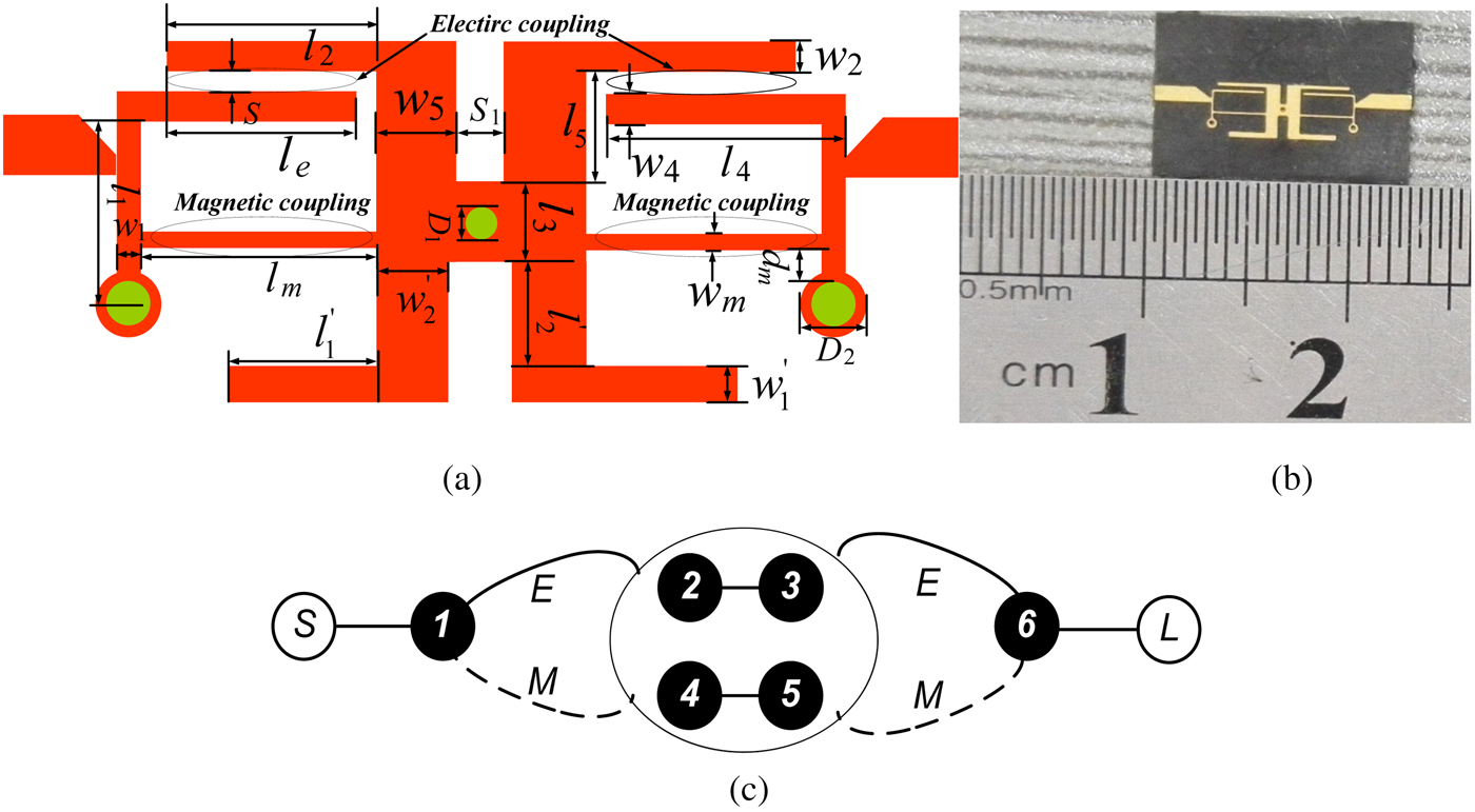
According to the above analysis of dual-mode resonator with two stubs, only two resonant modes in the resonator, the odd mode produces a pole and the even mode produces a pole. The measured FBW of the initial filter is only 18.9%, as shown in Fig. 5(a). To further increase the bandwidth, two other stubs are extended downwardly in the resonator, to add two additional poles, as shown in Fig. 6(a). The coupling between the quarter-wavelength resonators and multi-mode resonator are mixed EM coupling, as shown in Fig. 6(c). From the above odd- and even-mode analyses, the resonance can be separately adjusted by the length of microstrip line.
(a) Structure of the improved BPF; (b) Photograph of the fabricated BPF; (c) The coupling diagram of the improved filter.

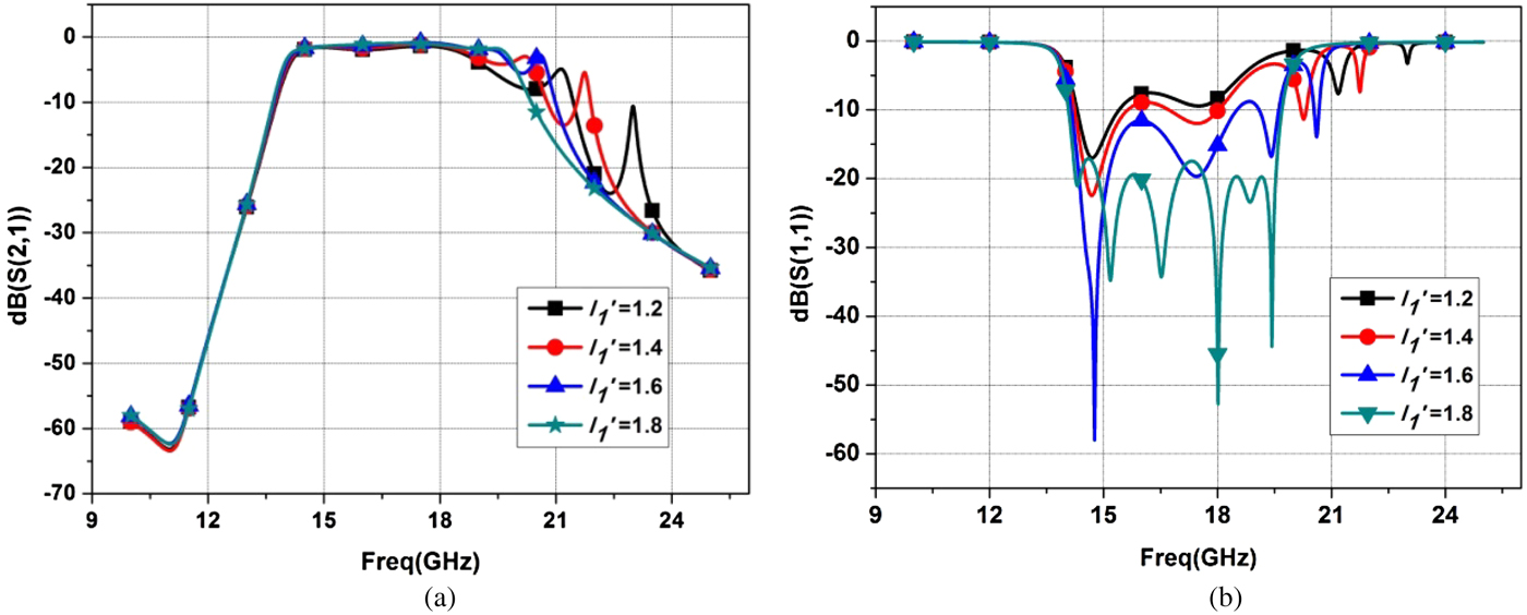
Figure 7 shows the simulated performances of the improved BPF with different values of l 1 ′, it shows the two higher resonances can be obviously adjusted by the length of microstrip line, the shorter the length, the higher the resonance, which conforms the odd- and even-mode analysis results.
Simulated S-parameter of the improved BPF with varied l 1 ′: (a) S 21, (b) S 11.

In the filter, the specifications are given as: the central frequency is 17 GHz and bandwidth is 6 GHz (FBW = 35.3%), the in-band return loss is < 20 dB, and the frequency of transmission zero is 11 GHz, which is considered for a wideband wireless communication system. According to the specifications, the mixed coupling coefficient is calculated to be K = 0.217, then the electric coupling coefficient E c and magnetic coupling coefficient M c can be extracted to be E c = 0.149 and M c = 0.354 from (5) and (6). Compared with the curve in Fig. 3, the initial dimensions of the mixed EM coupling structure can be determined, and the initial dimensions of the multi-mode resonator can be determined by odd- and even-mode analyses. The final structure can be optimized by 3D EM simulator, and the dimensions in Fig. 6(a) are given as: l 1 = 1.56, w 1 = 0.1, l 2 = 3.12, w 2 = 0.18, l e = 2.32, l 3 = 0.59, l 4 = 2.58, w 4 = 0.12, l 5 = 0.79, w 5 = 0.7, l m = 2.58, w m = 0.1, s 1 = 0.29, s = 0.18, l 1 ′ = 1.8, w 1 ′ = 0.28, l 2 ′ = 0.86, w 2 ′ = 0.59, d m = 0.35, D 1 = 0.15, D 2 = 0.25(unit: mm).
The improved wideband filter is fabricated by the same substrate, and the photograph of the fabricated BPF is shown in Fig. 6(b). The effective dimension of the filter is 8.65 × 2.7 mm2 (0.126 λg 2, where λg is the guide wavelength at the central frequency), which is almost the same size as the initial filter.
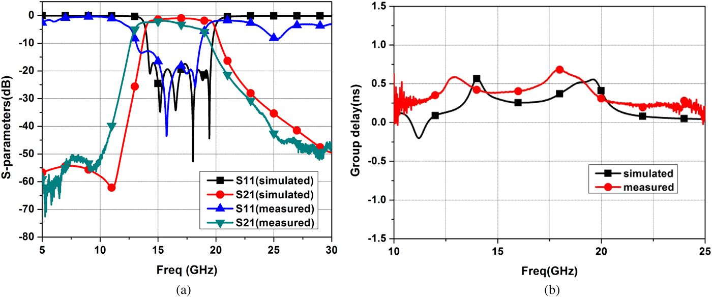
Figure 8(a) shows the S-parameters, it depicts the measured insertion loss in the center frequency of 15.86 GHz is 2 dB, and the 3 dB bandwidth is 5.72 GHz (FBW is about 36%). The flatness in the passband is not very good. This is because the substrate is easily deformed in the processing, which changes the two additional stubs, so that the insertion loss in the upper passband is larger. Figure 8(b) shows the group delay, it depicts the measured group delay at central frequency is 0.4 ns and the variation is within 0.28 ns over the passband, which demonstrates that the filter has a good linear response. The discrepancy between simulated and measured group delay is mainly caused by the variation of relative dielectric constant, which also makes the resonance frequencies move to the left. Compared with the results of initial filter in Fig. 5, we can find that the improved filter has wider bandwidth and smaller insertion loss. This is because the two additional stubs disturb the two resonant modes and add two resonance frequencies in the improved filter.
Simulated and measured results of the improved filter: (a) S-parameters, (b) group delay.

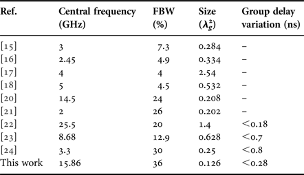
The comparison with some reported similar BPFs is presented in Table 1 [Reference Feng and Che15–Reference Manchec, Quendo, Favennec and Eric Rius18, Reference Zhu, Zhang and Yu20–Reference Wong, Feng, Zhu and Chu24]. It shows the improved filter achieves wider bandwidth and smaller size than BPFs using dual-behavior resonators in [Reference Feng and Che15–Reference Manchec, Quendo, Favennec and Eric Rius18] and multi-mode BPFs in [Reference Zhu, Zhang and Yu20–Reference Wong, Feng, Zhu and Chu24]. In addition, it also has better linear response than some multi-mode BPFs in [Reference Cai, Ma, Guan, Zheng, Tetsuo and Gen22–Reference Wong, Feng, Zhu and Chu24].
Comparison with some reported similar bandpass filters.

IV. CONCLUSION
A wideband BPF based on multi-mode resonator and mixed EM coupling is proposed in this paper. The multi-mode resonator is composed of multiple short stubs, which introduces more resonances but not increases the size. The mixed EM coupling is used between the quarter-wavelength SIR and the multi-mode resonator, which produces transmission zero in the lower stopband. As a result, the proposed filter achieves wide bandwidth, compact size, and good selectivity, so that it can be used for the high-precision imaging system or wideband wireless communication applications.
ACKNOWLEDGEMENTS
This work was supported in part by NSFC (grant numbers 61571084 and 61561021), in part by NCET (grant number NCET-13-0095), in part by the FRF for CU (grant number ZYGX2014J016), and in part by the SRF for ROCS, SEM.
 Mengkui Shen was born in Xianning, China, in 1988. He received the B.Sc. degree from the China Three Gorges University, Yichang, China, in 2011, and the M.Sc. degree from the University of Electronic Science and Technology of China, Chengdu, China, in 2014. He is currently working toward the Ph.D. degree at the University of Electronic Science and Technology of China. His current research interests include microwave and millimeter-wave circuits and systems.
 Xian Qi Lin (M'08–SM'15) was born in Zhejiang, China, in 1980. He received the B.S. degree in Electronics Engineering from the University of Electronic Science and Technology of China (UESTC), Chengdu, China, in 2003, and the Ph.D. degree in Electromagnetic and Microwave Technology from Southeast University, Nanjing, China, in 2008. He joined the Department of Microwave Engineering, UESTC, in 2008, and was an Associate Professor from 2009 to 2015. From 2011 to 2012, he was a Post-Doctoral Researcher with the Department of Electromagnetic Engineering, Royal Institute of Technology, Stockholm, Sweden. He is currently a Full Professor at UESTC. He has authored more than ten patents, more than 40 scientific journal papers, and 20 conference papers. His research interests include microwave/millimeter-wave circuits, metamaterials, and antennas.
 Zhaosheng He was born in HongAn, HuBei, China, in 1986. He is currently working toward the Ph.D. degree at the University of Electronic Science and Technology of China (UESTC), Chengdu, China. His current research interests include microwave and millimeter-wave planar circuits, components, and wireless communication & radar systems.