I. INTRODUCTION
The electrical or light-emitting properties of semiconductors, which are essentially decided by their electronic structures, could be modified through forming various nanostructures and further tailored by constructing multiform nanoheterostructures.Reference Rohrmoser, Baldauf, Harley, Lagoudakis, Sapra and Eychmuller1–Reference Willander, Nur, Bano and Sultana10 For example, it has been demonstrated that either multi-band emissions or stable and efficient photo/electro-luminescence could be realized through forming various nanoheterostructures such as InGaN/CdS,Reference Rohrmoser, Baldauf, Harley, Lagoudakis, Sapra and Eychmuller1 Ge/Si,Reference Xiang, Lu, Hu, Wu, Yan and Lieber2, Reference Rauter, Fromherz, Vinh, Murdin, Mussler, Grutzmacher and Bauer3 ZnO/NiO,Reference Long, Fang, Huang, Mo, Xia, Dong, Meng and Zhao4 carbon nanotube (CNT)/Si,Reference Tzolov, Chang, Yin, Straus, Xu and Brown5 GaAs/AlxGa1−xAs,Reference Yi, Narayanamurti, Lu, Scarpulla and Gossard6 ZnO/GaN,Reference Jeong, Oh, Ham, Lee and Myoung7 CdS/ZnO,Reference Tak, Hong, Lee and Yong8 and ZnO/Si.Reference Hsieh, Chen, Lin, Shiu, Hofmann, Chern, Jia, Yang, Chang, Huang, Tseng, Chen, Chen, Lin, Liang and Chen9–Reference Chang, Jian, Lee, Lin and Juang11 Technically, the nanoheterostructures were usually prepared by growing one kind of semiconductor material onto the other, with the latter being pretreated to form some kinds of nanostructures and acting as both a compositional material and a well-established nanotemplate.Reference Hsieh, Chen, Lin, Shiu, Hofmann, Chern, Jia, Yang, Chang, Huang, Tseng, Chen, Chen, Lin, Liang and Chen9–Reference Chang, Jian, Lee, Lin and Juang11 Considering that the technology based on crystalline Si has been developed many years ago and always got much attention, the exploration of Si-based nanoheterostructures might be of key importance in developing future optoelectronic nanodevices, such as Si-based optoelectronic nanodevices or Si ultralarge-scale integrated circuits with electric-optics to overcome the speed limitation of electrical interconnects and to `add extra functionalities on Si chips.
In an earlier published article, a novel silicon hierarchical structure, here, the nanoporous silicon pillar array (NSPA), was prepared and characterized by our group.Reference Xu and Li12 It has been proved that NSPA could be well-characterized by a regular array of micron-sized, quasi-identical and highly porous Si pillars, with the pore walls constructed by SiO2-encapsulated Si nanocrystallites.Reference Xu and Li12 Furthermore, the observation of strong and stable red photoluminescence (PL) at room temperature indicates that NSPA might be a well-established substrate for assembling Si-based functional nanoheterostructures. Based on NSPA, large area regular pillar array of CdS/Si nanoheterostructure with strong three primary color PL and electrical rectification phenomenon was obtained, which indicated that NSPA might be a potential template for developing various Si-based nanoheterostructures with enhanced physical properties.Reference Xu and Li13, Reference Xu and Li14 For example, if the strong red emission of NSPA could be combined with a blue/green emission by modification of the NSPA surface, it would be possible to obtain white light. This would provide a cheap route to Si-based white light-emitting diodes, which is important for the display or light-source applications. Recently, ZnO as a most promising semiconductor has arisen much interest for its properties of the direct and wide bandgap of 3.37 eV, large exciton binding energy of ∼60 meV, high thermal stability, and high oxidation resistance in harsh environments because these properties might find practical applications in the field of light-emitting diodes, solar cells, light detectors, and novel laser sources.Reference Willander, Nur, Bano and Sultana10, Reference Yan, Tay and Miele15, Reference Fan, Ruebusch, Rathore, Kapadia, Ergen, Leu and Javey16 Specifically, ZnO, in addition to the ultraviolet (UV) emission due to the bandgap, emits orange-red, yellow, green, and blue colors, i.e., it covers the whole visible region.Reference Willander, Nur, Bano and Sultana10 This is why the room temperature PL spectrum of ZnO is characterized by a sharp UV peak at ∼375 nm and a wide broad band extending laterally between 420 and 700 nm. Hence, if luminescence properties of NSPA and ZnO could be integrated through forming a ZnO/NSPA nanoheterostructre, their individual PL might be combined to exhibit novel luminescent properties and further be applied in the display technologies. In this letter, the preparation, structure, and PL characterizations on a hierarchical ZnO nanowire (NW)/Si nanoheterostructure based on NSPA were reported. We regulated the preparation parameter to enhance the blue-green emission of ZnO NWs, so it can combine with the red emission from NSPA. Quasi-white light PL was observed in ZnO/NSPA and the related emission mechanisms were analyzed. Our results indicate that the ZnO/Si nanoheterostructure might be a potential material system in the field of Si-based optoelectronics.
II. EXPERIMENTAL
NSPA was prepared by hydrothermally etching (111) oriented, p-type single crystal Si wafers (ρ ∼ 2 Ω cm) in the solution of hydrofluoric acid containing ferric nitrate.Reference Xu and Li12 Here the hydrothermal treatment was performed at 170 °C for 10 min. After hydrothermal etching, the NSPA substrate is wet with a droplet of 0.0025 M zinc acetate dihydrate in ethanol, rinsed with clean ethanol after 5 s, and then blown dry with a stream of nitrogen. This coating step was repeated three times, and between coatings, the wafer was annealed at 160 °C to ensure particle adhesion to the NSPA surface. The NSPA substrate, now covered with a film of zinc acetate crystallites, is heated to 350 °C in air for 15 min to yield ZnO nanocrystal seed layers. After uniformly coating the NSPA wafer with ZnO nanofilms, ZnO NWs were synthesized by a self-catalytic thermal evaporation and vapor-phase transport method in a horizontal quartz tube furnace. Briefly, about 0.05 g Zn powder (99.999%) as the source material was placed at the center of the furnace tube and the ZnO-coated NSPA substrates were placed about 7 cm downstream of the center of the tube. Before starting the reaction, the quartz tube was evacuated to ∼0.025 Torr using a mechanical pump, and after heating the furnace, the pressure of about 20 Torr was maintained by introducing into the system a flow of mixture gas [O2:N2 = 1:10 (by volume, 99.999% pure)] with the flow rate of 220 sccm until the end of the reaction. The furnace temperature was increased to 575 °C in 30 min and kept at that temperature for 20 min (the lengths and diameters of ZnO NWs are adjustable by controlling the growth time). After the reaction system naturally cooled down to room temperature, some white products were observed on the whole surface of the substrate. By adopting the above preparation conditions, the product yields of both NSPA and ZnO/NSPA with the high PL stability are 100%. The products were collected for characterizations, and the finally formed nanoheterostructure was named ZnO/NSPA.
The morphology, structure, and elemental components were characterized by field emission scanning electron microscopy (FE-SEM), x-ray diffraction (XRD) and energy dispersive x-ray photoelectron spectroscopy (XPS), respectively. The PL spectra were detected by a SPEX SPEXF212 fluorescence spectrometer (SPEX, USA).
III. RESULTS AND DISCUSSION
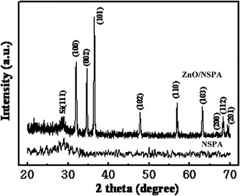
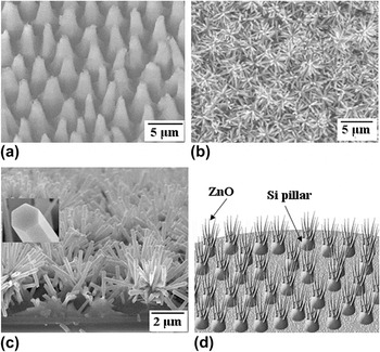
The XRD spectra for NSPA and ZnO/NSPA are depicted in Fig. 1. Here a broadened Si (111) diffraction peak was observed for NSPA, and a group of diffraction peaks corresponding to pure hexagonal phase ZnO (wurtzite-type; space group, P63mc) with calculated lattice parameters of a = 3.247 Ả and c = 5.201 Ả were observed for ZnO/NSPA. This directly proved the growth of crystalline ZnO onto NSPA, i.e., good quality ZnO NWs is achieved. Figure 2 (a) represents the typical surface morphology of NSPA obtained by FE-SEM, where a regular pillar array could be observed. After the growth of ZnO NWs, the Si pillars branched out and the tree-like nanostructures were formed. The top image of ZnO/NSPA given in Fig. 2(b) disclosed that numerous ZnO NWs with a high density over a large area and a diameter ∼200 nm could be seen, and the whole surface of NSPA was almost covered by ZnO NW bundles. The inset of Fig. 2(c) shows a high-magnification image of a ZnO NW, showing the hexagonally faceted morphology with a diameter of ∼195 nm. Judging from the magnified cross-sectional image of ZnO/NSPA (Fig. 2(c)), the length of ZnO NWs was estimated to be about 1.2–2.0 μm, and the NWs were grown densely and randomly at the top sites of the Si pillars, although sparsely distributed growth sites were also found on the lateral surfaces of the pillars and in the valleys between the pillars. This means that the growth of ZnO NWs on NSPA was a site-selective growth process, and it is natural to deduce that the microstructure and surface chemical properties of NSPA would play key roles in leading to the formation of the regularly patterned ZnO/NSPA. It should be noted from Fig. 2(c) that even after the ZnO growth, the pillar array of NSPA was still well-kept. On the basis of the above analysis, the structure of ZnO/NSPA could be illustrated by the diagrammatic sketch given in Fig. 2(d). Here, almost no ZnO NW bundles were observed beside the upside of each Si pillar, and ZnO/NSPA could be viewed as a complex and unique nanoheterostructure.
X-ray diffraction patterns of ZnO/nanoporous silicon pillar array (ZnO/NSPA) and NSPA.

Field emission scanning electron microscopic images of (a) NSPA, (b) ZnO/NSPA, (c) cross-sectional image of ZnO/NSPA, and (d) the schematic representation of ZnO/NSPA. The inset of (c) shows a high-magnification image of a ZnO NW. The images of (a) was taken with the sample being tilted at an angle of 40°.

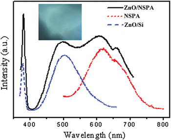
Figure 3 presented the PL spectra of ZnO/NSPA measured at room temperature, together with those of NSPA and ZnO/Si for comparison. Here ZnO/Si is obtained by the similar preparation method to ZnO/NSPA just by replacing NSPA with p-type single crystal silicon wafer, and the vertically well-aligned ZnO NWs could be observed on the substrate. All PL spectra were measured under a UV irradiation of 340 nm. The ZnO/NSPA nanoheterostructure exhibited a PL spectrum ranging from 350 to 750 nm, and four distinct PL bands, peaked at ∼381, ∼497, ∼611 and ∼658 nm, were observed. The appearance of the sharp narrow UV peak is an indication of the good quality of the ZnO NWs; i.e., a well-defined material with a bandgap of ZnO is achieved. It should be noted that the later three strong and broadened PL bands covered essentially the entire visible spectral region having the impact of white light. This indicates that ZnO/NSPA might be a potential light source for solid-state white light emission. In fact, the strong quasi-white light emission from this ZnO/NSPA system has been observed from the fluorescence microscopy image of a ZnO/NSPA layer excited by 325 nm laser radiation, as shown in the inset of Fig. 3, and it also provided another candidate path for future Si-based solid-state lighting devices or Si ultralarge-scale integrated circuits with optics to overcome the speed limitation of electrical interconnects and to add extra functionalities on Si chips. To realize the essential requirements for practical solid-state white light emitting devices, the origin of these emission bands must be first clarified.
The room temperature photoluminescence (PL) spectra obtained for the bare NSPA, ZnO nanowires grown on single crystal Si wafers, and ZnO nanowire bundles grown on NSPA, excited by 340 nm ultraviolet. The inset shows the bright fluorescence microscopy image of a ZnO/NSPA layer excited by 325 nm laser radiation.

As can be seen in Fig.3, the PL spectrum of ZnO/NSPA is different from both NSPA and ZnO/Si, which exhibited two red PL bands centered at ∼660 and ∼618 nm for NSPA, and one blue-green PL band and one UV PL band centered at ∼501 and ∼378 nm for ZnO/Si, respectively. Comparing the two red PL bands from both NSPA and ZnO/NSPA, it can be seen that the difference between the corresponding peak positions is very small, ∼7 and ∼2 nm, respectively. And calculating from their multi-peak Gauss fitting curves, the full width at half maximum (FWHM) of the corresponding peaks are almost the same, ∼93 and ∼61 nm, respectively. Therefore, it is reasonable to deduce the emitters contributing to the two red PL bands of ZnO/NSPA should be directly originated from the NSPA substrate beneath the upper ZnO NW layers, and most probably, they may have the same emission processes. As discussed in Ref.Reference Xu and Li12, the two red emission bands observed in the PL spectrum for NSPA could be well explained by the quantum confinement-luminescence center model, that is, the excitation processes for two red emission bands are identical, whereas the emission process mainly occurred through luminescence centers (LCs) located at the surface of Si nanocrystallites (nc-Si) or in the SiOx layer encapsulating nc-Si. The peak intensities of the two red PL bands from ZnO/NSPA were a little higher than those from NSPA, and this might be due to the generation of ∼381 nm UV emission from ZnO NWs, which will enhance the intensity of the excited UV.
Both the sharp UV emission band centered at ∼381 nm with FWHM ∼10 nm and the broadened blue-green emission band at ∼497 nm with FWHM ∼78 nm observed in the PL spectrum of ZnO/NSPA were most notably similar to that of ZnO/Si. Considering that single-crystal Si has one major disadvantage, an indirect bandgap that makes it a poor light emitter, indicated directly that whatever the detailed mechanism might be, the two observed PL emission bands must have originated from ZnO NWs. In fact, the origin of the narrow UV emission band peaked at ∼381 nm is attributed to the near-band-edge transition that is responsible for the recombination of free excitons through an exciton–exciton collision process in ZnO.Reference Ku, Huang, Cheng, Lin and Lee17–Reference Li, Fang, Su, Li, Wu and Zhao19 As for the broad blue-green PL band centered at ∼497 nm, it should be related to the deep-level defect in ZnOReference Chang, Jian, Lee, Lin and Juang11, Reference Kasai20–Reference Liu, Liu, Yang, Wang, Ma, Zhang, Lu, Shen and Fan22; because a similar broad PL band centered at ∼500 nm has been observed in various ZnO nanostructures synthesized under oxygen-deficient conditions, and the origin is ascribed to the radiative recombination of electrons with holes trapped in singly ionized oxygen vacancies in the bulk of ZnO NWs.Reference Kasai20–Reference Liu, Liu, Yang, Wang, Ma, Zhang, Lu, Shen and Fan22 Moreover, our XPS data of ZnO/NSPA (not shown here) has indicated that the atomic ratio between Zn and oxygen was about 1.00:0.92, which inferred that large quantities of oxygen vacancies (V o*) might have been formed on the surface of ZnO NWs. During the preparation process, the number of molten Zn atoms increase at higher temperature, combined with oxygen to form ZnO. Considering that there should be a balance between the melting rate of Zn and the growth rate of ZnO NWs, high temperature requires more oxygen for the growth of the ZnO NWs. But the constant flow rate of oxygen even at higher temperature leads to oxygen deficiency. In our experiment, because ZnO NWs are fabricated under the low-pressure system and at 575 °C, a quantity of V o* can also easily be produced. The surface-trapped hole can tunnel back into the nanocrystal, where it recombines with an electron in a V o*, resulting in the creation of a V o** centre, which is the recombination centre for the blue-green emission. Therefore, it is reasonable to attribute the blue-green PL band from ZnO/NSPA to the transition of the photoexcited electrons from the shallow level close to the conduction band edge of ZnO to a deeply trapped hole (a V o** centre).Reference Dijken, Meulenkamp, Vanmaekelbergh and Meijerink21, Reference Liu, Liu, Yang, Wang, Ma, Zhang, Lu, Shen and Fan22 Moreover, this peculiar morphology with small length scales and large surface-to-volume ratio for ZnO NWs may also be assigned to the strong blue-green emission observed. These observations indicate that both ZnO NWs and NSPA contribute to the luminescence, although it seems that at least the emission processes corresponding to the two red PL bands, the blue-green and UV emission bands, were accomplished by NSPA and ZnO NWs separately, and no quantum coupling between the two subnanosystems occurred. The PL spectrum is almost the same even after a year, which reveals the stability of the ZnO/NSPA nanoheterostructure. The clarification on the PL origins of ZnO/NSPA might have provided a base for realizing PL adjustability.
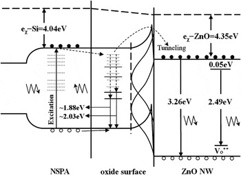
For a better understanding of the carrier dynamics associated with the light emission of ZnO/NSPA, we propose a model to explain the PL spectra with the band energy diagram as shown in Fig. 4. Here, χ Si = 4.01 eV and χ ZnO = 4.35 eV denote the electron affinity of silicon and ZnO, respectively. As discussed in Ref.Reference Xu and Li12, the surface of NSPA has been oxidized and the formed oxide is in the states of silicon monoxide and silicon dioxide, which would lead to the formation of two kinds of LCs. Therefore, in this model, we have shown the formation of the SiOx (x ≤ 2) structure at the interface of ZnO and NSPA. It is known that the bandgap energies of Si, NSPA (considered as a material consisting of nc-Si encapsulated by the SiOx shells), and ZnO are ∼1.12 eV, ∼3.15 eV, and ∼3.35 eV, respectively.Reference Willander, Nur, Bano and Sultana10, Reference Xu and Li12 Therefore, it is clear that the band gap energy of NSPA is adjusted in between the band gaps of Si and ZnO, and the active NSPA layer would play a key role in the optical properties due to the high interface state density. The SiOx layer works as a wavelength converter at a higher wavelength. The emission peaks at ∼611 nm (2.03 eV) and ∼658 nm (1.88 eV) could be explained by supposing that the emission process mainly occurred through two kinds of LCs located at the surface of nc-Si or in the SiOx layer encapsulating nc-Si.Reference Xu and Li12 Simultaneously, because of the larger surface-to-volume ratio of the NSPA layer, a band bend is formed at the ZnO/NSPA interface, and the direct tunnel transfer of photo-excited carriers across the energy barrier from NSPA to the conduction of ZnO could be due to the narrowing of the barrier. The carriers tunneling to the ZnO conduction will recombine with deep level V o** in the band gap,Reference Dijken, Meulenkamp, Vanmaekelbergh and Meijerink21–Reference Singh, Singh, Kanjilal, Agarwal and Mehra23 causing emission of a blue-green light band at ∼497 nm (2.49 eV). The tunneling of the conduction band electrons at the surface decreases because it takes place between localized states, whereas the surface trapping of the conduction band electrons involves a delocalized state. Therefore, the emission around ∼381 nm (3.26 eV) is attributed to the annihilation of bound free excitons, i.e., electron–hole pairs from the excited state to the initial state.Reference Dijken, Meulenkamp, Vanmaekelbergh and Meijerink21, Reference Liu, Liu, Yang, Wang, Ma, Zhang, Lu, Shen and Fan22
The schematic plan to illustrate the PL mechanism of ZnO/NSPA.

IV. CONCLUSIONS
In summary, a novel ZnO/Si nanoheterostructure was prepared by growing ZnO NWs onto NSPA through a self-catalytic thermal evaporation and vapor-phase transport method; here, numerous ZnO NW bundles were grown at the top sites of each Si pillar. Quasi-white light photoluminescence on ZnO/NSPA were realized by combining the UV band-edge transition and blue-green Vo-related surface state emission from ZnO and two red PL bands from the NSPA substrate. A model-based band diagram is proposed to illustrate the combined emission. The realization of quasi-white light PL in ZnO/NSPA might have provided another candidate path for future lighting devices, such as all solid and wide wavelength white light-emitting diode or Si ultralarge-scale integrated circuits with optics to overcome the speed limitation of electrical interconnects and to add extra functionalities on Si chips.
ACKNOWLEDGMENT
This work was supported by the Doctoral Fund of Ministry of Education of China (Grant No. 20090010120014), the Beijing Natural Science Foundation (Grant No. 1103033), and the Fundamental Research Funds for the Central Universities.