I. INTRODUCTION
Aluminum-doped zinc oxide (ZnO:Al or AZO) is the leading candidate for the replacement of indium tin oxide (ITO) for applications requiring low cost transparent conductors. It is known that the electrical and optical properties of transparent conducting oxide (TCO) thin films, including ITO,Reference Liu, Avrutin, Izyumskaya, Özgür and Morkoç1–Reference Kumar, Raju and Subrahmanyam3 fluorine-doped tin oxide,Reference Amanullah, Pratap and Babu4–Reference Rakhshani, Makdisi and Ramazaniyan6 gallium-doped zinc oxide,Reference Fortunato, Gonçalves, Assunção, Marques, Águas, Pereira, Ferreira and Martins7, Reference Minami8 and AZO,Reference Dong, Fang, Wang, Guan and Zhao9–Reference Liang, Fan, Cai, Zhang and Zheng11 are strongly dependent on film thickness. ITO is often preferred for its excellent properties, but its cost is high due to increasing demand for displays, solar cells, and smart windows. AZO, in contrast, is produced from abundant, low-cost, and nontoxic materials. One approach to lower cost is reducing film thickness, and indeed ITO films exhibit relatively low resistivity even for film thickness less than 100 nm.Reference Lee and Ok Park12 Further savings could be realized if high quality AZO was available. However, the electrical properties of sputter-deposited AZO thin films deteriorate quite dramatically when film thickness is less than 150 nm. Though much effort has been made to obtain high quality AZO films, achieving low resistivity and high mobility AZO films thinner than 100 nm is still a tough challenge.
Various methods have been used to prepare AZO thin films, among which magnetron sputtering (MS)Reference Agashe, Kluth, Hupkes, Zastrow, Rech and Wuttig13–Reference Tominaga, Umezu, Mori, Ushiro, Moriga and Nakabayashi22 and pulsed laser deposition (PLD)Reference Di Trolio, Bauer, Scavia and Veroli23–Reference Tanaka, Ihara, Miyata, Sato and Minami28 are common. Less common is filtered cathodic arc deposition (FCAD), but it has been widely used to fabricate high quality metal oxide thin films due to the high ion energy and high ionization rate of the condensing plasma.Reference Tay, Zhao and Chua29 This makes it a promising technique for growing high quality thin films with small thicknesses. Compared with PLD, which also produces a highly ionized flux of material, FCAD is easier to scale up and more cost effective, which is critical for large-area applications. AZO thin films have been prepared by FCAD by several groups in the pastReference Anders, Lim, Yu, Andersson, Rosén, McFarland and Brown10, Reference Goldsmith30–Reference Zhitomirsky, Çetinörgü, Adler, Rosenberg, Boxman and Goldsmith33; however, there is still lack of a systematic study on the effect of film thickness for AZO, especially for film thickness less than 100 nm. In this study of thin AZO film deposition, we utilize the kinetic and potential energy of the arriving atoms and/or ionsReference Anders34, Reference Anders35 to produce material with high carrier mobility. We will show that arc-deposited thin AZO films have properties comparable to the more expensive ITO films.
II. EXPERIMENT
AZO thin films were deposited on glass substrates by direct current (dc) FCAD. The cathode material was zinc doped with aluminum (4 at.% Al, as specified by the manufacturer), which gave Al concentrations in the films of 1.0 ± 0.3 at.% as measured by Rutherford backscattering spectroscopy. At this time it is still unclear why the aluminum concentration in the films is surprisingly low. The cathode–substrate distance was fixed at about 300 mm, and the arc current was set to 70 A. The zinc–aluminum plasma passed through a 90°-bent open coil electromagnetic filter to remove most of the macroparticles.Reference Anders36 Films made by filtered cathodic arc are free of haze to the eye; however, we identified about 50–100 macroparticles per square millimeter under a 500× optical microscope. Macroparticles are known to exhibit a fractal size distribution, with the largest particles 1–10 μm in diameter.Reference Anders37
Borosilicate microscope glass slides were used as substrates. Before mounting them on the substrate holder, the substrates were gently cleaned using commercial glass detergent (Liqui-Nox) and thoroughly rinsed with water. Remaining water droplets were blown off by dry nitrogen; no visible residues could be seen on the glass. The substrates were heated up to 425 °C using a 4-lamp radiative heater once the chamber was cryogenically pumped to a base pressure about 5 × 10⁻⁶ Torr. Prior to deposition, the substrates were exposed to a 75 W oxygen plasma from a constricted plasma sourceReference Anders and Kühn38 for 2 minutes to burn off any hydrocarbons, if present on the glass surface. Then the partial pressure of oxygen was set to 5 mTorr before growth using a mass flow controller. Once ignited, the metal arc plasma consumed enough oxygen to drop the pressure in the chamber to 2.5–3.5 mTorr. This is a well-known gas pumping effect by compound films deposition. The fluctuations in the partial pressure are due to the typical fluctuations of the arc process itself. The deposition rate was in the range 4.1±0.4 nm/s.
Film thickness was measured using step profilometry, and surface morphology was studied with a Veeco MultiMode AFM (Veeco, Plainview, NY) in tapping mode. Film structure was investigated by a Bruker x-ray diffractometer (Bruker AXS Inc., Madison, WI) equipped with an area detector. A LaB6 powder diffraction standard was used to ensure calibration of the 2θ angle and to measure the instrumental broadening. It was found that the uncertainty in the 2θ position was ±0.025° after calibration by sprinkling the LaB6 directly on top of several samples and comparing repeated measurements. A Perkin Elmer Lambda 950 dual beam photospectrometer (PerkinElmer, Waltham, MA) was used for transmittance measurements in the wavelength range 200–2500 nm. The electrical properties of the films were characterized by Hall measurements in the Van der Pauw geometry using an Ecopia HMS-3000 system. (Bridge Technology, Chandler Heights, AZ)
III. RESULTS
A. Film structure
X-ray diffraction (XRD) patterns of AZO films as a function of thickness: the XRD intensity from the (002) peak increases with increasing thickness as more AZO is available to diffract the incoming beam. The films are all of hexagonal wurtzite crystal structure with the c-axis perpendicular to the substrate. Only the (002) diffraction peak of ZnO appears and no metallic Zn or Al characteristic peaks are observed in the XRD analysis. Also, no signs of any Al2O3 or spinel phases (ZnAl2O4) can be seen.
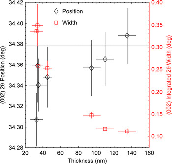
Figure 1 shows the position of the (002) peak and its integrated width as a function of film thickness. The (002) peak position shifts to higher diffraction angle as the films get thicker and tends toward the bulk ZnO value of 34.378°. The c-lattice parameter calculated from the (002) peak position using the Bragg equation is larger than that of the bulk ZnO for films less than 110-nm thick. Using the biaxial strain model,Reference Maniv, Westwood and Colombini20 a compressive in-plane stress of 1.3 ± 0.5 GPa was calculated to be present in the 33-nm film.
ZnO (002) x-ray diffraction peak position (black diamonds) and its integrated width (red squares) with error bars in both directions for all the aluminum-doped zinc oxide (AZO) samples.

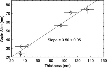
Grain size in the (002) direction calculated from the Scherrer equation using the integrated width (corrected for the machine broadening) of the (002) peak is shown in Fig. 2. The width was extracted by fitting the peak with a Voigt line shape. It is observed that the grain size increases almost linearly with increasing film thickness and an average grain size of 30 nm was observed in the 33-nm film.
Grain size in the (002) direction for AZO thin films grown at 425 °C and 2.5–3.5 mTorr with arc current at 70 A as a function of film thickness.

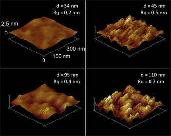
Atomic force micrographs of the surface morphology of AZO films with different thicknesses are shown in Fig. 3. Continuously packed and uniform features are observed in all the AZO films. Even for the 34-nm film, no vacancy or island structures are observed. The root mean square (RMS) roughness (R q) is less than 1 nm for films thinner than 100 nm, which is close to the R q of the glass substrate.
Atomic force microscope images of AZO films of different thicknesses. Thickness (d) and RMS roughness (R q) are shown above each image.

B. Electrical properties
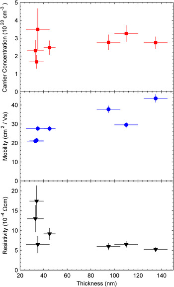
Figure 4 shows the electron concentration (n), resis-tivity (ρ), and mobility (μ) of AZO thin films as a function of film thickness. The electrical properties of AZO thin films show trends that are related to the structural properties: the resistivity quickly decreases and the mobility quickly increases with increasing thickness. For films less than 45-nm thick, the mobility was 20–30 cm2/Vs, which is comparable to mobilities of much thicker sputter-deposited films. In particular, the 35-nm-thick films exhibited a mobility of 28 cm2/Vs and a low resistivity of 6.5 × 10⁻⁴ Ωcm. Resistivity as low as 5 × 10⁻⁴ Ωcm and a carrier mobility as high as 44 cm2/Vs were obtained in the 135-nm film.
Electrical properties of AZO films grown at 425 °C and 2.5–3.5 mTorr with arc current at 70 A as a function of film thickness.

C. Optical transmittance
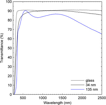
The optical transmittance of the two AZO thin films with thicknesses of 34 and 135 nm is shown in Fig. 5. The mean visible (400–750 nm) transmittance of AZO/glass stacks was over 85%, and the maximum transmittance was greater than 90%. The decrease of transmittance in the near infrared region results from the increase of reflectance and absorption which is attributed to the plasma resonance of the electron gas in the conduction band.Reference Jin, Hamberg and Granqvist39
Optical transmittance of AZO/glass stacks. The glass is 1-mm thick and film thickness is shown in the legend.

IV. DISCUSSION
As it is well known, and often demonstrated, that film quality improves with increasing thickness, and our study is not an exception. The study quantifies what can be achieved using the kinetic and potential energy of the cathodic arc process when trying to optimize thin (100 nm or less) films—because those films are of great interest to many applications.
From Fig. 1, we can see how fast the integrated width of the (002) peak decreases, indicative for the improvement of the crystalline quality of AZO thin films. The compressive stress is rapidly released with increasing film thickness and the films are nearly stress-free when thicker than about 150 nm. This may be attributed to the accumulation of heat right at the surface where film growth occurs. In contrast to deposition by MS and other PVD techniques, filtered cathodic arc delivers fully ionized plasma to the substrate surface. Each of the condensing ions brings substantial energy to the growth process. Most notably, the average kinetic energy of zinc ions is about 36 eV and its potential (ionization energy) is 9.39 eV plus the cohesive energy of 1.35 eV.Reference Anders34 That is, each arriving ion brings roughly 47 eV to the surface, most of which ends up in heat. This enhances the surface atom mobility and provides an annealing effect without having to excessively heat the entire glass substrate.
Figure 2 indicates that the average vertical, c-axis grain size is half the film thickness for such films. The relatively larger grain size for thin films obtained by filtered arc deposition compared to that of other techniques is beneficial for the Hall mobility of conduction electrons—a key property for the performance of TCOs.Reference Dong, Fang, Wang, Guan and Zhao9, Reference Suzuki, Nakamura, Michihata, Aoki, Matsushita and Okuda27 The relatively large, c-axis aligned grains are a consequence of competitive growth with surface-enhanced temperature and self-ion assistance.Reference Petrov, Barna, Hultman and Greene40 The low roughness (R q values) of the arc-deposited thin films is well suited for applications in which the work function is critical as it is extremely sensitive to the state of the surface.Reference Betz, Olsson, Marthy and Escolá41, Reference Klöppel, Kriegseis, Meyer, Scharmann, Daube, Stollenwerk and Trube42
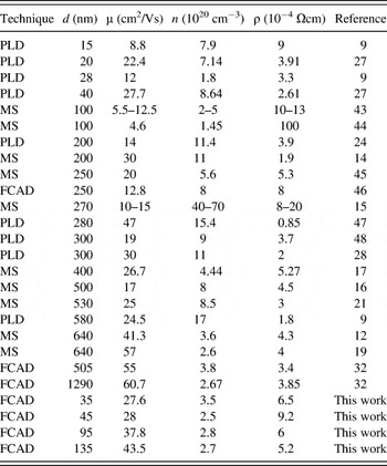
Table I shows the electrical properties of the arc-grown AZO films compared to values reported for several growth techniques and film thicknesses. For AZO films with a thickness less than 45 nm, the electrical properties of films prepared by FCAD in this study are comparable to that of optimized AZO films grown by PLD, although PLD resulted in greater surface roughness.Reference Suzuki, Nakamura, Michihata, Aoki, Matsushita and Okuda27 Arc-deposited films less than 150-nm thick compare very well to much thicker AZO films prepared by MS at low growth rates.Reference Agashe, Kluth, Hupkes, Zastrow, Rech and Wuttig13, Reference Fang, Li and Yao17, Reference Jäger, Szyszka, Szczyrbowski and Bräuer19, Reference Szyszka21, Reference Tominaga, Umezu, Mori, Ushiro, Moriga and Nakabayashi22, Reference Konishi, Noda, Harada and Sasakura45 For comparison, much thicker films deposited by the filtered arc technique are also included in Table I. The lowest resistivity of 3.4 × 10⁻⁴ Ωcm and highest mobility of 60 cm2/Vs were reported in our previous study.Reference Mendelsberg, Lim, Zhu, Wallig, Milliron and Anders32
Comparison of electrical properties of aluminum-doped zinc oxide thin films of various thicknesses prepared by pulsed laser deposition (PLD), magnetron sputtering (MS), and filtered cathodic arc deposition (FCAD).

Cathodic arcs have a small burning voltage of roughly 20 V and therefore cannot produce the high energy negative oxygen ions that are commonly produced in reactive magnetron sputter deposition of AZO. Although the moderate energy of arc ions (up to 40 eV) are beneficial in terms of film quality,Reference Mendelsberg, Lim, Zhu, Wallig, Milliron and Anders32, Reference Ghafoor, Eriksson, Persson, Hultman and Birch49, Reference Tungasmita, Persson, Hultman and Birch50 the high energy ions of sputter system of typically several 100 eV (up to the magnetron voltage of ∼500 V) are detrimental because they generate numerous defects. For arc-grown AZO films, even very thin layers are subjected to significant low-energy ion bombardment during growth, which we have shown improves their structural and electronic properties compared to very thin sputter-deposited films.
The AZO films prepared by dc FCAD are highly transparent as was shown in Fig. 5. The high electron mobility ensures that high-conductivity material is obtained even as the concentration of donors is only to 1 at.%. This low concentration, in turn, shifts the plasma edge (reduces the plasma frequency) such that nearly the entire solar spectrum can be transmitted, and not only the visible part of the spectrum. Therefore, arc-grown AZO is potentially suitable for high efficiency, multijunction solar cells that also harvest the solar infrared.
V. SUMMARY AND CONCLUSIONS
The favorable energetics of the filtered cathodic arc technique leads to thin AZO films that are superior to sputter-deposited films, which makes them an interesting alternative to the more expensive thin ITO films. For AZO films less than 45-nm thick, a relatively high mobility of 20–30 cm2/Vs and a relatively low resistivity of 6–20 × 10−4 Ωcm have been demonstrated. Such values are comparable to much thicker films fabricated by MS. Even thinner films, about 35-nm thick, exhibited a Hall mobility of 28 cm2/Vs and a low resistivity of 6.5 × 10⁻⁴ Ωcm. As the film thickness is increased, larger, c-axis-aligned grains are observed leading to resistivity as low as 5.2 × 10⁻⁴ Ωcm and mobility as high as 44 cm2/Vs for a 135-nm film. Such arc-deposited AZO films have a relatively low carrier concentration, thus the plasma edge is shifted to longer wavelengths and nearly the entire solar spectrum is transmitted. This makes this material of interest to high efficiency solar cells. Films thinner than 100 nm have very low RMS roughness of order 1 nm, which can be important to some electronic applications.
ACKNOWLEDGMENTS
The authors thank J. Wallig, K.M. Yu, and D.J. Milliron for their contributions to this work. Research was supported by the LDRD (Laboratory-Directed Research and Development) Program of Lawrence Berkeley National Laboratory, by the Assistant Secretary for Energy Efficiency and Renewable Energy, Office of Building Technologies under U.S. Department of Energy Contract No. DE-AC02-05CH11231. Portions of this work were performed as a User Project at the LBNL Molecular Foundry, which is supported by the Office of Science, Office of Basic Energy Sciences, under the same contract.