I. INTRODUCTION
Along with the development of wireless communication system, microstrip antenna technology is also developing day by day. In recent years, microstrip patch antennas are widely used in many practical applications such as radar technology, satellite communication, mine detection, and high-speed wireless local area network (LAN), due to their inherent advantages of low-profile, light weight, low-cost, and ease of integration [1].
When polarization matching is not necessarily assured for a given orientation of linearly polarized transmitter and receiver antennas, use of the circular polarization (CP) system is more preferable than linear polarization. This is the case, for example, with low-Earth orbit or unstabilized satellites, where the antennas are randomly oriented [Reference Davies and Smith2]. Similarly, radio-frequency identification (RFID) reader systems usually use CP in order to enable communication with RFID tags, whatever their orientation is [Reference Garcia, Arriola, Casado, Chen, Sancho and Valderas3]. In radar technology, CP is used to minimize interference from rain.
Among different methods to generate CP, the use of linear polarization patch elements in array configuration can be a good technique to excite circularly polarized signals. Such type of technique is used in [Reference Huang4, Reference Iwasaki, Nakajima and Suzuki5] for CP. In [Reference Huang4], to generate CP, linearly polarized array elements are arranged in a 2 × 2 square or grid configuration with element angular orientation, and feed phase arranged in either a 0°, 90°, 0°, 90°, or a 0°, 90°, 180°, 270° fashion. In this case, four array elements are required for CP. Moreover, only microstrip lines are used to design feed circuit. Dual orthogonal feed CP array antenna structure with microstrip–slot feed network is reported in [Reference Rahman, Hossain, Hossain and Chowdhury6]. In [Reference Shahabadi, Busuioc, Borji and Safavi-Naeini7], a Ku-band CP array antenna benefiting from low-loss waveguide feed network is demonstrated. Although it provides high efficiency, the structure of the antenna is complex. In recent years, several CP array antennas using sequential rotation technique have been presented with improved axial ratio bandwidth [Reference Jazi and Azarmanesh8–Reference Evans and Sambell11].
Several designs using single-patch element have been proposed for CP. In these designs, the perturbation technique is applied to excite CP, including a square microstrip antenna with four slits in diagonal directions with a pair of truncated corner [Reference Gautam, Benjwal and Kanaujia12] or a hexagonal microstrip antenna by inserting slits at the boundary with truncated corners [Reference Qian and Tang13], inserting cross-slot of unequal arm lengths [Reference Iwasaki14, Reference Lu, Tang and Wong15], by embedding symmetric cross-shaped slot along one of the diagonal axis [Reference Chen and Qing16] or by introducing asymmetric-circular-shaped slots along the diagonal directions with four symmetric slits in orthogonal directions [Reference Chen and Qing17], by inserting asymmetric slits in diagonal directions onto the microstrip patch [Reference Qing and Chen18]. E-shaped CP patch antenna with two RF PIN diodes added in the slots region is presented in [Reference Khidre, Lee, Yang and Elsherbeni19]. In [Reference Lin, Zhang, Jiao, Zhang and Xue20], a CP microstrip antenna that is excited by three central symmetrical feeds with equal amplitudes and relative 120° phase shifts is proposed.
Tuning stub or a bent tuning stub can be an effective way to excite CP due to the frequency-tuning capability of the tuning stub. This design concept has been successfully applied to a circular patch [Reference Wong and Lin21, Reference Wong and Chen22], a square-ring patch [Reference Chen, Wu and Wong23], and a triangular patch [Reference Lu and Wong24]. To increase gain, circularly polarized patch elements can be arranged in array and this type of structure is presented in [Reference Huang25].
In this paper, a circularly polarized array antenna is proposed using both-sided MIC technology where CP is achieved having a 2 × 2 array composed of single feed linearly polarized patches. The patches are arranged in such a way that the resultant array radiation is circularly polarized. The feed network is designed using both microstrip lines and slot line instead of using only microstrip lines. In the proposed structure, the antenna parameters are optimized to achieve excellent performance. Effect of changing each antenna parameter is investigated that helps to understand the characteristics of the array antenna.
II. BOTH-SIDED MIC TECHNOLOGY FOR ANTENNA DESIGN
The conventional microstrip array antenna is shown in Fig. 1. Feed circuits for the conventional microstrip array antenna are usually composed of the microstrip line. Since all the feeding circuit is connected in parallel, many matching circuits are required. As a result, the feeding circuit layout for array antenna becomes complicated and the line length becomes much longer. These cause the array antenna to increase the feeding loss as well as the undesired radiation, such as the cross-polarized radiation [Reference Kodama, Nishiyama and Aikawa26].
Conventional microstrip array antenna (a) top view, (b) cross-sectional view (AA').

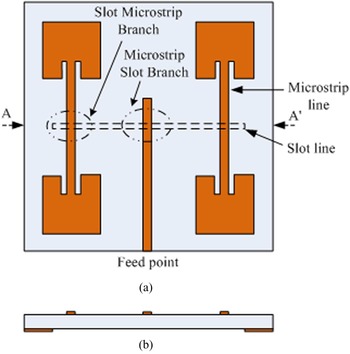
Such type of problems due to microstrip feed circuit can be overcome using both-sided MIC technology [Reference Aikawa and Ogawa27]. A microstrip array antenna using both-sided MIC technology is shown in Fig. 2. Using the both-sided MIC technology for the feeding circuits, the array antenna needs no impedance matching circuits and has very simple circuit configuration, which are mainly due to the excellent performances of both the microstrip–slot parallel branch circuit and the slot–microstrip series branch circuit. The feeding loss and the radiation loss can be expected to be small, as these branch circuits make the feeding circuit length small by eliminating the impedance matching circuit. Besides, this technology gives a chance to place several transmission lines such as microstrip lines, slot lines, coplanar waveguides on both the sides of the substrate.
Microstrip array antenna using both-sided MIC Technology: (a) top view, (b) cross-sectional view (AA').

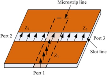
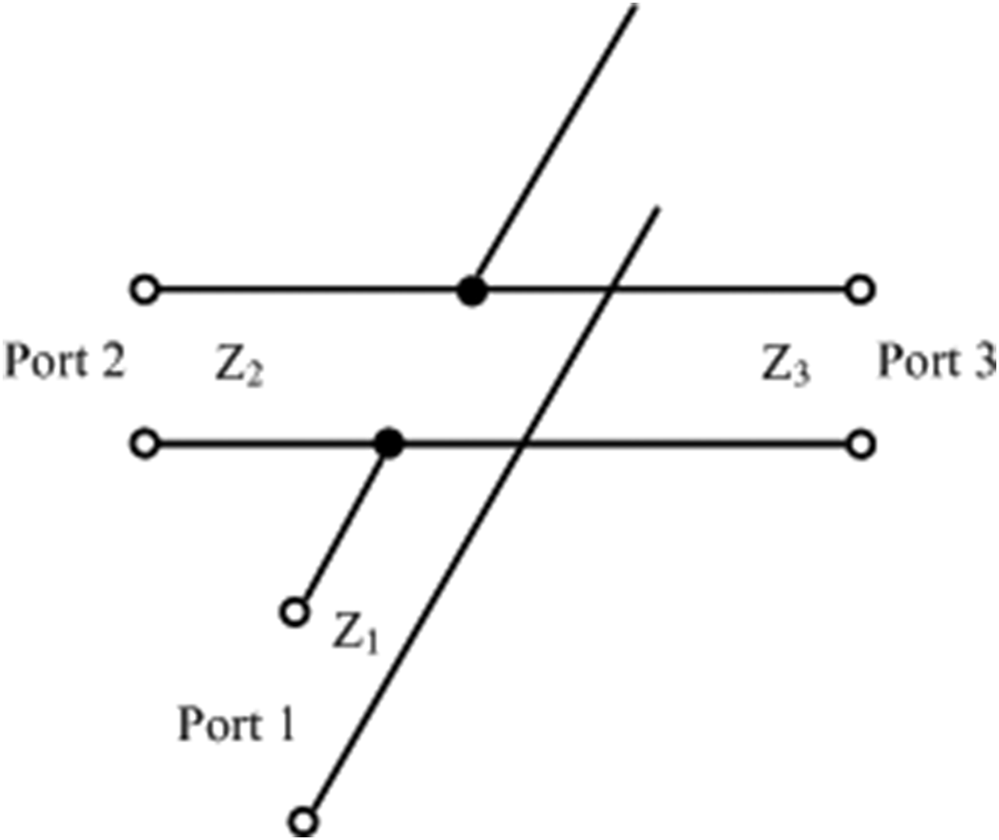
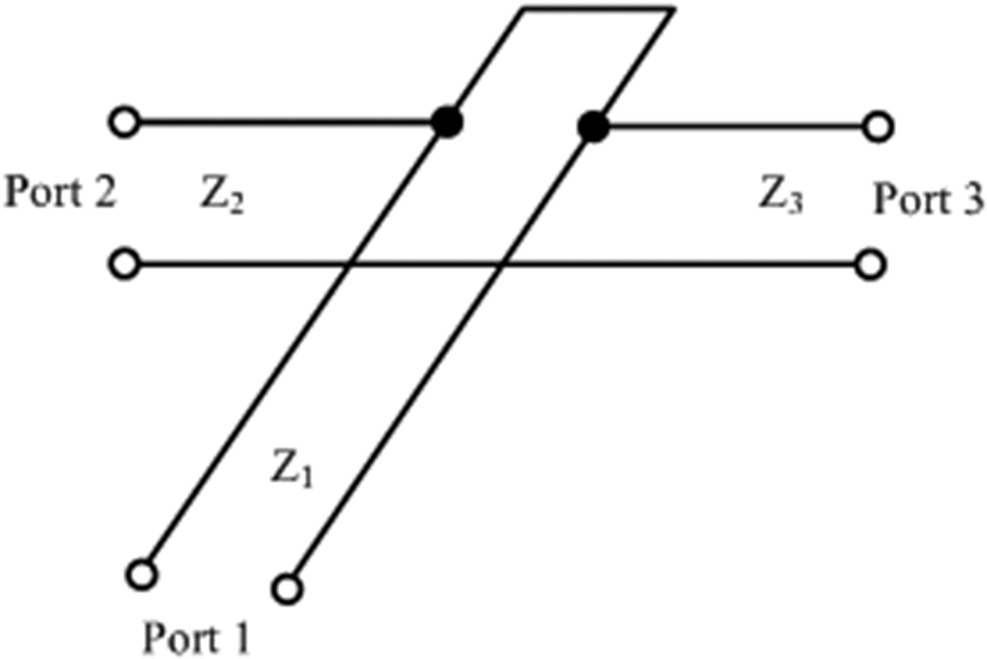
The microstrip–slot branch circuits are composed of microstrip line on the upper surface of a substrate and a slot line on the reverse side. The configuration and the equivalent circuit are shown in Figs 3 and 4, respectively.
Microstrip–slot branch circuit.

Equivalent circuit of microstrip–slot branch circuit.

The microstrip–slot branch circuit is a parallel power divider. The condition for impedance matching is, slot line impedance has to be double than microstrip line impedance (Z 2 = Z 3 = 2Z 1). Owing to the parallel coupling, two divided signals at the equal distance points from the branch point on the slot line have the same amplitude and are in phase in a very wide band [Reference Egashira, Nishiyama and Aikawa28].
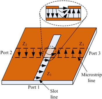
Figures 5 and 6 show the configuration and equivalent circuit for a slot–microstrip branch circuit, respectively. The condition for the impedance matching is, impedance of microstrip line has to be half than that of slot line (Z 2 = Z 3 = Z 1/2). Two output signals on the microstrip line at the equal distance points from the branch point have the same amplitude and are out of phase in a very wide band [Reference Egashira, Nishiyama and Aikawa28].
Slot–microstrip branch circuit.

Equivalent circuit of slot–microstrip branch circuit.

III. ARRAY ANTENNA GEOMETRY AND OPTIMIZATION
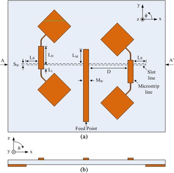
Figure 7 shows the complete geometry of the proposed array antenna. Its configuration consists of radiating square patches with a feed network designed using both-sided MIC technology. The design frequency of the four element array antenna is 10 GHz. The antenna is designed using Teflon glass fiber substrate with a thickness of 0.8 mm and dielectric constant of 2.15. The dielectric loss tangent of the substrate is 0.000194. Copper with a thickness of 0.018 mm is used as radiating plane and ground plane conductor. The obverse side of the substrate accommodates the radiating elements and the microstrip line of the feed network and the reverse side contains slot line of the feed network.
Layout of the proposed array antenna: (a) top view, (b) cross-sectional view AA'.

The dimension of each square patch is 9.46 × 9.46 mm2. Each patch element is linearly polarized. Distance among patches horizontally and vertically is kept same. Each patch element is placed at 45° angle with respect to the horizontal plane. The positional distance of one patch element on each side from the slot line (L H ) is determined in such a way that the feed line length is quarter wave length (λ\4) greater than that of the other patch element (L L ). This strategy ensures that the proposed array antenna is excited for circular polarized waves. In feed network, there are two types of branch circuits. One is the microstrip–slot branch circuit and another is the slot–microstrip branch circuit. The microstrip line of the microstrip–slot parallel branch circuit is fed by a microwave source through a 50 Ω co-axial cable probe. A quarter wave impedance transformer of 136 Ω (width = 0.3 mm) is used to match the each patch with the microstrip line of the slot–microstrip branch circuit.
A parametric analysis is performed to optimize the antenna parameters. It helps to investigate the effects of the different parameters on the impedance bandwidth and the axial ratio bandwidth. Moreover, this analysis provides some understanding of antenna characteristics that helps to tune the antenna for the best performance. The effects of varying the microstrip line width (M W ), slot line width (S W ) are studied. The impacts of changing the length of microstrip line extension over slot line in microstrip–slot branch (L M ), length of slot line extension from microstrip line in slot–microstrip branch (L S ), distance between microstrip–slot branch point and slot-microstrip branch point (D) are also investigated to understand the antenna characteristics. The study of the ratio between L H and L L between the two same side patches is also important to create 90° phase difference that helps to get optimized axial ratio performance from the proposed antenna. During the parametric analysis, except for the parameter of interest, the other parameters are kept constant.
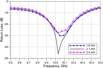
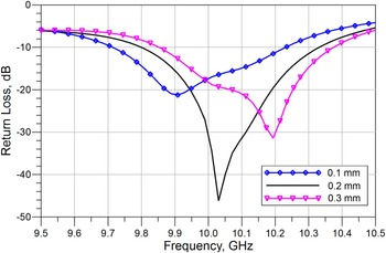
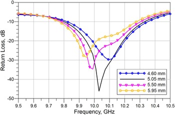
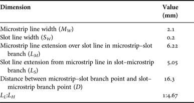
Figure 8 shows the variation of return loss for different values of microstrip line width (M W ). It is observed that the impedance bandwidth is less affected by it but it has great impact on impedance matching. Change of return loss for different slot line width (S W ) values is shown in Fig. 9. It is seen that with the increase of S W , the center frequency is shifted from lower frequency to higher frequency, although the impedance bandwidth is almost same for all values. By taking M W = 2.1 mm (54 Ω) and S W = 0.2 mm (107 Ω), the highest return loss is obtained. These optimized values also prove that the microstrip line impedance of the branch circuits should be half than that of slot line for the best performance. Hence, no matching circuit is required in the feed network like conventional microstrip feed network. For different values of L M and L S , the variations of return losses are plotted in Figs 10 and 11, respectively. Figures 10 and 11 demonstrate that the center frequency decreases with increasing values. The optimized values for the highest return loss are L M = 6.22 and L S = 5.05 mm. Figure 12 illustrates the return loss for different values of D. It is observed that with the increment of D value, the impedance bandwidth of the antenna starts to decrease. Although D = 15.3 mm gives a better operating bandwidth, D = 16.3 mm is chosen as an optimized value where return loss is at its best.
Return loss for different values of M W .

Return loss for different values of S W .

Return loss for different values of L M .

Return loss for different values of L S .

Return loss for different values of D.

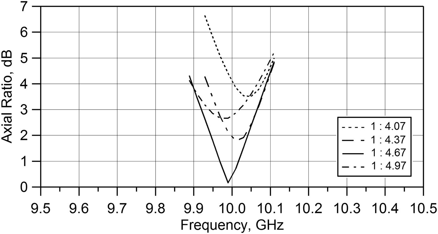
Variation of axial ratio for changing the ratio between L L and L M is shown in Fig. 13, while other parameters are fixed. From Fig. 13, it is found that the axial ratio is near to zero at L L : L M = 1:4.67 that means one of the patch is quarter wavelength ahead than other one of the same side and as a result the antenna is almost perfectly circularly polarized.
Variation of axial ratio for L L :L H .

IV. BASIC BEHAVIOR OF THE ARRAY
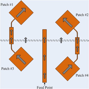
To generate circularly polarized waves, two orthogonal signals with 90° phase shift between them are needed. The basic behavior of the proposed circularly polarized array antenna can be explained using Fig. 14. When the patch #1 and the patch #4 are +45° linearly polarized, the patch#2 and the patch#3 are −45° linearly polarized. Combining the signals of patch#1, #4 and patch#2, #3, the modes are orthogonal.
Basic behavior of the array antenna.

Moreover, the length of feed lines is attuned according to Fig. 13 that there is a 90° phase shift between patch #1 and #4, and patch #2 and #3. Therefore, in the proposed array structure, two orthogonal signals are formed with 90° phase shift and as a result circular polarized signal is excited.
V. RESULTS AND DISCUSSIONS
The Method of Moments based advanced design system (ADS) of Agilent has been used to validate and evaluate the dimensions of the proposed circularly polarized array antenna. The results are also verified using another electromagnetic (EM) simulator, EMPro based on the FEM method. The various optimized parameter values of the antenna are listed in Table 1.
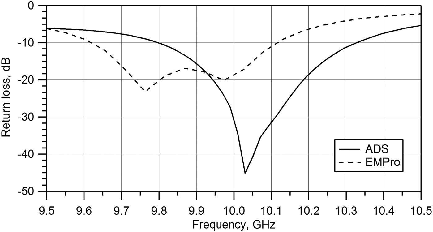
The return loss of the array antenna is shown in Fig. 15. The result using ADS indicates that the return loss is <− 10 dB from 9.8 to 10.34 GHz and it is the lowest close to the design frequency of 10 GHz. So the impedance bandwidth of the array is 5.36% with respect to the center frequency of 10.07 GHz. The impedance bandwidth (<− 10 dB) according to EMPro simulation result is 5.06%, from 9.63 to 10.13 GHz.
Input return loss of the array.

The Input impedance for the array (simulated by ADS) is illustrated in Fig. 16. A dip in the impedance locus is shown near at 10 GHz, which indicates that two resonant modes are excited at very close frequencies. This suggests that the fundamental mode in the present design is split into two near-degenerate resonant modes [Reference Wong29].
Input impedance of the array antenna.

It can be found that, when one of the patch elements is ahead by quarter wave length from the other patch of the same side, these two resonant modes can be excited with equal amplitudes and a 90° phase difference, resulting in circularly polarized radiation.
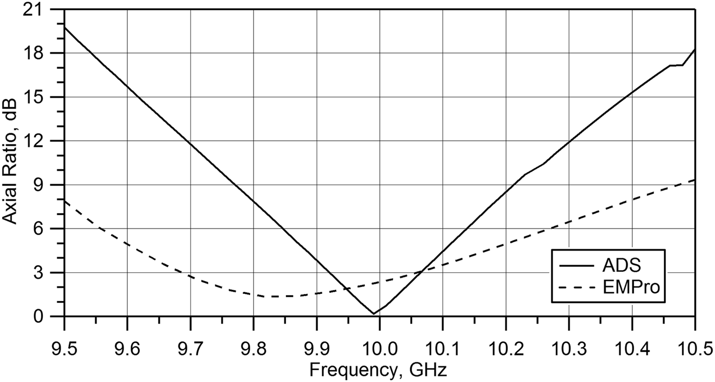
Figure 17 shows the axial ratio of the array. Axial ratio (using ADS) is <3 dB from 9.92 to 10.06 GHz and the minimum value is 0.164 at 9.99 GHz. So the 3 dB axial ratio bandwidth is about 1.4% with respect to the center frequency of 9.99 GHz, whereas the 3 dB axial ratio bandwidth from EMPro simulation result is 3.75% (from 9.68 to 10.05 GHz), which indicates that the proposed antenna can produce very good CP at design frequency.
Axial ratio of the array antenna.

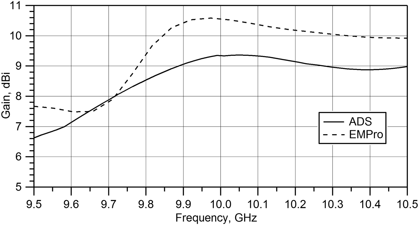
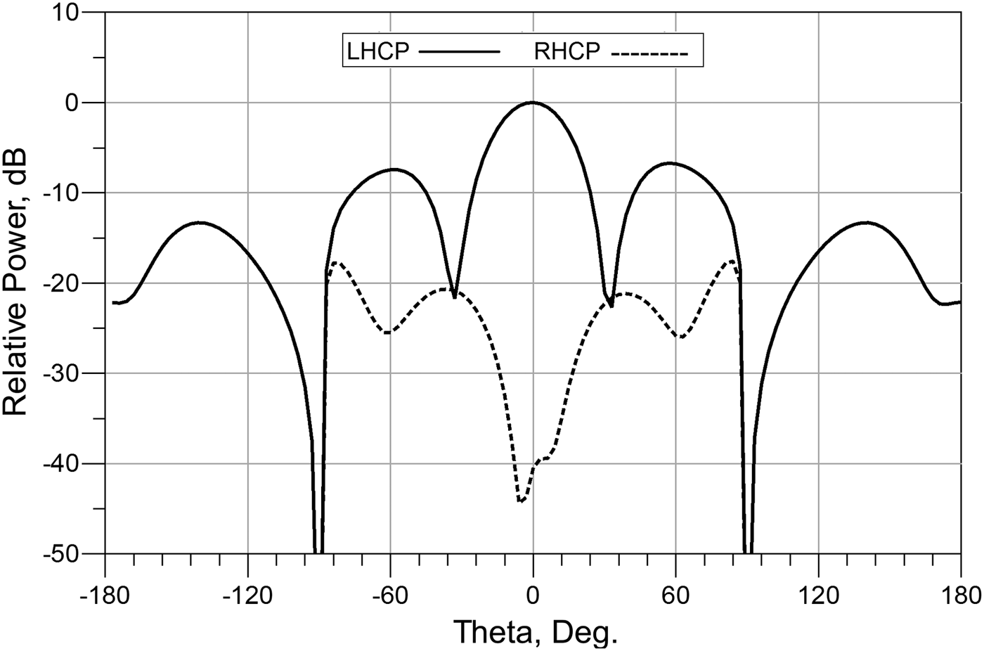
The gain of the array antenna is shown in Fig. 18. The peak gain simulated by ADS is 9.36 dBi at design frequency but using EMPro simulator, a peak gain of 10.58 dBi is obtained at 9.97 GHz. Almost flat gain is obtained over the whole frequency bandwidth. Radiation pattern of the antenna (using ADS) is shown in Fig. 19. It shows that the antenna is left hand circularly polarized (LHCP). Difference between co-polarization and cross-polarization component of CP is about −40 dB which indicates excellent radiation performance of the antenna.
Gain of the array antenna.

Radiation pattern of the array antenna at 9.99 GHz.

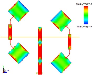
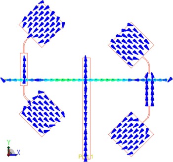
Current distribution and electric field distribution at 9.99 GHz using ADS are shown in Figs 20 and 21, respectively. The surface current distribution of the proposed array antenna is obtained using optimal design parameter values. It is seen that the electric currents are uniformly distributed but the intensities are at maximum level on side edges (left and right) of each patch element. From the figure of electric field distribution, it is found that the electric field of the patch elements in each side is orthogonal.
Current distribution of the array.

Electric field distribution of the antenna.

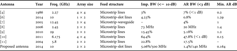
Comparison based on performance among proposed CP array antenna with other CP array antennas proposed in the recent past is tabulated in Table 2. It is seen that the designed antenna provides a good impedance bandwidth and axial ratio bandwidth with good CP quality. So the proposed antenna is a good candidate for various microwave wireless communication applications.
Optimized parameters of the proposed antenna.

Comparison.

VI. CONCLUSION
The design of a circularly polarized array antenna at 10 GHz with parametric analysis has been presented. The CP radiation of the proposed array antenna is excited using only linear polarized patches with microstrip–slot feed line network. This feed line network is realized employing both-sided MIC technology which helps to eliminate the impedance matching problem of conventional microstrip feed network. The most remarkable feature of this array antenna is that due to the simple and symmetric structure, the proposed antenna is suitable to expand array size, i.e. 4 × 4, 8 × 8, and so on. Parametric analysis has been performed to optimize the antenna for excellent performance. The return loss exhibits an impedance bandwidth of around 5% and the 3 dB axial ratio bandwidth is approximately 1.4%. The proposed array antenna radiation is LHCP with a low cross-polarization level. The good radiation performance and flat gain make the proposed planar array antenna suitable for various wireless applications such as various kinds of RF sensors, RFID systems, etc.
 Muhammad Asad Rahman was born in Chittagong, Bangladesh on October, 1986. He received his B.Sc. degree in Electrical and Electronic Engineering from Chittagong University of Engineering and Technology (CUET), Bangladesh in 2009. Currently he is pursuing M.Sc. degree on large-scale extensible microstrip array antenna and also working as a faculty member in CUET, Bangladesh. His field of interest is microstrip antenna design, polarization diversity techniques, wireless power transfer, and next generation wireless communication system. He is a student member of IEEE and member of Institute of Engineers, Bangladesh.
 Quazi Delwar Hossain (MIEEE) was born in Barisal, Bangladesh, in 1976. He received his B.Sc. degree in Electrical and Electronic Engineering from Chittagong University of Engineering and Technology (CUET), Chittagong, Bangladesh, in 2001; the M.E. degree in Semiconductor Electronics and integration sciences from Hiroshima University, Hiroshima, Japan, in 2007; and the Ph.D. degree in Microelectronics from the University of Trento, Trento, Italy, in 2010. During his Ph.D. program, he also spent a period with the SOI Group, Bruno Kessler Foundation, Trento, Italy as a Postgraduate Researcher. From 2001 to 2007, he was with CUET as a Lecturer. In 2007, he became an Assistant Professor with the Faculty of Electrical and Computer Engineering, CUET. Presently he is working as an Associate Professor at the Institution. His research interests include image sensors, antenna design and related readout circuit simulation and experimental characterization of semiconductor devices, sensors, and photovoltaic cells.
 Md. Azad Hossain (MIEEE) was born in Dhaka, Bangladesh, in 1981. He received his B.Sc. degree in Electrical and Electronic Engineering from Rajshahi University of Engineering and Technology (RUET), Rajshahi, Bangladesh, in 2004. The M.E. degree in EEE from Saga University, Saga, Japan, in 2010; and the Ph.D. degree in Science and Advanced Technology, in 2013 from the same Institute. From 2013 to 2014, he was with Chittagong University of Engineering and Technology (CUET) as a Lecturer. Presently he is working as an Assistant Professor at CUET. His research interests include Microwave antenna design and related readout circuit simulation and experimental characterization.
 Eisuke Nishiyama was born in Saga, Japan. He graduated from the Department of Electronics, Saga University, in 1987, completed the M.S. program in 1989, and became a member of the technical staff there. He was a research associate from 1997 to 2007. He has been an assistant professor since 2007. He was a visiting scholar of the UCLA from 2007 to 2008. His research interest is planar antennas, especially active antennas. He holds a Dr. Eng. degree. He was the chair of the IEEE AP-S Fukuoka Chapter from 2013 to 2014, and is a member of IEEE.
 Ichihiko Toyoda received the B.E., M.E., and the Dr. Eng. degrees in communication engineering from Osaka University, Osaka, Japan. In 1990, he joined the NTT Laboratories, Kanagawa, Japan, where he was engaged in developmental research of the 3-D MMICs, MMIC design software based on the 3-D masterslice MMIC technology, millimeter- and quasi-millimeter-wave high-speed wireless access systems, and their applications. He was also active in developing IEEE 802.11, 802.15, and other national standards. He is now a Professor at Saga University, Japan from 2011. His current interests concern microwave-circuit and antenna technologies for microwave and millimeter-wave wireless systems. Dr. Toyoda received the 1993 Young Researcher's Award, the 2004 Electronics Society Award, and 2010 Best Paper Award presented by the IEICE, Japan; the Japan Microwave Prize presented at the 1994 Asia-Pacific Microwave Conference and many NTT R&D awards. He is a senior member of IEICE and a member of IEEE.