Introduction
The fundamental materials science, chemistry, physics, and biologic properties of Ultrananocrystalline Diamond (UNCD) films are being investigated, due to potential new applications in industrial[Reference Auciello and Sumant1, Reference Fabisiak and Staryga2] and high-tech products[Reference Kraft3] and UNCD-coated industrial[Reference Suman, Krauss, Gruen, Auciello, Erdemir, Wlliams, Artiles and Adams4] and high-tech[Reference Zeng, Konicek, Moldovan, Mangolini, Jacobs, Wylie, Arumugam, Siddiqui, Carpick and Carlisle5] products already in the market. The technological applications of UNCD coatings are based on their unique combination of properties such as high wear resistance,[Reference Auciello and Sumant1, Reference Suman, Krauss, Gruen, Auciello, Erdemir, Wlliams, Artiles and Adams4] highest hardness relative to any other films,[Reference Auciello and Sumant1, Reference Suman, Krauss, Gruen, Auciello, Erdemir, Wlliams, Artiles and Adams4] lowest friction coefficient compared with metal and ceramic coatings,[Reference Auciello and Sumant1, Reference Suman, Krauss, Gruen, Auciello, Erdemir, Wlliams, Artiles and Adams4] resistance to chemical corrosion in corrosive industrial fluids[Reference Auciello and Sumant1, Reference Zeng, Konicek, Moldovan, Mangolini, Jacobs, Wylie, Arumugam, Siddiqui, Carpick and Carlisle5] and body fluids,[Reference Xiao, Wang, Carlisle, Mech, Greenberg, Freda, Humayun, Weiland and Auciello6] negative electron affinity, low work function for electron emission[Reference Auciello and Sumant1, Reference Suzuki, Ono, Sakuma and Sakai7] high electrical conductivity for N-UNCD films with nitrogen atoms incorporated in grain boundaries[Reference Auciello and Sumant1, Reference Bhattacharyya, Auciello, Birrell, Carlisle, Curtiss, Goyette, Gruen, Krauss, Schlueter, Sumant and Zapol8] high electrical conductivity for Boron-doped UNCD films, produced by inserting Boron atoms during film growth.[Reference Zeng, Konicek, Moldovan, Mangolini, Jacobs, Wylie, Arumugam, Siddiqui, Carpick and Carlisle5] Alternatively, nitrogen and Boron atoms incorporated in other nanocrystalline diamond films also exhibited high electrical conductivity.[Reference Bhattacharyya9–Reference Sun, Wang, Weng and Liu11] The electrical conductivity properties of doped diamond films are suitable to enable many applications like electrodes for electrolysis-based water purification,[Reference Zeng, Konicek, Moldovan, Mangolini, Jacobs, Wylie, Arumugam, Siddiqui, Carpick and Carlisle5] thermionic and field emission devices,[Reference Auciello and Sumant1, Reference Suzuki, Ono, Sakuma and Sakai7, Reference Kato, Takeuchi, Ogura, Yamada, Kataoka, Kimura, Sobue, Nebel, Yamasaki, Meir, Stephanos, Geballe, Mannhart, Suzuki, Ono, Sakuma, Sakai, Schwede, Bargatin, Riley, Hardin, Rosenthal, Sun, Schmitt, Pianetta, Howe, Shen, Melosh, Sun and Grilj12] and high power electronic devices.[Reference Seo, Wu, Mikael, Mi, Blanchard, Venkataramanan, Zhou, Gong and Morgan13, Reference Wort and Balmer14]
In relation to the processing to produce Boron doping of UNCD or any other diamond films, during growth, the main drawback is the Boron contamination of the chamber where the films are grown, which result in that the contaminated chamber can only be used for the growth of Boron-doped diamond films. Therefore, it is important, from the industrial process point of view, to develop alternative processes that may enable the production of Boron-doped diamond films without contaminating the expensive chambers used to grow diamond films. In this sense, thermal diffusion provides a good alternative low-cost process for producing Boron-doped diamond films. Thermal diffusion processes are commonly used for creating p-n junctions during the fabrication of Silicon-based electronic and photovoltaic devices.[Reference Auciello and Sumant1Reference Zeng, Konicek, Moldovan, Mangolini, Jacobs, Wylie, Arumugam, Siddiqui, Carpick and Carlisle5, Reference Bentzen, Schubert, Christensen, Svensson and Holt16]
Based on the information presented above, the R&D effort reported in this paper, focused on developing a thermal diffusion process for producing Boron doping of UNCD films after growth, using a dedicated oven system, with much lower cost than the cost involving Boron doping of diamond films during the growth process in a dedicated Boron contaminated system. The thermal diffusion process can potentially be used for creating p-n junctions for polycrystalline diamond film-based electronic devices.
This paper focuses on describing the results from research and development of a novel process for Boron doping large area UNCD films by thermal diffusion after growth, thus eliminating the problem of Boron contamination of the diamond film growth chamber. The research is focused on understanding the chemical, structural, and electrical properties of the UNCD films before and after doping with Boron by thermal diffusion.
Experimental methods
UNCD film growth
UNCD films were grown using the Microwave Plasma Chemical Vapor Deposition (MPCVD) technique implemented in an IPLAS (Germany, GMBH) MPCVD reactor. The UNCD films were grown on 100 mm diameter Si (100) oriented wafers coated with silicon dioxide (SiO2) layers (~300 nm thick) grown via a thermal growth process. The substrates surfaces were seeded with nanocrystalline diamond particles, via immersion of the substrates in a solution of nanocrystalline diamond particles in methanol in an ultrasonic system, which shakes the solution with ultrasonic waves that embedded the diamond nanoparticles on the surface of the substrates, providing the seed to grow the UNCD films. The UNCD films were grown via formation of a plasma, produced by coupling a microwave power of 2500 Watts on a mixture of Ar (88 sccm)/CH4 (2 sccm)/H2 (10 sccm) gases flown into the growth chamber to a total pressure of 60 mbar. The substrates were heated to ~676 °C on the surface (measured with a pyrometer focused on the substrate surface). The UNCD films were grown for 2 h, resulting in a film thickness of ~630 nm, as measured by cross-sections SEM. The as-deposited UNCD films were characterized before and after annealing, using various complementary characterizations techniques, as explained in the next section.
Boron doping of UNCD films by thermal diffusion
An ~200 nm thick Boron containing film was deposited by spin coating on the surface of UNCD films grown on SiO2 (300 nm)/Si wafers, using a commercial Spin-on-Dopant (SOD) solution (Boroflim 100®), dispersed on the substrate surface via a spinning speed of 3000 rpm and a process time of 20 s. XPS analysis was done on the SOD/UNCD film, in order to confirm that Boron atoms were present in the SOD layer (see Figure SF1 in supplementary information). Subsequently, the UNCD film with the SOD film on top was baked in an atmospheric oven at 200 °C for 20 min in order to evaporate any excess solvent from the SOD film. The diffusion process was initially carried out on three samples consisting of UNCD film (~630 nm thick) grown on a SiO2 layer (~300 nm thick), which was grown on a Si substrate. The annealing-induced process for diffusion of Boron atoms inside the UNCD films were performed in a MPTC RTP-600 Rapid Thermal Processor (RTP) in a low oxygen atmosphere at 800, 900, 1000 °C for 180 s, to determine the optimum annealing temperature to produce the maximum value of charge carrier concentration and electrical conductivity in the Boron-doped UNCD films. Several samples with UNCD films were produced to do Boron doping to achieve process reproducibility. The low oxygen atmosphere was created by purging the chamber with 15,000 sccm of N2 for 10 min in order to avoid the C-based UNCD film being etched by oxygen at the high temperatures needed for Boron diffusion. Once the purging time finalized, the N2 flow-rate was changed to 2000 sccm, and after a stabilization time of 10 s, the substrate temperature was ramped from room temperature to annealing temperature (800, 900, and 1000 °C, for three separate samples to explore the effect of annealing temperature on the B-doping process) in 10 s. After the annealing time ended (3 min), the sample was quickly cooled to room temperature in 250 s, using a N2 flow-rate of 15,000 sccm.
Once the diffusion process was over, the UNCD films were ultra-sonically cleaned with acetone, methanol, and isopropanol in order to remove any remaining SOD film from the surface of the UNCD film. The Boron-doped and as deposited UNCD films were characterized by Raman Spectroscopy (Thermo Scientific-DXR-Waltham, MA, 532 nm wavelength), x-ray diffraction (XRD) (Rigaku Ultima III-The Woodlands-Texas; Cu Kα radiation, 1.524 Å), scanning electron microscopy (SEM) (ZEISS SUPRA-40)-Thornwood-New York, Hall Effect measurement (Lake Shore 8400 Series), Secondary Ion Mass Spectrometry (SIMS) (Cameca ims-6f-Gennevilliers Cedex—France), x-ray Phototelectron Spectroscopy (XPS) (Versa Probe II- Chanhassen, MN, 20 KeV Cu source), and Ultra Violet Photoelectron Spectroscopy (UPS) (using a Versa Probe II- Chanhassen, MN, 21.2 eV He source). Raman, XRD, and SEM characterizations were done before and after the annealing process to confirm that there was no induced graphitization, damage or change in morphology or crystallinity in the films during the diffusion process. XRD, Hall effect, SIMS, XPS, and UPS characterizations were performed to confirm the insertion of Boron atoms into the film, determine the Boron atoms concentration profile from the surface into the bulk of the films, and study the changes in film chemistry, electrical properties (resistivity, charge carrier concentration and carrier mobility) and band structure (band gap, Fermi level and work function) produced during the diffusion process.
Results and discussion
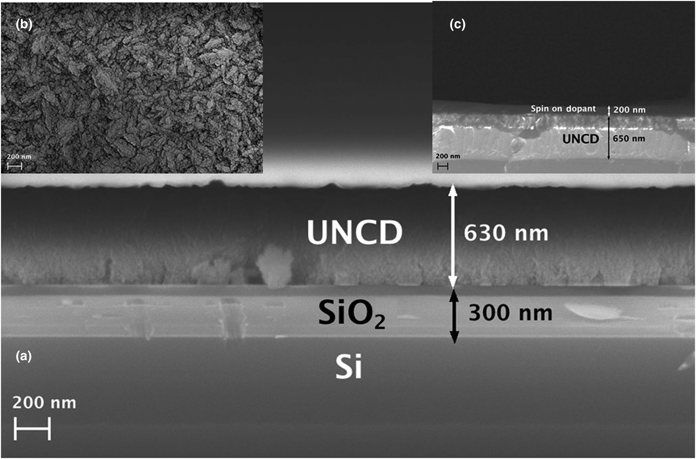
Figure 1 shows SEM cross-section (a) and top view (b) of the UNCD films as deposited, and the cross-section of the UNCD film with the SOD layer on top (c). The SEM top view image [Fig. 1(b)] shows a smooth UNCD surface with many grain agglomerates as is expected in UNCD films.[Reference Auciello and Sumant1] The SiO2, UNCD, and SOD Boron source films thicknesses were determined via cross-section SEM images (300 nm, 630 nm, and 200 nm thicknesses [Fig. 1(c)], respectively). AFM analysis was used to measure the surface roughness of the UNCD films before and after the annealing process, the latter used to insert Boron atoms inside the UNCD films. The AFM analysis showed that the UNCD surface roughness remained fairly similar before (11.3 nm rms) and after (15.9 nm rms) annealing (see Figure SF2 in supplementary information).
SEM images: (a) cross-section, (b) top view of the UNCD film as grown, (c) cross-section of the UNCD film with spin-on-dopant (SOD) film on top.

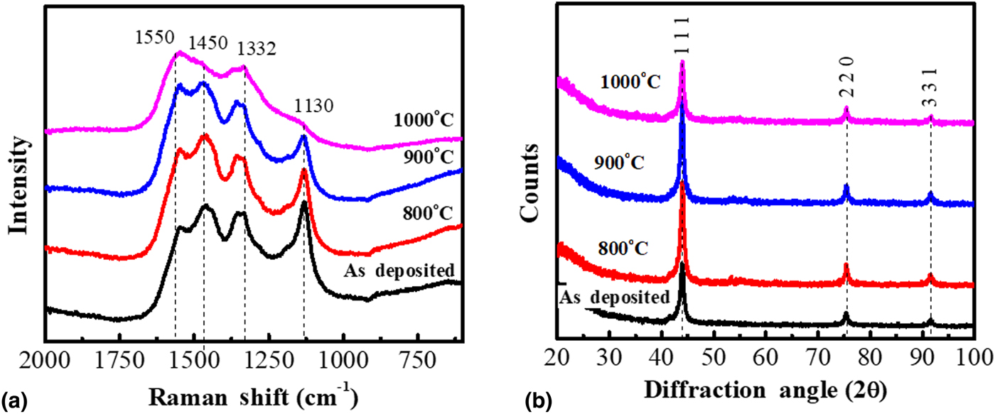
Raman analysis is a reliable quick non-destructive way to characterize diamond[Reference Filik17] Fig. 2 shows the Raman spectra (a) and XRD diffractograms (b) of UNCD films before and after Boron doping by thermal diffusion at different temperatures. The Raman spectra show the 1550 cm−1 G band attributed to sp2 carbon atoms bonds,[Reference Auciello and Sumant1, Reference Williams10, Reference Birrell, Gerbi, Auciello, Gibson, Johnson and Carlisle18] the 1350 cm−1 D band attributed to disorder-induced sp2 carbon atoms bonds,[Reference Auciello and Sumant1, Reference Williams10, Reference Birrell, Gerbi, Auciello, Gibson, Johnson and Carlisle18] the 1450 and 1130 cm−1 bands both attributed to C = C and C-H vibration modes in Transpolyacethylene (TPA) molecules, respectively.[Reference Fuentes-Fernandez, Alcantar-Peña, Lee, Boulom, Phan, Smith, Nguyen, Sahoo, Ruiz-Zepeda, Arellano-Jimenez, Gurman, Martinez-Perez, Yacaman, Katiyar and Auciello19, Reference Alcantar-Peña, Lee, Fuentes-Fernandez, Gurman, Quevedo-Lopez, Sahoo, Katiyar, Berman and Auciello20] All the Raman bands are due to chemical bonds of carbon atoms in the grain boundary network of the UNCD films. A tiny peak at 1332 cm−1, characteristic of sp3 carbon atoms bonding in diamond, can also be observed for the film annealed at 1000° C, indicating that for this annealing temperature the grain size has increased to a value corresponding to the low nanocrystalline diamond (NCD) grain size range. The Raman band at 1130 cm−1 is reduced significantly after the UNCD film Boron-induced doping annealing at 900 °C, and it almost disappears for the UNCD film annealed at 1000 °C, during Boron doping. On the other hand, the Raman band at 1450 cm−1 is halfway and significantly reduced for the UNCD film annealed at 900 and 1000 °C, respectively, during the Boron doping process. The changes observed in the Raman spectra are correlated with changes in the grain boundary structure and chemistry of the UNCD films, mostly due to loss of TPA molecules and enhancement of sp2 carbon atoms bonds for Boron atoms diffusion-induced annealing temperatures ≥900 °C.[Reference Seo, Wu, Mikael, Mi, Blanchard, Venkataramanan, Zhou, Gong and Morgan13] The changes observed in the Raman spectra correlate with desorption of hydrogen atoms from the grain boundaries, during the doping-induced annealing process, correlated with reports in the literature related to crystalline diamond annealed at high temperatures (above 800 °C) revealing hydrogen desorption from the surface.[Reference Cui, Ristein and Ley21] Visible Raman spectra of UNCD films should only show the grain boundary signals since the signal of the small UNCD grains (2–5 nm) is easily overpowered by the signal from the grain boundaries. However, the fact that a very small peak, corresponding to sp3 carbon atoms diamond bonds, is observed for the 1000 °C annealing, indicates that the grain size as grown slightly to the NCD range (~12 nm) above the typical UNCD grain sizes (3–5 nm),[Reference Fuentes-Fernandez, Alcantar-Peña, Lee, Boulom, Phan, Smith, Nguyen, Sahoo, Ruiz-Zepeda, Arellano-Jimenez, Gurman, Martinez-Perez, Yacaman, Katiyar and Auciello19, Reference Alcantar-Peña, Lee, Fuentes-Fernandez, Gurman, Quevedo-Lopez, Sahoo, Katiyar, Berman and Auciello20] for that temperature annealing. The XRD diffractograms show only peaks attributed to diamond at 43.9° (111), 75.4° (2.2.0), and 91.7° (331) planes [see Fig. 2(b)], indicating that the films have mostly sp3 carbon atoms bonds characteristic of diamond, without any graphite phase.[Reference Alcantar-Peña, Lee, Fuentes-Fernandez, Gurman, Quevedo-Lopez, Sahoo, Katiyar, Berman and Auciello20] The grain size of the films was estimated by the well known Scherrer equation using the FWHM (0.49°) of the (111) peak,[Reference Bob Downs and Bartelmehs22] which yielded an estimated grain size of about 12 nm with an error of about ±5 nm. The grain size of the diamond films determined from XRD analysis is consistent with the Raman spectra shown in Fig. 2(a), where the film annealed at 1000 °C shows a small 1332 cm−1 peak observed for NCD films, but not observed for films annealed at 800 and 900 °C, which correlates with the grain size range <10 nm, corresponding to UNCD films.[Reference Auciello and Sumant1, Reference Filik17] The XRD peaks remain very sharp [see Fig. 2(b)], with no significant change in their FWHM, after Boron doping of the UNCD films in all the annealing temperature range used, indicating that there is no induced graphitization or damage in the UNCD films during the doping process.
(a) Raman spectra, (b) XRD diffractograms of UNCD films before and after doping with Boron atoms at different annealing temperatures.

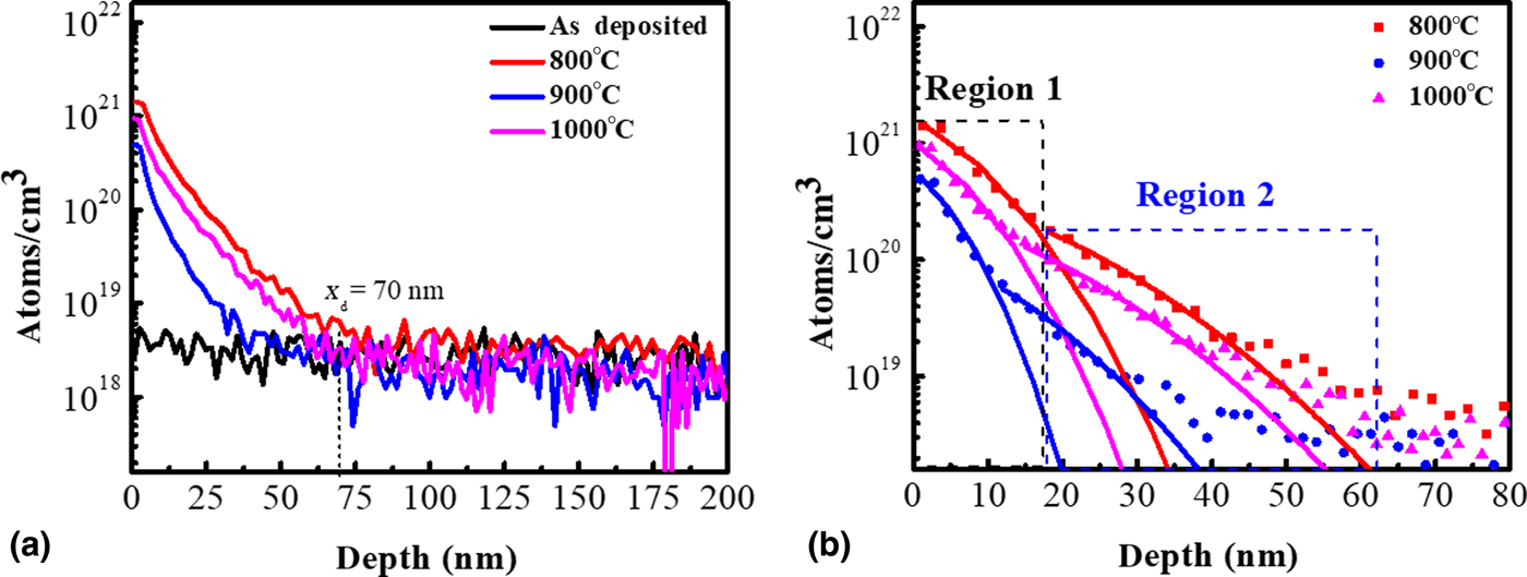
The Boron atoms depth profile observed by SIMS analysis, shown in Fig. 3(a), indicates that the concentration of Boron atoms is within the same order of magnitude, with a diffusion depth of about 70 nm and a maximum concentration of about 1021 cm−3, in the surface, for all doped films, in the temperature range used in this work, indicating a very shallow Boron atom distribution in the UNCD films.
(a) SIMS Boron atoms depth profiles of the UNCD films before and after Boron doping at the different indicated annealing temperatures. (b) SIMS Boron atoms fitted depth profiles using Fick's second law solution for the doped UNCD films.

The diffusivities of Boron atoms in UNCD films, for the diffusion temperatures used in the studies reported in this paper, were calculated by fitting the SIMS profiles to Fick's second law[Reference Tyrrell23] solution for a semi-infinite crystal with constant surface concentration:
 $$C(x,t) = C_{\rm s}erfc\left( {\displaystyle{x \over {2\sqrt {D_{\rm B}t}}}} \right)$$
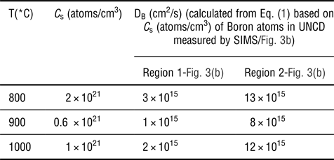
where C is the concentration of Boron atoms from the surface to a depth × into the UNCD film, C s is the concentration of Boron atoms in the surface of the film, erfc is the complementary error function, x is the film depth, D B is the diffusivity of Boron atoms in UNCD for a given temperature and t is the diffusion time. The fitted profiles of Boron atoms distribution through the UNCD films annealed at different temperatures are shown in Fig. 3(b), while the concentrations of Boron atoms on the surface and calculated diffusivities in the doped UNCD films are shown in Table I.
Diffusivities and Boron surface concentrations obtained from SIMS data after Boron-doping of UNCD films at different temperatures.

The concentrations of Boron atoms (C S) on the surface of UNCD films, measured by SIMS, were between 0.6 × 10²¹ and 2 × 1021 cm−3 for UNCD films annealed between 800 and 1000 °C [see Fig. 3(a) and Table I]. On the other hand, the diffusivities (D B) of Boron atoms inside the UNCD films, obtained from calculations using Eq. (1) with the Boron atoms depth concentration obtained from SIMS-measured Boron atoms profiles, were between 1 and 3 × 10⁻¹⁵ cm2/s for the first 20 nm of diffusion depth [region 1 in Fig. 3(b)], and between 8 and 12 × 10−15 onward (region 2) for films annealed at 800–1000 °C [Fig. 3(b)] to induce Boron atoms doping. A possible explanation for the increase in Boron atoms diffusivities for higher depths (from 20 nm onward) could be that the amount of grain boundaries in the film increases with depth facilitating the diffusion of Boron atoms. The diffusivity of B atoms in single crystal diamond reported in the literature, for an annealing temperature of ~1200 °C is around 2 × 10⁻¹⁶ cm2/s,[Reference Sung, Popovici, Prelas and Wilson24] and around 6 × 10⁻¹⁵ cm2/s for polycrystalline diamond (~10 µm grain size) at 770 °C.[Reference Popovici, Sung, Khasawinah, Prelas and Wilson25] In this work, diffusivities 1 and 2 orders of magnitude higher than single crystal diamond in the first 20 nm and at deeper depths (20 nm onward), respectively, were obtained for Boron atoms inserted in UNCD films, using much lower temperatures, indicating that the grain boundaries are facilitating the diffusion of Boron atoms as mentioned above. The diffusivities of Boron atoms in UNCD films, reported in this work, are around the same order of magnitude as the diffusivity of Boron atoms in polycrystalline diamond at 770 °C (6 × 10⁻¹⁵),[Reference Popovici, Sung, Khasawinah, Prelas and Wilson25] confirming that polycrystalline diamond films tend to show higher Boron atoms diffusivities than single crystal diamond. The effect of grain boundaries on the diffusivity of Boron atoms in UNCD films could also explain why the diffusivity did not change much with annealing temperatures in the 800–1000 °C range used in this work.
The SIMS oxygen profiles in UNCD films [see Fig. SF3(a)) in supplementary information] before and after Boron doping at different temperatures shows an oxygen concentration in the order of 1022 cm−3 in the surface of the film, due to atmospheric oxygen adsorption on the surface of the film, and an almost zero oxygen concentration after the first 10 nm depth, indicating that the N2 purge prior to the annealing process was sufficient to prevent the diffusion of oxygen atoms during the doping process for the annealing time used in this work (3 min). The SIMS hydrogen profile in the UNCD films [see Fig. SF3(b) in supplementary information] shows a concentration in the order of 1021 cm−3 for the UNCD before and after Boron doping at different temperatures despite Raman results showing hydrogen desorption from the films after doping at 1000 °C, this could be due to the fact that accurate SIMS quantification is difficult for high concentrations (>1%).[Reference Vickerman and Gilmore26]
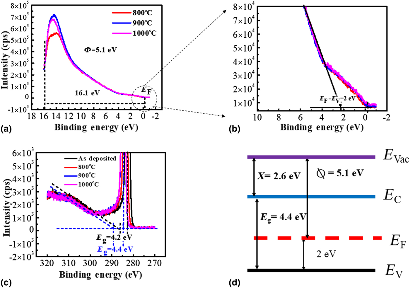
The band structures for the UNCD Boron-doped films were obtained from UPS/XPS data. The films band gap was obtained from analysis of the Plasmon XPS spectrum in the C 1s peak region [see Fig. 4(c)], using the procedure shown by Nichols et al.,[Reference Nichols, Li, Pei, Antonelli, Lin, Banna, Nishi and Shoet27] while the work function and the distance between the Fermi level and the valence band maximum was obtained from the UPS spectra [see Figs. 4(a) and 4(b)].
UPS survey spectra (a) and high-resolution spectra (b) around the Fermi Level for Boron-doped UNCD films, (c) C 1s high-resolution XPS spectra and (d) band diagram for Boron-doped UNCD films.

The calculated band gaps from the C 1s Plasmon XPS spectra were 4.2 eV for the as-deposited UNCD film, and 4.4 eV for the UNCD films after the Boron atoms-induced diffusion process during annealing in all the temperature range. It is well known that the band gap for single crystal diamond is 5.5 eV,[Reference Wort and Balmer14] indicating that the calculated band gap for the UNCD films shown in this work is an effective band gap which includes both the band gap in the grains (5.5 eV) and the band gap in the grain boundaries. UPS measurements show that the work function and Fermi level is 5.1 and 2.0 eV, respectively, for all UNCD films doped with Boron atoms in the temperature range used in this work. The Fermi level is consistent with the p-type behavior of the films. The difference between the obtained Fermi level and the acceptor level reported on the literature,[Reference Wort and Balmer14] for Boron atoms inserted in diamond (0.37 eV), could be due to grain boundary effects; further research is needed to better understand this result. A band diagram for the doped UNCD films was drawn from the information obtained in the UPS/Plasmon XPS measurements [Fig. 4(d)], in which it can be observed a p-type behavior for the UNCD films, since the Fermi level is closer to the valence band maximum than to the conduction band maximum as is expected for Boron-doped diamond.
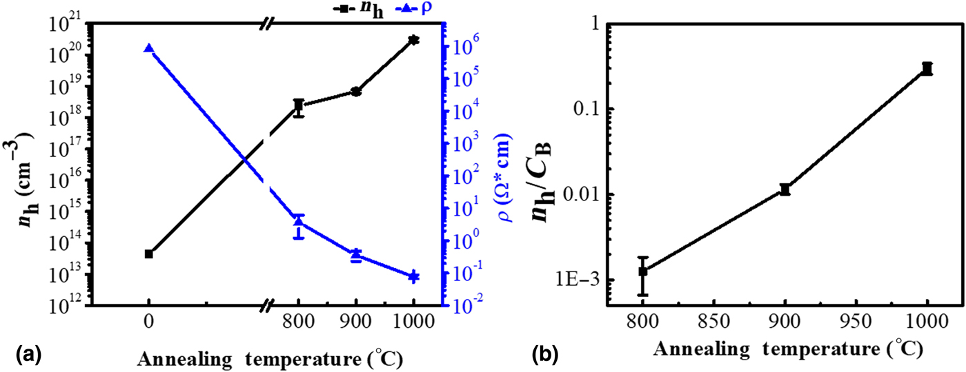
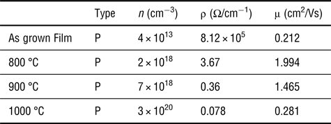
Electrical properties of the UNCD films (carrier concentration, resistivity, and carrier mobility) were investigated using Hall measurements (Fig. 5). Although the Boron atoms concentration through the UNCD films, measured by SIMS [Fig. 3(b)] are within the same order of magnitude for the doped UNCD films, Hall measurements show that the carrier concentration in the UNCD films increased by several orders of magnitude as the diffusion temperature increased, with a respective decrease in resistivity by the same orders of magnitude (Fig. 5(a)], with carrier concentrations of 4 × 10¹³, 2 × 10¹⁸, 7 × 10¹⁸, 3 × 1020 cm−3 for the as-deposited and doped UNCD films annealed at 800, 900, and 1000 °C respectively, with respective resistivities of 8.12 × 10⁵, 3.67, 0.36, 0.078 Ω/cm−1 (as shown in Table II). An explanation of this results relates to the observation that even though the Boron atoms concentration was similar in all of the Boron-doped UNCD films studied, the density of Boron atoms, activated as dopants, increased with the diffusion temperature. This is due to the fact that only impurity atoms occupying substitutional sites in the crystal lattice contribute charge carriers to the semiconductor,[Reference Pelaz28] and the probability of Boron atoms occupying substitutional sites in the UNCD film increased with temperature. A similar effect is the ratio of carrier to Boron atoms surface concentration increased exponentially with temperature, indicating that the percentage of Boron atoms occupying substitutional sites in the diamond lattice of the UNCD films grains increased with the diffusion temperature, explaining the differences in the resistivity of the films despite that the total Boron atoms concentration is similar in all the doped films. Table II also shows the semiconductor behavior and carrier mobility of the UNCD films before and after Boron doping. The semiconductor behavior was p-type for all of the UNCD films, due to hydrogen acting as an electron trap for the as-deposited film, and due to the fact that Boron atoms dopants induce p-type conduction. The carrier mobility was between 0.281 and 1.994 cm2/Vs for the UNCD films shown in this work. These values are close to the carrier mobility for UNCD films determined previously by our group (2.54 cm2/Vs),[Reference Alcantar-Peña, Lee, Fuentes-Fernandez, Gurman, Quevedo-Lopez, Sahoo, Katiyar, Berman and Auciello20] which showed a maximum carrier mobility at 900 °C. Further research is necessary to understand this behavior.
(a) Hall charge Carrier Concentration and Resistivity, (b) Ratio of Carrier concentration (nh)/Concentration of Boron atoms (CB) (measured by SIMS analysis) for the UNCD Films Before and After Doping with Boron atoms, using the new external annealing process described in this paper.

Semiconductor type, carrier mobility, carrier concentration, and resistivity for UNCD films before and after doping with Boron atoms.

Conclusions
UNCD Films were successfully doped with Boron atoms in a dedicated annealing system, using a new thermal diffusion method, after growing the films in a dedicated MPCVD system used to grow diamond films. The presence of Boron atoms in the first 70 nm of the UNCD films, from the surface into the bulk, measured by SIMS, correlates well with the increase in charge carrier concentration (from 4.37 × 10¹³ up to 2.98 × 1020 cm−3) and a correlated decrease of resistivity (from 8.12 × 10⁵ down to 0.078 Ω/cm−1), up to seven orders of magnitude with respect to the as-deposited films. In addition, a p-type semiconductor behavior for all UNCD films confirms the Boron doping of the UNCD films for each annealing temperature. The Boron atoms concentrations were within the same order of magnitude and the diffusion depth was around 70 nm for all the doped UNCD films, despite observing substantial changes (by several orders of magnitude) in Hall charge carrier concentration and resistivity with diffusion temperature, obtaining a maximum conductivity and Hall carrier concentration for the UNCD films doped at 1000 °C, indicating that the effective density of activated Boron atoms increased with temperature despite that the total Boron atoms concentration is similar for all films annealed at different temperatures. This indicates that the large grain boundary network, characteristic of UNCD films, plays a critical role in the diffusion process. The UNCD films did not suffer any graphitization nor structural damage during the diffusion process since the Raman and XRD characterizations show no signs of graphite nor changes in crystallinity. This process could in principle be extended to polycrystalline diamond films of all grain sizes, from UNCD (2–10 nm) to MCD (≥1 µm) films. The process described in this work may significantly reduce cost in the manufacture of polycrystalline diamond-based diodes, transistors, and electrodes involving Boron doping.
Supplementary material
The supplementary material for this article can be found at https://doi.org/10.1557/mrc.2018.157.
Acknowledgments
Pablo Tirado acknowledges the Consejo Nacional de Ciencia y Tecnología (CONACYT) for their financial support during this research in the group of Dr. Auciello at the University of Texas at Dallas. Prof. O. Auciello acknowledges the valuable support from the University of Texas at Dallas, through funding provided by his Distinguished Endowed Chair professor position. Dr. Yuriy Kudriavtsev (CINVESTAV-IPN) acknowledges support from CINVESTAV.