Introduction
Ultra-wideband (UWB) communication system in the wireless technology has become attractive since the Federal Communications Commission (FCC) declared a range of frequency from 3.1 to 10.6 GHz as unlicensed, in 2002 [1]. However, there are narrow band technologies (e.g. WLAN and HiperLAN) that occupy the UWB spectrum and cause interference which reduces the performance of these systems [Reference Bahadori and Rahmat-Samii2]. To improve the system performance, agile radios can be used for switchable UWB antennas with the ability to stop the single-, dual-, or multi-band interferences with band-notch characteristics. For this purpose, various techniques for designing reconfigurable band-notched UWB antennas have been presented to avoid these frequency interferences. Some techniques such as cutting slots with various shapes in the microstrip feed-line [Reference Ali, Ibrahim and Machac3], loading resonators or slots etched on the radiator [Reference Ali, Ibrahim and Machac3–Reference Nazeri, Falahati and Edwards8] or on the ground plane [Reference Nazeri, Falahati and Edwards8, Reference Liu, Xu, Wu and Liao9], loading parasitic elements with different shapes [Reference Sharbati, Rezaei and Fakharian6, Reference Badamchi and Zehforoosh10–Reference Mayuri, Rani, Subrahmanyam and Madhav12], and utilizing electromagnetic band gap and defected structures [Reference Cos, Álvarez and Las-Heras13] have been presented. With these designs, the antenna can be worked in the UWB mode when there is no coexisting system while cancelling interferences when required. In [Reference Shome, Khan and Laskar14, Reference Kumar and Kumar15], the advantages and disadvantages of different techniques and various notch antennas for application in the band-notch characteristics in the UWB systems have been verified and discussed.
To achieve the agile radios, electrical switches such as radio-frequency micro-electromechanical systems (RF-MEMS) [Reference Nikolaou, Kingsley, Ponchak, Papapolymerou and Tentzeris4], varactors [Reference Tang, Wang, Deng and Ziolkowski7] using continuously adjustable voltage sources, or PIN diodes [Reference Oraizi and Valizade Shahmirzadi11] to switch between “ON”/“OFF” states can be used in the antenna parts so as to redistribute the currents on the antenna surface and cause changes in the antenna electrical length. Among these switches, the switching times of the varactors or PIN diodes are in the range of 1–100 ns and are more compact as compared to RF-MEMS [Reference Christodoulou, Tawk, Lane and Erwin16]. Besides, biasing voltages for the varactors and RF-MEMS are very high (10–100 V) alternative to the PIN diodes (0.3–1.1 V). Since the dynamical activation, which is mainly focused in this study, relies on the voltage of bias, a proper PIN diode is applied in the form of a switching element.
Most reconfigurable band-notched UWB antennas alter their state through a decision, made by the operator. The presented UWB planar antenna with dynamical features such as switchable band-notched characteristics alters its structure based on the absence or the existence of surrounding wireless power that is wirelessly obtained by an RF harvesting unit. The proposed antenna can operate in the UWB mode, and when an ambient wireless signal at the WLAN frequency band (5.1–5.8 GHz) is received, it activates a power management unit (PMU) that deliveries the required DC power to change the state of PIN diode to “ON” state and so the antenna is converted from UWB mode into the single band-rejection mode at 5–6 GHz.
Recently, with the quick increase in RF systems, there has been important research work toward wireless energy harvesting applications in the various bands such as UHF, GSM900, GSM1800, UMTS band, Wi-Fi 2.4 GHz, LTE band 7, and so on [Reference Awais, Jin, Chattha, Jamil, He and Khawaja17]. The variation of power density (μW/cm2) in different bands depends on the time and frequency. The wireless energy harvesting by using a passive device called rectifying antenna (rectenna) is a possible solution to change the environmental wireless energy to a usable DC power efficiently [Reference Awais, Jin, Chattha, Jamil, He and Khawaja17–Reference Ogbodo, Wu, Callaghan and Wang21]. However, in most cases, the DC power is insufficient to supply an independent task. Therefore, a PMU with a DC-DC power convertor should be applied to supply the necessary DC power for the rectenna load. For the dynamically reconfigurable band-notched UWB antennas introduced in this article, the harvested wireless energy is not stored; however, it is used as an alternative for a trigger signal, empowering the PMU to supply the required DC power to the PIN diode. Moreover, to maximize sensitivity and gathered wireless energy in the rectenna, the receiving antenna should be operating in the broadband frequency and omnidirectional radiation pattern. However, due to the non-linearity behavior of the rectifier, designing a broadband rectenna is very challenging. Nevertheless, several techniques have been reported for broadband rectenna designing for both low- and high-power wireless energy harvesting [Reference Dolgov, Zane and Popovic22–Reference Reyna, Panduro and Balderas27]. So far, there is only a UWB antenna with a dynamically switchable notch-band at 5.6 GHz which is introduced in [Reference Quddious, Abbasi, Tahir, Antoniades, Vryonides and Nikolaou28]. In this work, the UWB antenna has been realized by a rectangular-shaped slot and a J-shaped stub that electrically linked to a radiating patch using a PIN diode with a complicated biasing network. Detecting a −10 dBm of an external RF signal in 5.6 GHz signal activates the dynamic making of the notch in the return loss plot which results in the elimination of the interference. While the level of received interferer signal falls below −10 dBm, the frequency notch instantly disappears, and yields to a typical UWB radiator mode. The rectenna operates at a single narrow band of 5.6 GHz that contains a patch antenna linked to a conventional voltage doubler rectifier circuit with active DC-DC booster. However, the design of a single narrow band leads to a low RF-dc conversion efficiency for low-power levels of input power density, and it is not very appropriate for wireless energy scavenging applications. A broadband rectenna design can capture more power from the existing signals of WLAN standards from RF energy sources in air and then produce more output power than a narrowband antenna. Moreover, the active DC-DC power booster needs at least a DC biasing voltage of 0.9 V and it is activated with an incident power of −11 dBm that it is not proper for actual environments. A comparison between previous work [Reference Quddious, Abbasi, Tahir, Antoniades, Vryonides and Nikolaou28] and the proposed UWB antenna with dynamically switchable band-notched characteristic in terms of different parameters is given in Table 1.
Comparison of the proposed work with previous work

In this article, a dynamically switchable single band-notched UWB planar monopole antenna with a novel whirligig-shaped radiation patch is introduced. The band-notched performance is achieved by injecting a defected ground structure (DGS) with a folded stepped impedance resonator (SIR). The equivalent filament and quasi-static equivalent circuit models of the folded DGS-SIR are investigated and extracted in our previous work [Reference Mirmosaei, Afjei, Mehrshahi and Fakharian29] to explain its performance as a band rejection structure. By inserting a PIN diode into the DGS-SIR and setting it in “ON” state, the notched band can be controlled based on an RF-activated PMU from a broadband rectenna booster system. To design a broadband rectenna, a novel wideband cypress-shaped monopole antenna as a receiving element and a broadband rectifier based on a wideband matching network [Reference Lin, Zhang, Du and Lin30] and a branch-line coupler [Reference Xiao, Du and Zhang31, Reference Zhang, Du and Xue32] are applied so that the reflected power can be returned and the RF-dc efficiency can be enhanced. The microstrip technology was applied to both the band-notched UWB antenna and the rectenna. These two were tested independently. Then, based on [Reference Olgun, Chen and Volakis33], an efficient power management system is used to design a DC-DC passive power booster for implementing an RF PMU. The combined system, fabricated as a system-on-package, can control the bias of PIN diode to switch the mode of UWB antenna, dynamically.
Switchable band-notched UWB antenna
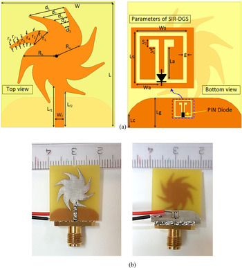
The geometry of the proposed UWB planar monopole antenna with a DGS-SIR on the ground plane as notched band configuration is shown in Fig. 1. The fabricated prototype is also illustrated in Fig. 1(b). The antenna is fabricated on a 0.8 mm-thick low-cost FR4 substrate with εr = 4.4 and tanδ = 0.02, and a compact overall dimensions of 21 (L) × 19 (W) × 0.8 mm3. The radiating structure is a novel whirligig-shaped antenna to decrease the lowest resonance frequency with increasing the antenna perimeter and get wideband operational bandwidth [Reference Ahmed and Sebak34], and it is fed by a 50 Ω microstrip transmission line. Besides that, a chambered conductor as a partial ground is applied to provide impedance matching over a wide frequency range and a radiation pattern with omnidirectional characteristics as a monopole antenna, so that the chambered edges are previously presented in [Reference Tang, Wang, Deng and Ziolkowski7, Reference Quddious, Abbasi, Tahir, Antoniades, Vryonides and Nikolaou28]. Moreover, the folded DGS-SIR contains low–high–low impedance slots, which they are inserted on the ground plane. From [Reference Mirmosaei, Afjei, Mehrshahi and Fakharian29], the resonant frequency of a half-wavelength resonator which perturbs the resonant response can be assumed as follows:


where L is the entire length of the folded DGS-SIR, c indicates the light speed in free space, and ɛeff is the effective dielectric constant of the antenna, which is assigned by ɛeff = (ɛr + 1)/2. Through the physical dimensions of DGS, the quasi-static model of an equivalent circuit of the DGS-SIR is verified in [Reference Mirmosaei, Afjei, Mehrshahi and Fakharian29]. The DGS-SIR is designed to be able to make a band-notch in the frequency band of 5–6 GHz for stopping HIPERLAN/2 (5.47–5.725 GHz) and WLAN (5.15–5.35 and 5.725–5.825 GHz). The final design parameters of the proposed UWB antenna are as follows: L = 21 mm, W = 19 mm, Lf1 = 6.6 mm, Lf2 = 6 mm, Wf = 1.5 mm, Ra = 4.3 mm, Rb = 5.5 mm, r1 = 3.1 mm, r2 = 2.5 mm, r3 = 2.1 mm, r4 = 1.25 mm, r5 = 0.85 mm, r6 = 0.72 mm, r7 = 0.54 mm, r8 = 0.35 mm, d1 = 6.1 mm, d2 = 3.7 mm, d3 = 2.1 mm, d4 = 1.2 mm, d5 = 0.6 mm, Lg = 5 mm, Lc = 2.2 mm, Ws = 2.9 mm, Ls = 2.9 mm, Wa = 1.1 mm, La = 1.85 mm, S1 = 0.35 mm, S2 = 0.45 mm, g = 0.21 mm.
(a) Configuration of the designed switchable band-notch UWB antenna. (b) The fabricated antenna prototype.

As seen in Fig. 1, the DGS-SIR is controlled by applying a PIN diode as an electronic switch to accommodate the reconfigurability. Therefore, the proposed antenna can be operating in two modes (a normal UWB mode or a single band-notched mode) depending on the PIN diode state. In the ON state of the PIN diode, the DGS-SIR acts as a resonator slot which impacts on the current flow distribution at the band-notch frequency and causes to yield band-notch characteristic. However, in the OFF state, the DGS-SIR acts as a square ring slot which lets the current to flow in the feed line and radiating patch routinely, and so lets the desired signal at 5.6 GHz to pass at the notch-band. In this work, a PIN diode by Infineon (model BAR50-02V) is selected, which is proper for WLAN bands. However, the actual PIN diode as a “switch element” has an additional parasitic effect on the performance of the antenna, which requires to be considered into simulation and account [Reference Fakharian, Rezaei and Orouji35]. Figure 2 shows the circuit model applied in the ON/OFF states in the full-wave simulation. It can be seen that the ON/OFF states have inductance L that is the packaging inductive effect. In the forward biased (ON state), the equivalent circuit has a low forward resistance RS that is the greatest limiting factor for this state and determines the insertion losses. The equivalent circuit for zero or reverse biased (OFF state) has a parallel combination of RP (reversed bias resistance) and CT (total capacitance), that gives the isolation. These parameters need to construct the model of the circuit which they are set in a datasheet of the selected PIN diode by the manufacturing company. Based on the datasheet of PIN diode [36], for the OFF state, it has a parallel circuit with a capacitance of CT = 0.15 pF and a resistance of around RP = 5 kΩ, while for the ON state, it has a forward resistance of RS = 3 Ω. For this PIN diode, the series parasitic inductance because of chip packaging is only L 1 = 0.6 nH, and so it can be ignored for the simplicity.
The PIN diode-equivalent RF circuit at the OFF and ON states.

In the proposed structure, owing to the configuration of the folded DGS-SIR, there is no need for incorporating parasitic components such as capacitors which may destroy the antenna performance; therefore, this configuration can reduce the complexity of biasing circuit. Moreover, the DC lines can be directly linked to the PIN diode on the antenna backside in the ground plane and therefore, the characteristics of the monopole antenna such as radiation do not experience any perturbation. Furthermore, an inductor could be applied in series with each DC lines to choke the RF signal in the DC lines, but since the DC voltage of biasing for PIN diode is supplied from the output of the DC-DC power convertor, which is clarified in section “DC-DC power booster”, due to the internal circuit of the power convertor, it is not essential to use RF choke.
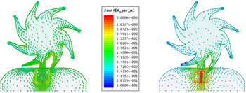
In order to better find the phenomenon behind the band-notch UWB performance, the surface current distributions at the notched frequency of 5.5 GHz for both “OFF” and “ON” states are shown in Fig. 3. It can be seen that the current is focused at the edges of the folded DGS-SIR and oppositely directed between the exterior and interior edges, while the current return path is completely disturbed and the current is limited to the margin of the DGS-SIR at 5.5 GHz in the “ON” state. As a result, the resulting radiation fields can be suppressed, and high attenuation near the resonant frequency is attained, therefore the notched band produced. By adapting the dimensions of the folded DGS-SIR, the center frequencies of the notched band can be adjusted.
The surface current distributions on the antenna at 5.5 GHz in the (a) “OFF” state and (b) “ON” state.

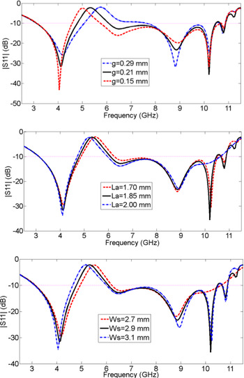
As a parametric study for finding out the performance of the resonator slot, the effects of the resonator gap (g), the arm lengths (La) and (Ws) of the DGS-SIR on the impedance matching characteristics are carried out in the OFF state in which resonator is active. Figure 4(a) shows the reflection coefficient (|S11|) at different g of the band-notched resonator. It is clear that g effects the band-notched frequency position. The center frequency position is shifted from 5 to 5.75 GHz when g is varied from 0.15 to 0.29 mm and g of 0.21 mm is selected in order to realize the favorite band-notched characteristics. The variation of the band-notched frequency position with the gap distance g is through the fact that the gap capacitance decreases, when the gap distance increases. Therefore, by increasing the gap distance, the resonant frequency increases. Figures 4(b) and 4(c) illustrate the return loss at different La and Ws, respectively. When the length of La and Ws increases, the notched band moves to the lower frequency. The changes of the resonant frequency of the DGS-SIR with the arm lengths are also because of the fact that when these parameters increase, the DGS-SIR inductance increases; therefore, the center frequency of the notched band is decreased.
Simulated |S11| characteristics of the band-notched UWB antenna in the OFF state with different values of (a) g, (b) La, and (c) Ws in the folded DGS-SIR.

In Fig. 5, measurement and simulation results for |S11| parameter of the proposed band-notched UWB antenna in the both “ON” and “OFF” states are given. In the “OFF” state of the diode, the antenna radiates as a normal UWB frequency band from 3.1 to 10.75 GHz, while in the “ON” state, a band-notch from 4.8 to 6 GHz with a center frequency of 5.35 GHz appears. The measured |S11| is corresponding with the simulated one for most of the UWB frequency range. The difference between the measurement and simulation may be produced because of the imperfect soldering of the SMA connector, the variation of the substrate permittivity, or the misalignment of the PIN diode and the current limit of the PIN diode at the ON state. In this section, for turning “ON” the PIN diode, a supplied voltage of 1.1 V [36] from a DC source is applied. While in section “Implementation of combined modules and testing”, it can be active with the existence of a wireless interfering signal at 5–6 GHz as low as −8.5 dBm detected by the rectenna.
Simulated and measured |S11| of the designed band-notched UWB antenna in the ON and OFF states.

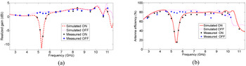
Figure 6 shows the simulated and measured values of antenna realized gain and antenna efficiency in term of the operation frequency in both states. As shown in Fig. 6(a), the average measured realized gain of the proposed antenna is nearly constant about 2 dBi over the operating band from 3 to 10 GHz, except the notched frequency bands with values equal to −8 dBi at 5.35 GHz in the “ON” state. Moreover, as shown in Fig. 6(b), the measured efficiency of the antenna is more than 75% over the desired band, except at 5.3 GHz in the “ON” state. The measured results are a little below the simulated one because of the misalignment of antenna and surrounding environment, especially in the higher bands [Reference Tang, Wang, Deng and Ziolkowski7].
Measured and simulated (a) realized gains and (b) efficiency of the proposed antenna in the OFF and ON states.

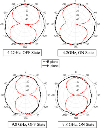
Measured radiation patterns of the proposed antenna at 4.2 and 9.8 GHz for the “ON” and “OFF” states are depicted in Fig. 7. It can be observed that the antenna provides almost bidirectional radiation pattern in the E-plane (yz-plane) and almost omnidirectional pattern in the H-plane (xz-plane) in both states, especially at lower bands. However, ripples are noted in the measured radiation patterns, because of the patch small dimension [Reference Tang, Wang, Deng and Ziolkowski7].
Measured H- and E-plane radiation patterns of the antenna at the ON and OFF state at resonant frequencies of (a) 4.2 GHz and (b) 9.8 GHz.

Broadband rectenna
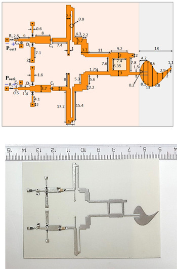
As previously mentioned, an RF harvesting system is required for the dynamic and effective PIN diode biasing in the proposed band-notched UWB antenna. For this purpose, as shown in Fig. 8, a broadband rectenna is designed and fabricated to convert 5–6 GHz RF receiving signal into a DC power. The rectenna is printed on a Rogers 4003 substrate with εr = 3.55, tanδ = 0.0027, and the overall dimension of 90 × 65 × 0.8 mm3. The designed rectenna consists of a novel cypress-shaped monopole antenna as a signal-receiving part and two sub-rectifiers which are connected to a 3 dB branch-line coupler with a grounded isolation port for increasing RF-dc conversion efficiency at the desired frequency band. Each sub-rectifier contains a network of matching, Schottky diodes SMS7630-079LF of Skyworks [37], DC pass filter, and a resistive load. Each section is connected to the next section using stubs for transferring maximum power [Reference Balanis38].
The configuration of the designed rectenna (unit: mm). (b) The fabricated rectenna prototype.

In order to realize the requirements of rectenna design, the first step is to develop and design the receiving antenna. Here, an inset microstrip-line-fed cypress-shaped monopole antenna is selected and applied which attend as a capable solution for these requirements as it is low-profile and compact size with the wideband operation and omnidirectional pattern [Reference Ahmed and Sebak34, Reference Fakharian and Rezaei39]. The inset feed method is applied, as it is easy to provide and implement a technique of impedance adjustment with a planar feed structure [Reference Wong40]. Figure 9 depicts the measured and simulated |S 11| of the receiving antenna, while the enclosure picture is independently given a fabricated antenna prototype to measure the performance of the antenna before it was linked straightforwardly to the proposed rectifier to produce the rectenna. It can be observed from the |S11| plot that the designed antenna shows a wide bandwidth of 3 GHz with a central resonant frequency of 5.4 GHz. The dimensions of the designed receiving antenna are depicted in Fig. 8.
Measured and simulated |S11| comparison of the receiving antenna. The scheme of fabricated antenna is shown in the inset photograph.

A high-performance rectifying circuit is very important in the rectenna design to get excellent power sensitivity, wideband operation, and a wide range of load with low power consumption [Reference Song, Huang, Zhou, Zhang, Yuan and Carter23]. Moreover, because of the non-linearity performance of the rectifier circuit, the rectifier input impedance differs in term of frequency, output load impedance, and also input power level [Reference Guo, Zhang and Zhu41]. Here, based on [Reference Xiao, Du and Zhang31, Reference Zhang, Du and Xue32], a proper coupler is designed and optimized that works at the working frequency and then two identical single rectifier circuits are linked to the output ports of the couplers in order to enhance the RF-dc efficiency by applying the reused reflected power in the different input power and termination load. In other words, the reflected waves from two sub-rectifiers can be partially reused by the coupler. In the configuration, as seen in Fig. 8, a wideband matching network is designed by applying an improved coupled-line using one stub with a short end before each of the branches of the divider as in [Reference Lin, Zhang, Du and Lin30, Reference Fakharian42]. The coupled line can be complicated to realize the wideband transformation of impedance. In fact, it can create a broadband impedance matching through multiple frequencies that can be adjusted for wideband performance. It is also seen in Fig. 8 that two capacitors C1, for avoiding the DC power from returning back to signal source, can be considered as a DC-block. Meanwhile, capacitors C2 are applied as DC-pass filter to store the energy of the output DC and smooth waveform before the load RL. It should be noted that in the following simulation, the model of capacitors is from MURATA and the dielectric loss of the substrate and the losses of the microstrip line are taken into account. The |S11| and RF-dc efficiency of the designed rectifier circuit are optimized using the large-signal S-parameters and the harmonic-balance simulation in Keysight–ADS for various conditions such as different frequency bands, diverse levels of input power, and a wide range of output load. The optimized parameters of the proposed rectifier circuit after optimization are shown in Fig. 8 that are the result of a gradient algorithm-based multivariable optimization.
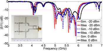
A separate fabricated rectifier circuit is given in the inset of Fig. 10 and the measured and simulated |S11| of it at three levels of input power are depicted in the same figure. A separate rectifier prototype was first constructed to measure its performance before the receiving antenna is attached. A load resistance (RL) of 2.7 KΩ is selected as an optimal termination load. It can be observed that the rectifier circuit covers the desired band for different levels of input power of interest (−20 to 0 dBm). There is a little difference between simulated and measured data due to the unknown parasitic behavior of the SMD components applied in the rectifier [Reference Song, Huang, Carter, Zhou, Joseph and Li43].
The simulated and measured |S11| of the stand-alone rectifier at three input power levels from −20 to 0 dBm at 5.6 GHz with RL = 2.7 KΩ. The fabricated prototype is shown in the inset photograph.

The RF-dc conversion efficiency of the proposed circuit rectifier can be expressed by

where, Pin is the input power, and Pdc is the output DC power. In the proposed design, the rectifier is linked straightforward to the single tone signal generator at a specific frequency in the desired band. The reason was to measure the efficiency of the proposed rectifier in term of the input power. Meanwhile, the DC voltage across RL is carried out by voltage-meter and the RF-dc conversion efficiency is given by

where Pout 1 and Pout 2 are the output power of the two sub-rectifier circuits. It is also worth stating that the two DC outputs can be linked together in parallel or in series, providing additional selections for current or output voltage. In this work, the series connection is applied for the proposed design to double the output voltage so the optimal load resistor is doubled to 5.4 kΩ.
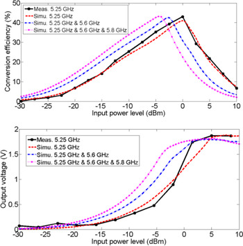
The conversion efficiency and the voltage across the termination load (RL = 2.7 kΩ) at single frequency input signal (5.25 GHz), two-tone (5.25 and 5.6 GHz), and three-tone (5.25, 5.6, and 5.8 GHz) input signals as a function of input power level are depicted in Figs 11(a) and 11(b), respectively. For single-tone input, the measured efficiency at 5.25 GHz is of around 26% and the measured output voltage is of around 0.35 V at an input power of −8.5 dBm while the maximum efficiency and voltage can reach 43% and 1.85 V with 0 dBm input power, respectively. It can be also observed that the simulated conversion efficiency and output voltage are about 33% and 0.7 V in the −10 dBm input power if the rectifier can receive the signals at the three bands simultaneously. Hence, in multi-tone cases, the efficiency and voltage improvements are about 10% and 0.35 V in the low-power levels, respectively. For the three-tone measurement, the three equal-power tones at 5.25, 5.6, and 5.8 GHz are made from three signal generators and summed up using a combiner of power, then input to the rectifier circuit. But, here there is only one single tone signal generator in the laboratory and it is not possible to test multi-tone signals, therefore just the simulated results are presented. Next, the conversion efficiency is simulated as a function of output load impedance for multiple input power levels at a single frequency and three-tone input signals, as depicted in Fig. 12. Based on the results, the rectifier works within its maximum efficiency area, in the output load of 1500–4000 Ω and it can be seen that the maximum efficiency is obtained at an optimal load of 2.7 kΩ. Since the proposed rectifier has more non-linear behavior at higher input power levels, the efficiency has dropped for higher output loads. But despite all these, the results confirm that the RF-triggered PMU efficiently works at much variable RL values for a vast range of input power which is very important in many real uses. Since the DC power and resulting voltage of rectifier circuit were not adequate to bias the applied Schottky diode, a DC-DC booster was necessary. It can be seen that the designed rectifier circuit has generally the most compact size and high voltage compared with other lately reported designs at the 5.6 GHz [Reference Quddious, Abbasi, Tahir, Antoniades, Vryonides and Nikolaou28, Reference Ou, Zheng, Andrenko, Li and Tan44]. The decrease in the conversion efficiency than [Reference Quddious, Abbasi, Tahir, Antoniades, Vryonides and Nikolaou28] is due to applying Rogers 4003 in the substrate instead of RT/Duroid 5880 which has lower quality.
The simulated and measured (a) RF-dc conversion efficiency and (b) output voltage of the proposed rectifier versus input power levels at three cases for the load resistance of 2.7 kΩ.

The simulated RF-dc conversion efficiency of the proposed rectifier versus output load at two cases for different input power levels.

DC-DC power booster
Since the rectenna output voltage is usually lower than the level of practical voltages, a PMU with a DC-DC power boost converter is typically required to use the scavenged power of the proposed rectenna. So that in accordance with the PIN diode's datasheet, at least around 1.1 V and 10 mA current (11 mW) are required to set the diode state to “ON” and effectively and dynamically change the operation mode of the UWB antenna.
Recently, the usage of a DC-DC power convertor within a rectenna has been stated in a number of published papers [Reference Zhao, Choi, Bauman, Dilli, Salter and Peckerar45–Reference Utami, Susilo and Murtianta48]. For example, in [Reference Zhao, Choi, Bauman, Dilli, Salter and Peckerar45], a DC-DC converter with switched capacitors in three stages is suggested. In [Reference Assimonis, Fusco, Georgiadis and Samaras46, Reference Song, López-Yela, Huang, Segovia-Vargas, Zhuang, Wang and Zhou47], BQ25504 as an ultra-low-power booster with a battery management is applied to charge a storage element such as a capacitor. In [Reference Utami, Susilo and Murtianta48, Reference Chen, Huang, Xing, Shi and Xiem49], 1:100 step-up transformers with LTC3108 module have proposed an RF energy harvester. On the same lines, in [Reference Olgun, Chen and Volakis33], a PMU is applied including S-882Z and AS1310 modules for regulating the output voltage and boosting the ultra-low power.
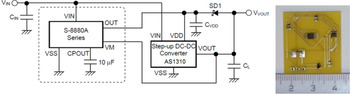
In this work, as shown in Fig. 13, a PMU based on [Reference Olgun, Chen and Volakis33] is employed in the proposed design. AS1310 is a hysteric dc-dc booster with ultralow quiescent current (<1 μA) and can be operated even when the harvested dc voltage is smaller than 0.7 V [50], while S-8880A is an efficient charge pump IC that enhances the capability of any dc-dc booster [51]. Actually, S-8880A is a new pin-compatible replacement for S-882Z compared to [Reference Olgun, Chen and Volakis33]. When a 0.35 V or higher voltage is scavenged, the circuit of oscillation inside S-8880A starts itself and generates a clock signal. Then the power activates to flow to AS1310 chip which is then transformed into a practical output DC voltage (VVOUT = 1.8 V in this study) for powering up PIN diode. Their operation is completely explained in [Reference Olgun, Chen and Volakis33]. Four 10 μF capacitors were associated in the layout to create an effective DC-DC power booster. CVDD, CIN, and CL are the capacitors as filters that bypass any noise or pulse to the ground plane. It should be distinguished that the CPOUT is a low-leakage capacitor to guarantee that sufficient energy is stored before AS1310 becomes active and feeds the PIN diode. The efficiency of the rectifier relies on the output load RL and the boost converter impedance depends on the input voltage of VIN. It must be considered that the input impedance of the DC-DC power booster differs between 3100 and 6900 Ω in the VIN variation response in the 0–1.5 V range. Therefore, according to Fig. 12, the rectifier with the booster can operate in the region of maximum efficiency. Figure 11 also depicts that the rectifier efficiency for power levels near its sensitivity (−8.5 dBm at single tone, −12 dBm at two-tone, and −14 dBm at three-tone) remains almost its maximum value.
Circuit diagram of the DC-DC power booster [Reference Olgun, Chen and Volakis33]. The fabricated prototype is also shown.

Implementation of combined modules and testing
For the implementation of the dynamically reconfigurable switchable band-notched UWB antenna using RF PMU, the PIN diodes on the back side of the switchable band-notched UWB antenna, the rectenna, and the terminals of the DC-DC power converter should be connected together using insulated wires. In such a case, the rectenna with the DC-DC power convertor works as a PMU and can be applied to enable the sending of the dc power to the PIN diode used for the dynamic reconfiguration of the proposed UWB antenna designed in section “Switchable band-notched UWB antenna”. In the earlier sections, the UWB antenna, the rectenna, and the DC-DC power convertor were discussed as separate devices independently.
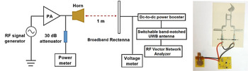
The setup of measurement was realized inside an anechoic chamber as depicted in Fig. 14. The signal is produced by an RF signal generator and amplified by a power amplifier (PA) with 37 dB gain, and transmitted using a horn standard antenna. The distance between the rectenna and the transmitting horn antenna (Gt = 12.2 dBi) is 1 m. The transmitting power to the rectenna has been measured using a power meter while the received power is accounted by using the equation of Friis transmission:

where Prec is the rectifier input RF power in dBm, Pt is the horn antenna transmitting power in dBm, Grec = 1.4 dBi is the realized peak gain of the rectenna, Gt is the realized peak gain of the horn antenna in dBi, λ is the interest wavelength, and r is the distance (r = 1 m). The output voltage of the DC-DC power booster and the rectified accessible power at the distance r, on the output load are examined by a voltage meter. During the process of measurement, it was seen that when the rectifier output voltage (which is also the enabling voltage of the DC-DC convertor) rose over 0.36 V, the convertor effectively activated the PIN diode that was employed on the switchable UWB antenna. The experiment was repeated for different levels of power at 5.25 GHz and the measurement results. This repetition continued and it is seen that the PIN diode actuation was efficient enough when the incident power Prec at the rectenna was more than −8 dBm for single-tone.
Measurement setup for dynamically reconfigurable switchable band-notched UWB antenna. The fabricated combined module is also shown.

Conclusion
In this paper, a novel UWB planar antenna using a dynamically switchable notch-band at 5–6 GHz with a broadband rectenna and a passive DC-DC convertor has been introduced and designed. The dynamic notch enables when exposed to the external single-tone RF signal ≥−8.5 dBm, while it can be active with the power levels of −12 dBm at two-tone signals and −14 dBm at three-tone signals. The UWB antenna is realized by a whirligig-shaped radiation patch and band-notched performance is obtained by etching a reconfigurable DGS-SIR on the ground plane. The PIN diode switch without any biasing network is used for electrically connecting (“ON” state) or disconnecting (“OFF” state) the resonator slot and therefore switches between the single band-rejection mode and the UWB mode, respectively. The diode biasing can occur dynamically when the interfering signal is sensed and received from a broadband rectenna that contains a cypress-shaped monopole antenna and two sub-rectifiers which are connected together with a 3 dB branch-line coupler. So the rectified 5–6 GHz RF input signal from the rectifier with a dc output voltage of 0.37 V through a 5.4 kΩ output load is used as an input voltage to a cascaded passive DC-DC converter with an output terminal linked to the PIN diode biasing and turn it to the “ON” state with a single band-notched UWB radiator mode. When the wirelessly received RF signal at 5–6 GHz is stopped, the antenna becomes a common UWB radiator mode. Therefore, the dynamically switchable UWB antenna allows the 5–6 GHz pass-band only when an RF signal in this band is not received.
Acknowledgement
The author gratefully acknowledges the experimental support provided by Sharif Center for Laboratory Services (Center Lab) at the Sharif University of Technology and Antenna Laboratory at Iran Telecommunication Research Center (ITRC). This research has also been supported by the University of Garmsar.
 Mohammad M. Fakharian was born in Tehran, Iran, in 1987. He received the B.S., M.S., and Ph.D. degrees in Electrical Engineering from Semnan University, Semnan, Iran, in 2009, 2012, and 2016, respectively. Currently, he is an assistant professor at the University of Garmsar, Garmsar, Iran. His research interests include low-profile printed and patch antennas for wireless communication, fractal, miniature, and multiband antennas, meta-materials and EBG structures interaction with antennas and RF passive components, reconfigurable antennas, RF energy harvesting, and electromagnetic theory: numerical methods and optimization techniques.