I. INTRODUCTION
The increasing demand of portable devices with wireless connectivity within a wide-frequency spectrum presents a harsh challenge for the designer of the radio frequency (RF) planar filters who has to cope with different wireless standards (GSM, UMTS, WiMAX, Wi-Fi, Bluetooth, and ZigBee). Apart from these technological issues, a tradeoff is always present between the required performance and cost, many existing microwave systems and applications have multifunction capabilities, implying that there is a demand for reconfigurable filters [Reference Hong1]. Consequently, reconfigurable filters are essential for future RF systems across commercial, defense, and civil sectors. In all these areas, reconfigurable filter technologies hold the key for controlling the spectrum of RF signals and eliminating interference and preserve the dynamic range under any signal receiving conditions. Reconfigurable filters can be realized in a variety of ways, but no matter what method of tuning is used they must conserve their transmission and reflection coefficients over the specified tuning range. Many tunable filters have been investigated in the past which control the center frequency and bandwidth [Reference Hong1–Reference Mohamed, El-Shaarawy, Abdualla and El-Henawy7]. In this paper, a novel miniaturized dual-mode resonator with reconfigurable frequency bands and ultra- wideband (UWB) filter with defected ground structure (DGS) is proposed. The characteristics of the proposed dual-mode resonators are investigated numerically and validated experimentally. This filter has the advantage of compact size, low insertion loss, sharp rejection, and high out-of-band attenuation. The filter is designed and fabricated on Rogers substrate (RO3010) with thickness of 0.635 mm, relative dielectric constant of 10.2, loss tangent = 0.0023 and the metallization thickness is 0.017 mm.
II. GEOMETRY AND CONFIGURATION OF PROPOSED RESONATOR
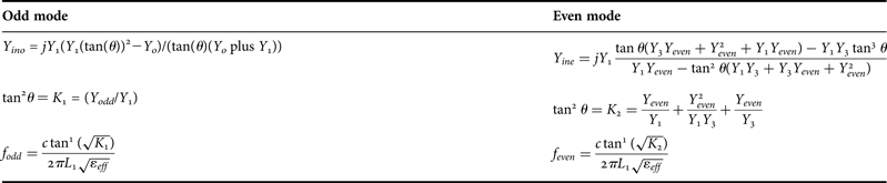
The structure of the proposed dual-mode resonator was initially analyzed in [Reference Hua, Chen and Miao6–Reference Song and Quan9], which consists of a microstrip resonator with internal-coupled lines and a quarter-wavelength open-circuited stub, as displayed in Fig. 1(a), where Y 1, θ 1, Y 3, and θ 3 denote the characteristic admittances and electric lengths of the microstrip line and open stub, respectively. Y odd, Y even, and θ 2 indicate the odd- and even-mode characteristic admittances and electrical length of the coupled lines. Since the resonator is symmetrical in structure, the resonant condition can be analyzed by the classical method of even-and odd-mode excitations as listed in Table 1. For odd-mode excitation, there is a voltage null along the symmetrical plane A–A′. The equivalent circuit is shown in Fig. 1. Taking θ 1 = θ 2 = θ 3 = θ for convenience, we can derive the input impedance (admittance) [Reference Zhang and Chen5]. The coupling structure makes it possible for the filter to generate one finite transmission zero at the lower or upper notchbands Fig. 1(b), shows the resonance frequencies of the degenerate modes. The horizontal axis is the Y3, when varied from 0.02 to 0.075S, the resonance frequency of the even mode decreases almost linearly from 2.5 to 1.4 GHz, whereas the resonance frequency of the odd mode is almost constant (about 1.83 GHz).
(a) Structure of the proposed dual-mode stub-loaded resonator and (b) simulated resonance frequencies of the degenerate modes and transmission-zero frequency against the different values of Y3.

Resonant conditions of the even- and odd-mode excitations [Reference Mohamed, El-Shaarawy, Abdualla and El-Henawy7].
As a result, the fundamental even-mode resonant frequency of the proposed resonator can be flexibly controlled, whereas the fundamental odd-mode resonant frequency is unaffected. By etching the rectangular slot as shown in Fig. 2 in the open stubs, this aperture tends to decrease the quality factor of filter, thus increasing the bandwidth [Reference Matsuo, Yabuki and Makimoto8–Reference Apisak, Kunthphong and Wanlop10].
Simulated current distributions for the two modes of the proposed resonator: (a) odd mode and (b) even mode.
Coupling coefficient of a resonator plays a key role in determining the bandwidth of a filter [Reference Pozar11]. A full-wave electromagnetic (EM) eigenmode simulator CST 2011 is used to characterize the current patterns for the resonator.
Figures 2(a) and 2(b) show the current patterns of the resulting two fundamental eigenmodes. At the fundamental odd-mode resonant frequency, there is no current flowing on the open-circuited stub, and the open-circuited stub does not perturb the fundamental resonant current distribution as shown in Fig. 2(a). On the other hand, at the fundamental even-mode resonant frequency, there is current flowing on the open-circuited stub, which changes the current distribution path, thus changing the resonant frequency as shown in Fig. 2(b). The normalized element values of the Chebyshev low-pass filter prototype with 0.01 dB ripple can be obtained from [Reference Apisak, Kunthphong and Wanlop10] as, g0 = 1, g1 = 0.4488, g2 = 0.4077, and g3 = 1.1007 that improve the passband and out-of-band performances [Reference Matsuo, Yabuki and Makimoto8]. The initial dimensions can be chosen using the above design procedure and then the CST 2011 software is used to optimize the dimensions for 1.83 GHz GSM applications, where c is the speed of light in free space, L1 is the length of the microstrip line, and ε eff denotes the effective dielectric constant of the substrate.
III. DUAL-MODE BANDPASS FILTER (BPF)
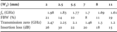
The line width for the microstrip line was chosen to give the characteristic impedance of 50 Ω and each of coupled line length and open stub is a quarter of wavelength at the mid-frequency 1.83 GHz of GSM applications of the symmetrical structure as shown in Fig. 3(a). In addition, the impacts of some parameters on frequency characteristics are analyzed in detail as shown in Figs 3(b) and 3(c). As a result, the fundamental even-mode resonant frequency of the proposed resonator can be flexibly controlled, whereas the fundamental odd-mode resonant frequency is unaffected. Besides, it can be seen from Fig. 3(b) that there is a transmission zero inherently through the notchband, and the transmission-zero frequency of the resonator can also be tuned by varying the value of Y3 [Reference Zhang and Chen5]. As Y3 increases, the transmission zero shifts from the upper to the lower notchband. This unique property allows an easy design of asymmetric responses with improved selectivity below or above the passband, by just varying the width of the open-circuited stub (W 3) as listed in Table 2.
The geometric description of the BPF (all dimensions in mm). (a) Frequency response simulation of the open-circuited stub W 3, (b) S 21 and (c) S 11.
Influence of varying open stub width (W 3) in Fig. 3.
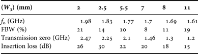
We can predict and obtain the transmission zero from the analysis of the transmission coefficient S21 [Reference Song and Quan9]. The simulated return loss of the filter is 0.97 dB and the insertion loss is 26 dB when W 3 = 2 mm, whereas the insertion loss and return loss are 30 dB and 0.17, respectively when W 3 = 2.5 mm. It should be noted that for W 3 = 2.5 mm, the response exhibits a transmission zero located close to 2.25 GHz and a FBW of 0.27 GHz (14.5%) is obtained.
IV. RECONFIGURABLE DUAL-BPF TO BANDNOTCH FILTER
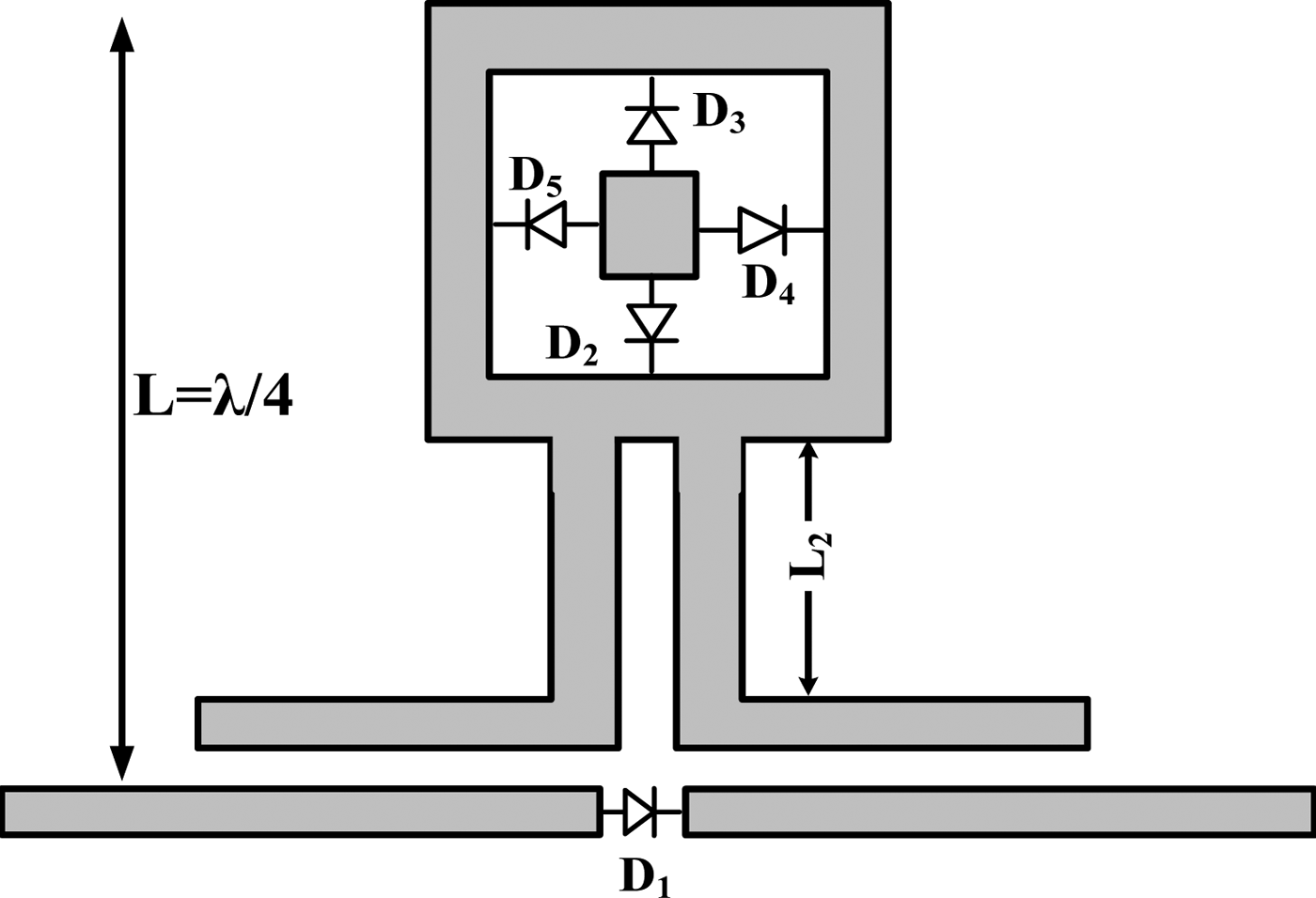
Figure 4 shows many cases for the filter according to the diodes' states. When all diodes are in OFF state, we obtain a BPF as shown in Fig. 5(a) centered at 1.83 GHz with a fractional bandwidth of 14.8%. When the diode D1 is in ON state and the other diodes are in OFF states, the filter will be bandnotched as shown in Fig. 5(b). This happens due to the fact that the open-circuited stubs may be approximated as series LC resonators when the length is near 90° [Reference Apisak, Kunthphong and Wanlop10]. When D1 and D2 are in ON state, whereas other diodes are in OFF state, one obtains a bandnotched filter with f 0 = 1.95 GHz. Other cases are mentioned in Table 3.
The reconfigurable bandpass/bandnotch (single notch) using RF PIN diode switches.
CST EM-simulated and measured S-parameter of reconfigurable frequency response of a matched BPF (a) all switches are OFF state. (b) D1 switch is ON.
The optimum states of the RF PIN diode for proposed BSF.
This filter implementation is based on the generalized coupled resonator model where the even–odd mode admittances are introduced in [Reference Pozar11]. In the case of all the PIN diodes HPND 4005 [12] is turned OFF, then the filter produces a matched bandpass at the center frequency of 1.83 GHz, the fractional band width is 14.8%, while the insertion loss at the center of the pass band is 0.93 dB. Selectivity is about 50 dB from 1.958 to 2.37 GHz at the higher frequency edge between the passband and the notch band. The operation of the reconfigurable filter between bandpass and bandnotch is based on the PIN diode D1 ON and OFF states. A photograph for the fabricated filters is shown in Fig. 6.
Photograph of the reconfigurable BPF to BSF.
However, other modifications were carried out using our proposed PIN diode model to optimize the filter performance, and then an EM simulator was used to verify and fine tune the filter performance. In principle, if switches are used on the slots of the filter instead of the short-circuit bridges in slots as shown in Fig. 4, it is expected that the center frequency of the bandnotch filter can be adjusted by activating the switches between their ON and OFF states. The short-circuit bridge is a metallic strip that makes short circuit to resemble the ON state of the diode. In addition, increased flexibility in the tuning range of the filter is by an appropriate combination of the ON/OFF states of the switches of D1, D2, D3, D4, and D5 as shown in Table 3.
We can change the center of notched band by controlling the PIN diodes states as ON/OFF as listed in Table 3. From Fig. 7, the bandnotch filter frequency shifts to 1.95 GHz (UMTS) when only the first array of switches is turned ON (state 1) and goes to 1.88 GHz (PCS) when only the second array of switches is activated (state 2). A center frequency of 1.83 GHz (GSM) is obtained when the switches are turned ON (state 3). The experimental results show a broad tuning range of 1.77 GHz with a low insertion loss of 0.6 dB. It can be seen that there is a minor distortion of the frequency response of state 2. This can perhaps be attributed to the fact that all of the switches may not have identical operating performances, which slightly degrades the overall performance of the tunable filter. One can notice that there is a resonance that takes place close to 1.5 GHz. It should be noted that this is the same as what happens as shown in Fig.15 in [Reference Hesham, Heba, Abdallah and Hadi4]. This may be attributed to the stray capacitance and inductance when introducing the RF PIN diode (ON state). This justification is assumed to the fact that when removing the diode, this resonance disappears. This work demonstrates a filter that can be switched between many commonly prescribed narrowband filter functions.
Reconfigurable bandnotch filter using RF PIN diode switches: (a) S 11 and (b) S 21.
V. RECONFIGURABLE DUAL-BAND BANDNOTCH FILTER
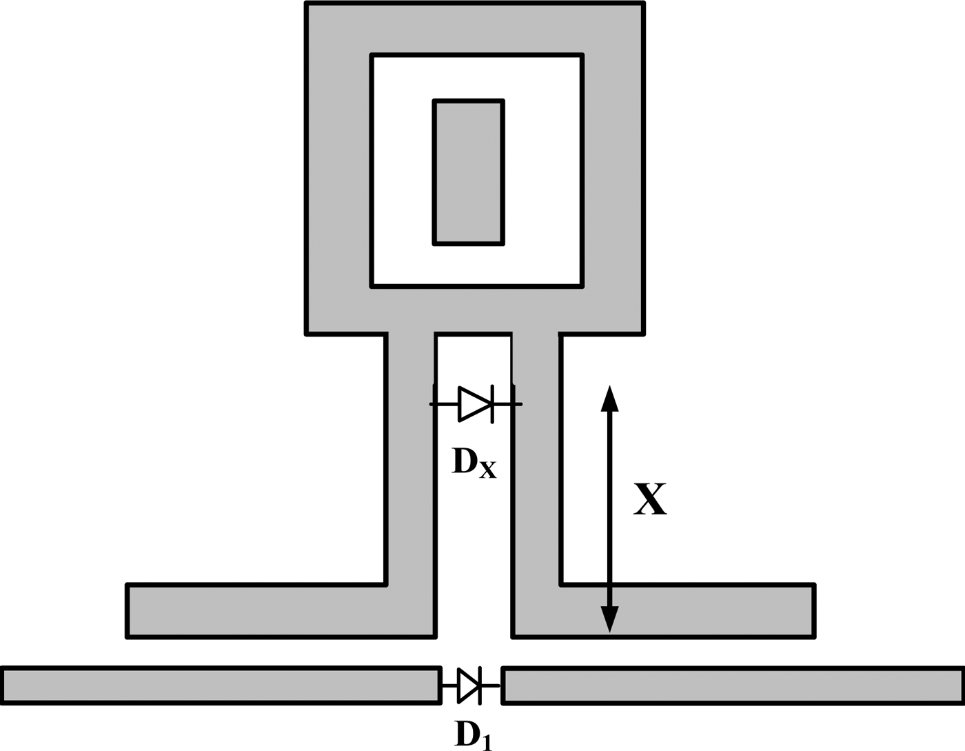
One way to have a dual-band frequency response in which bandnotch filters can be added to have a mode of operation that allows all frequencies to pass except two notched frequencies. This concept is shown in Fig. 8. Bandnotch filters with this capability are shown when all the RF PIN diodes are operating in the ON state. However, the filter in this case is matched to dual-notched band and also used as a switch in order to tune the selectively of the second notched band by changing the location of the RF PIN diode.
The tunable bandnotch filter using RF PIN diode switches.
From Fig. 9 it is seen that the center frequencies of the second notched band have the values of 2.33, 2.27, 2.22, 2.16, 2.1, and 2 GHz, or decreases by 16, 14, 11, 8.5, 5.5, and 2.5%, respectively, with reference of 1.77 GHz, when inserting the RF PIN diode at location values of 1, 1.5, 2, 2.5, 3, 3.5, and 4 mm. This means that the resonant frequency reduces by 16% by increasing the location of RF PIN diode from 1 to 4 mm, with the same compact size.
Simulated S-parameters of the reconfigurable double-notch filter: (a) S 21 and (b) S 11.
VI. UWB BPF DESIGN USING DGS AND RECONFIGURABLE FREQUENCY BAND
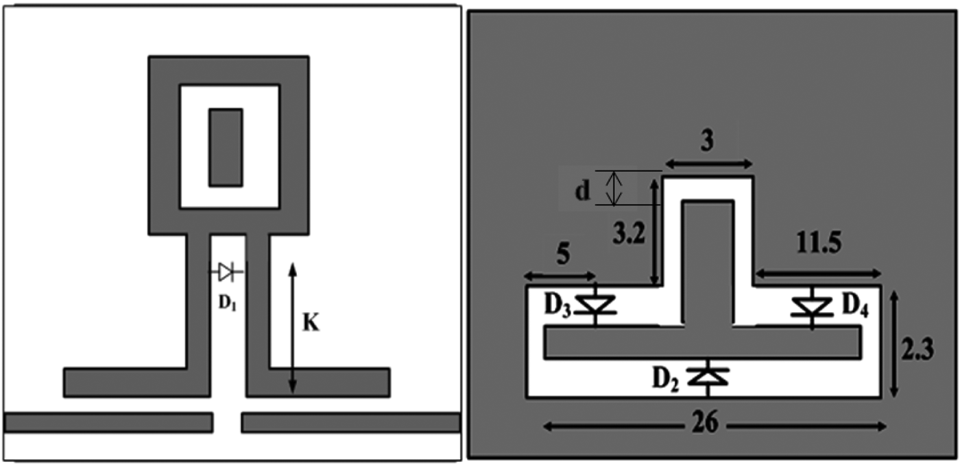
For the above BPFs, which have one transmission zero, a low sharpness factor is achieved and its bandwidth is limited to 14.5%, which is suitable only for moderate-band applications. To overcome this limitation, a DGS has been proposed and implemented in the fabrication. One remarkable advantage of using the DGS under the microstrip line is that it is possible to increase the characteristic impedance by additional effective inductance generated by the DGS [Reference Hesham, Heba, Abdallah and Hadi4], and suppression of the second harmonic using either DGS or fractal shapes [Reference Apisak, Kunthphong and Wanlop10]. The broadened width of the DGS microstrip line can be understood as the increased equivalent capacitance, which plays a great role in raising the phase constant [Reference Hesham, Heba, Abdallah and Hadi4]. UWB transmission systems are characterized using an instantaneous bandwidth greater than 0.5 GHz or a fractional bandwidth of more than 20%. In Fig. 10, we presented a novel DGS. To illustrate the UWB operation a parametric study was carried out by varying the distance (d). It was found that the even-mode frequency is adjusted by the length d = 0.7 mm.
Configuration of the microstrip UWB BPF (all dimensions in mm).
As discussed above, two transmission zeros resulting from the dual-mode resonator and the DGS coupling line can be found, as shown in Fig. 10. DGS microstrip line is used to diminish the higher order harmonics over the symmetrical shaped DGS at 2f o, of 3.8 GHz. Under the considerations of compact size, sharp rejection band and high performance are obtained by this novel BPF and designed by the DGS geometries. Simulated and measured results are shown in Fig. 11(a). It shows that the measured results matched closely with the simulated one, the results show that the proposed BPF has high performances such as achieving a 3 dB bandwidth, which extends from 1.84 to 3.43 GHz (FBW 63%), insertion loss of −0.25 dB and great sharpness about 55 dB from 1.7982 to 1.8466 GHz in low-frequency edge, and about 33 dB from 3.4329 to 3.4995 GHz in high-frequency edge.
UWB BPF using DGS: (a) simulated and measured S-parameters and (b) S-parameters when D1 is ON.
UWB BPF has three transmission poles in the passband and two transmission zeros, respectively, in the lower and upper notchbands to enhance selectivity. The experimental results show excellent agreement with the theoretical simulation results and measurements were done using an Agilent 7819ES Network Analyzer with range 0.05 to 13.5 GHz.
The reconfigurable filter can be realized using a RF PIN diode HBND 4005 [12]. In comparison to tunability of center frequency, there has been very little effort made in the tunability of bandwidth. A reason for this is the lack of methods in order to vary the perturbations of fields in DGS electronically, which is essential for bandwidth control. After a preliminary optimization, we considered the configuration shown in Fig. 10(b), in which three RF PIN diodes are able to guarantee a proper bandwidth of the operating frequency. The positions of the RF switches have been chosen by inspecting the paths of the current on the ground surface to define the most suitable place of the diodes to guarantee the current flow. This electronically reconfigurable filter mainly RF PIN diodes (D2, D3, and D4) in ON and OFF states are shown in Fig. 10(b). As it is known, any defect etched in the ground plane of the microstrip line disturbs its current distribution.
This will increase the effective capacitance and inductance. Hence, by switching the PIN diodes in DGS ON and OFF or altering the overall impedance of the filter changes the passband width. The simulated results with reconfigurable bandwidth is 18% at center frequency 1.77 GHz for ON state, which achieves a passband reconfiguration ratio greater than 4:1 as shown in Fig. 11(b).
To allow this structure to generate a narrow notched band inside the UWB as shown in Fig. 10(a), we inserted an RF PIN diode (D1) in internal coupled lines at distance (K) to change the length to generate tuned notched bands to avoid interference with UMTS at 2.1 GHz as shown in Fig. 12(a). Figure 12(b) illustrates the fabricated filter with bias lines for the HPND 4005 PIN diodes. The simulated performance results of the filter are summarized in Table 4. The group delay of the filter has been measured comparing it with the simulation, resulting in slight variation between 2 and 3 ns in the passband as shown in Fig. 13.
(a) S-parameters results for the narrow BPF at (D2, D3, and D4) ON state and (b) fabricated reconfigurable filter with DGS and RF PIN diode.
Simulated and measured of group delay at ON state at K = 2.5.
Observed results from the reconfigurable filter in Fig. 10.
VII. RESULTS AND DISCUSSION
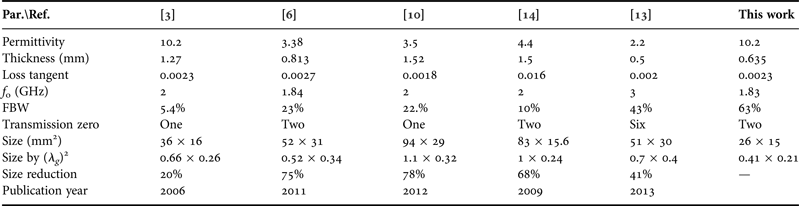
The overall volume of the filter is 26 mm × 15 mm × 0.635 mm, and the efficient electric size of the proposed filter is 0.41λ g times 0.24λ gwith size reduction of 20 [Reference Zhang and Chen3], 75 [Reference Hua, Chen and Miao6], 78 [Reference Apisak, Kunthphong and Wanlop10], 68 [12], and 41% [Reference Xue, Feng and Che13]. The fractional bandwidth of the UWB BPF is about 63%. The performance of the proposed filter along with the parameters of other BPFs in published literatures is compared in Table 5.
Comparison among various UWB BPFs.
VIII. CONCLUSION
In this paper, a dual-mode stub-loaded resonator with internal coupled lines is proposed. The performance of the resonator has been obtained by theoretical analysis and thereafter verified by simulation and experiment. The proposed resonator possesses the merit that its fundamental even-mode resonant frequency can be flexibly controlled, while the fundamental odd-mode resonant frequency remains unaffected. A novel switchable filter from BPF to BSF using an RF PIN diode with single notch and double notches is presented. Compactness as compared to the other works is achieved. By adding the DGS to the filter, the FBW rises from 14 to 63%. The sharpness increased from 45 dB (from 1.436 to 1.58 GHz) to 55 dB (from 1.7982 to 1.8466 GHz) in low-frequency edge, and about 20 dB (form 1.793 to 2.535 GHz) to 33 dB (from 3.4329 to 3.4995 GHz) in high-frequency edge. However, there is an increasing demand for reconfigurable UWB filters with/without a notchband and high selectivity for wideband communications, radar and electronic warfare systems for processing signals involving large information with high data rate. Finally, the results indicate that the proposed filters have properties of compact and miniature sizes, low passband insertion losses and high-frequency selectivity.
 Hesham A. Mohamed received his B.Sc. degree in Electronics and Communication Engineering from the University of Menofia in 2003 and received his M.Sc. degree from the Ain Shams University in 2009. He did his M.Sc. in Miniaturization Techniques for Microstrip Filters. He is currently working toward Ph.D. degree in design and implementation of compact and reconfigurable planar filters at the Ain Shams University. His research interests include design and analysis of microstrip filters, microstrip antennas, and its application in wireless communication. He now holds an Assistant Research fellowship at the Electronics Research Institute (ERI), Giza, Egypt.
 Heba B. El-Shaarawy was born in Cairo, Egypt, in 1981. She graduated from the Electronics and Communication Department, Faculty of Engineering, Cairo University, Egypt in 2003 with honors, and worked as a Teaching Assistant in the same department. She obtained her master's degree in 2005 from the Electronics and Communications Department, Cairo University, in miniaturization of microstrip filters, and Ph.D. degree from the University of Toulouse, Toulouse, France. Her fields of interest are microstrip components and antennas, electromagnetic bandgap structures, and defected ground structures.
Esmat A. Abdallah graduated from the Faculty of Engineering in 1968 and received her M.Sc. and Ph.D. degrees from Cairo University, Giza, Egypt, in 1972 and 1975, respectively. She was nominated as Assistant Professor, Associate Professor, and Professor in 1975, 1980, and 1985, respectively. In 1989, she was appointed as the President of the Electronics Research Institute ERI, Cairo, Egypt, a position she held for about 10 years. She became the Head of the Microstrip Department, ERI, from 1999 to 2006. Currently, she is working with the Microstrip Department, Electronics Research Institute, Cairo, Egypt. She has focused her research on microwave circuit designs, planar antenna systems and non-reciprocal ferrite devices, and recently on EBG structures, UWB components and antenna and RFID systems. She is a single author and a coauthor for more than 160 research papers in highly cited international journals and in proceedings of international conferences in her field.
 Hadia M. El Hennawy received her B.Sc. and M.Sc. degrees from the Ain Shams University, Cairo, Egypt, in 1972 and 1976, respectively, and the Ph.D. degree from the Technische Universitat Braunschweig, Germany, in 1982. In 1982, she returned to Egypt and joined the Electronics and Communications Engineering Department, Ain Shams University, as an Assistant Professor. She was nominated as an Associate Professor in 1987 and then a Professor in 1992. In 2004, she was appointed as the Vice-Dean for graduate studies and research. In 2005, she was appointed as the Dean of the Faculty of Engineering, Ain Shams University. She has focused her research on microwave circuit design, antennas, microwave communication, and recently wireless communication. She has been the Head of the Microwave Research Laboratory since 1982. She has published more than 100 journal and conference papers and supervised over 50 Ph.D. and M.Sc. students. Professor El Hennawy was the Editor-in-Chief of the Scientific Bulletin of the Faculty of Engineering, Ain Shams University, from August 2004 to August 2005 and is a member of the Industrial Communication Committee in the National Telecommunication Regulatory Authority (NTRA), Educational Engineering Committee in the Ministry of Higher Education, and Space Technology Committee in the Academy of Scientific Research.