Introduction
Conductive inks based on highly concentrated metal nanoparticle dispersions are important materials in the fabrication of printed electronic devices such as organic light-emitting diodes (OLEDs) and organic photovoltaic (OPV) cells.[ Reference Kamyshny, Steinke and Magdassi 1 , Reference Habas, Platt, van Heest and Ginley 2 ] Their primary purpose is the production of highly conductive, patterned metal structures that serve as shunting lines or current collecting grids in order to reduce resistive losses in the transparent electrodes.[ Reference Harkema, Mennema, Barink, Rooms, Wilson, van Mol and Bollen 3 – Reference Galagan, Zimmermann, Coenen, Jorgensen, Tanenbaum, Krebs, Gorter, Sabik, Slooff, Veenstra, Kroon and Andriessen 5 ] When applied to flexible plastic substrates, these materials allow fast high-volume production techniques to be applied, such as roll-to-roll manufacturing.[ Reference Krebs 6 , Reference Manceau, Angmo, Jorgensen and Krebs 7 ]
Since the conductivities of the as-deposited nanoparticle inks are generally poor, a post-deposition treatment is needed to enhance them, which is generally achieved by applying heat, usually in a hot air oven,[ Reference Krebs 6 , Reference Manceau, Angmo, Jorgensen and Krebs 7 ] but IR irradiation has been used as well.[ Reference Denneulin, Blayo, Neuman and Bras 8 ]
Since, however, the commonly used inexpensive polymer foils (e.g., PET (poly(ethylene terephthalate)) or PEN (poly(ethylene naphthalate)) lose their dimensional stability well below 150 °C (glass temperatures 100–105 °C (PET) and 125–130 °C (PEN); cf. Supplementary Information), thermal sintering is limited to rather low temperatures. As a consequence, relatively long sintering times are needed to achieve a reasonable functional performance.[ Reference Krebs 6 – Reference Denneulin, Blayo, Neuman and Bras 8 ] Alternatively, (near) room temperature sintering methods have been developed that achieve the formation of conductive structures by chemical rather than thermal processes. The most important examples are plasma sintering,[ Reference Reinhold, Hendriks, Eckardt, Kranenburg, Perelaer, Baumann and Schubert 9 ] which, however, is generally rather slow, and chemical sintering,[ Reference Wakuda, Hatamura and Suganuma 10 – Reference Grouchko, Kamyshny, Mihailescu, Anghel and Magdassi 13 ] which often involves wet chemical steps or exposure to vapors.
Direct selective heating of the printed metal ink is expected to allow higher process temperatures, and therefore better sintering performance in shorter time, since the polymeric foil is only heated indirectly and locally. Several methods have been evaluated in the past for high-speed sintering on plastic substrates. These methods include microwave,[ Reference Perelaer, de Gans and Schubert 14 – Reference Allen, Alastalo, Suhonen, Mattila, Leppäniemi and Seppä 16 ] electrical,[ Reference Allen, Aronniemi, Mattila, Alastalo, Ojanperä, Suhonen and Seppä 17 ] and laser sintering.[ Reference Chiolerio, Maccioni, Martino, Cotto, Pandolfi, Rivolo, Ferrero and Scaltrito 18 – Reference Yoon, Yi, Yim, Lee, Rozgonyi and Joo 20 ] One of the most promising methods is based on photonic flash sintering,[ Reference Marjanovic, Hammerschmidt, Perelaer, Farnsworth, Rawson, Kus, Yenel, Tilki, Schubert and Baumann 21 – Reference Han, Hong, Kim and Song 24 ] which recently has also been demonstrated in a roll-to-roll fabrication setup.[ Reference Hösel and Krebs 25 ] The papers published on this topic until now have concentrated on the technology's ability to achieve the desired final materials properties in short times. For process optimization to be carried out in a systematic manner, however, much more detailed insight into the photonic sintering process is required, which is currently lacking.
In this paper, we study the fast and efficient processing of conductive inks by a photonic sintering method, based on pulsed light focused in a narrow line. The basic mechanism of the technology is introduced, the sintering process is investigated and the influence of several parameters, like pulse power and pulse frequency, on the process and the final materials properties is discussed. Furthermore, a method is presented which allows monitoring in real time both electrical resistance and temperature of a printed ink line during the exposure to flashed light. This enables a more purposeful approach to optimize the photonic sintering conditions than has hitherto been possible.
Equipment and experimental results
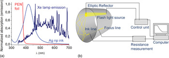
The basic principle of photonic sintering is the selective heating via light absorption. With only a few exceptions, the foils commonly used for plastic electronic applications are transparent to visible light. In contrast, metal nanoparticles frequently show strong absorption bands in this range of the electromagnetic spectrum due to surface plasmon resonance phenomena. By matching the emission spectrum of the light source with the absorption spectrum of the conductive ink, light is mainly absorbed by the ink and consequently, heat is only generated exactly at the place where it is needed. This principle is demonstrated in Fig. 1(a), where there is only very little spectral overlap between the absorption of the PEN foil used in this study and the emission of the xenon flash lamp. In contrast, the absorption spectrum of the conductive silver nanoparticle ink overlaps considerably with the lamp emission.
Working principle of the photonic sintering process. (a) Absorption spectra of PEN foil and silver nanoparticle ink, and emission spectrum of the Xe flash lamp, indicating preferential absorption of light by the ink. (b) Schematic representation of the experimental setup.

For a fast sintering process, high photonic energy densities are necessary. Achieving those without the need for enormously strong and power-consuming light sources requires focusing of the emitted radiation into a very narrow area. One possibility to realize this is by employing a cylindrical reflector with an elliptical cross section. In such a curved mirror all rays emitted by a light source placed in one focus line will be reflected and concentrated into the second focus line. By placing a sample of printed, but uncured ink there, it will be exposed to light of high intensity and is expected to quickly heat up to temperatures at which sintering will take place at a high speed. When the light is provided in short pulses, also heating of the supporting substrate can be limited by controlling parameters like pulse intensity, pulse length, and flashing frequency.
Based on this principle, a test setup was developed for studying the photonic sintering process of conductive inks [Fig. 1(b)]. It consists of a xenon stroboscope lamp placed in one of the two focus lines of an elliptical reflector. The details of the construction are revealed in the Supplementary Information. In this way, very high photonic energy densities can be achieved locally, despite the use of a simple light source with a rather moderate power output (1000 W). A four-point resistance measurement template was designed to monitor the resistance of the ink line during illumination. The sintering parameters like pulse power and flashing frequency can be controlled by a specifically designed operating software and are constantly measured by a photodiode located inside the reflector. Except for single pulses with a constant flashing frequency, the software also allows to supply the energy in short bursts of up to 32 pulses, which alternate with longer cooling breaks. The pulse length in our system varies between 3 and 8 ms, depending on the used intensity (Fig. S2).
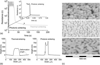
The experimental setup allowed us to monitor the electrical resistance of a printed test line of a silver nanoparticle-based inkjet ink during exposure to the flash light. For comparison, the thermal sintering behavior could also be followed in time by placing the measurement setup in a hot air furnace at predefined temperatures (typically 130 °C). All experiments described in this publication were carried out using a commercially available conductive inkjet ink. It consists of a dispersion of silver nanoparticles (diameter 30–50 nm) stabilized with a polymer shell in a mixture of ethanol, ethylene glycol, and glycerol. The silver content is 20% by weight (cf. Supplementary Information for details of composition and inkjet printing parameters). Single-layer inkjet printed lines of 25 mm length and 500 μm width have been used for the experiments described here, unless otherwise indicated. As can be seen in Fig. 2(a), conventional oven sintering at 130 °C takes about 25 s to achieve a resistance low enough to be measured, which then decreases within 10 more seconds by several orders of magnitude. However, from that time on, the further improvement is very slow, stabilizing at a value of about 23 Ω only after 2 min. Further analysis revealed that this resistance value corresponded to a conductivity of 4.4·106 S/m (ca. 7% of the value of bulk Ag). Higher temperatures will increase the sintering speed, but will also cause deformation of the plastic substrate. In contrast, photonic flash sintering achieves an even larger conductivity improvement (final resistance ca. 10 Ω, corresponding to 16% conductivity of bulk Ag) within less than 1 s, speeding up the entire process by two orders of magnitude. Interestingly, the degree of foil deformation, quantified by the angle the substrate forms with respect to a horizontal line, is clearly lower in the case of photonic sintering, as is evident from Fig. 2(b). This is most probably due to the very short time the foil is exposed to the high temperatures. An additional advantage of the high curing speed is the limited time for the ink to spread, which results in higher, narrower lines, and thus in a reduced surface coverage and lower shadowing losses at equal or even better sheet conductivities. This effect is also clearly visible in Fig. 2(b). The profile of the photonically sintered line has a rather spiky appearance at the edges, which can potentially complicate application in devices. On the other hand, the use of inkjet-printed and photonically sintered silver grids in organic solar cells have recently been demonstrated, showing that this is not an unsolvable problem.[ Reference Galagan, Coenen, Abbel, van Lammeren, Sabik, Barink, Meinders, Andriessen and Blom 26 ]
Photonic versus thermal sintering. (a) Resistance of a printed silver ink line monitored in time for photonic and thermal sintering. The asterisk marks an experimental artifact caused by switching from a two-point to a four-point resistance measurement. (b) Line profile comparison for thermally and photonically sintered ink lines. (c) Cross-section SEM image of silver nanoparticle ink: pristine material (top), thermally sintered for 30 min at 130 °C (centre), photonically sintered at 75% intensity and 10 Hz for 2 s (bottom).

Resistance measurements over parts of sintered test lines revealed a linear dependency of the electrical resistance on the distance between the probes of the resistance meter, demonstrating that sintering had occurred homogeneously along the entire length of the structure (Fig. S3). Repeated sintering experiments carried out under identical conditions resulted in standard deviations of ca. 16% for the processing times and of ca. 22% for the final resistances, indicating a reasonable reproducibility (Table. S1). Cross-section scanning electron microscopy (SEM) revealed an increased degree of connectivity between the particles for both thermal and photonic sintering, compared to an uncured sample [Fig. 2(c)]. Clearly, the highest degree of particle fusion has been achieved in the photonically sintered sample, which is in line with its better specific conductivity. Even in this sample, however, significant porosity is still present, explaining why the bulk conductivity of silver cannot be fully achieved. A similar picture emerges by top view SEM (Fig. S4).
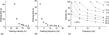
Since in the setup used, various process parameters of the flash lamp can be adjusted, the influence of each of those on the sintering behavior of printed silver lines was studied, keeping all other conditions constant. Fig. 3(a) shows how the sintering time of a silver nanoparticle ink depends on the lamp intensity at a flash frequency of 7 Hz. All intensities finally resulted in identical low resistance values, but only in the case of full intensity (100%; corresponding to 1000 W electrical power consumption) the sinter timescale reached 1–2 s. At lower intensities, a longer illumination time is required in order to achieve comparable resistances.
Parameter study of the process speed of photonic sintering. (a) Influence of intensity variation (flashing frequency 7 Hz). (b) Influence of frequency variation (flashing intensity 75%). (c) Summary indicating the combined influences of frequency and intensity on the sintering speed.

A similar situation was found when the flashing frequency was varied at constant lamp power (intensity) of 75% and pulse duration of 6 ms [Fig. 3(b)]. Clearly, a higher flashing frequency gives rise to faster sintering.
Not very surprisingly, the data indicate that increasing the total energy to which the sample line is exposed, either by increasing the energy per pulse or the frequency, results in a faster sintering process. The results have been summarized in Fig. 3(c), in which the sintering times are shown as a function of both the flashing frequency and light intensity. Obviously, to some extent an increase in frequency can compensate for the effect of a decrease in intensity and vice versa.
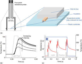
Although photonic sintering occurs much faster than conventional oven curing we assume it is nevertheless a purely thermal process. In this case, sintering would simply be highly accelerated by the strongly elevated temperatures reached for very short times in the ink lines and their immediate surroundings upon selective absorption of a light flash by the ink. Therefore, we have developed a temperature-sensing method which allows us to monitor the temperature development in an ink line during exposure to flash light. It consists of a fully sintered and thus highly conductive temperature probe line, which is covered by an isolating layer of dielectric material and a line of fresh (i.e., unsintered) ink on top [Fig. 4(a); cf. Supplementary Information for the exact dimensions of all the parts of the structure]. Whereas the fully sintered probe line is in electrical contact with a resistance meter, the unsintered line is not and serves purely to absorb the incoming radiation, heating the probe line via heat conduction through the dielectric material. After calibration in an oven (Fig. S5), the temperature dependence of the electrical resistance of the probe line can be used to follow the temperature changes in the wet ink during the flash illumination. Since the combined volumes of the probe line and isolation layer are two orders of magnitude smaller than that of the wet test line, they are expected to exert only minor influences on the temperature development in the test line. Furthermore, due to the small thickness of the isolation layer (500 nm), both metal lines are expected to reach thermal equilibrium faster than the shortest time interval between two measurements (1 ms), despite the rather low thermal conductivity of the dielectric material. Therefore, it can be assumed that the resistance of the probe line is a reliable measure for the temperature at the interface between wet ink and substrate, within the experimental error of the temperature measurement (±10 °C; cf. Supplementary Information).
Temperature monitoring during the sintering process. (a) Schematic illustration of the experimental setup. (b) Temperature development in an ink line after a single pulse of varying intensity (50–100%). (c) Combined temperature and resistance measurement for three bursts of three light flashes each.

As can be seen in Fig. 4(b), applying a single light pulse results in an almost immediate temperature increase in the ink line, with a peak value depending on the used intensity. Other factors expected to influence the temperature development are the thermal properties and absorption spectrum of the ink, as well as the cooling effect from solvent evaporation. At the end of the pulse, the temperature drops quickly due to heat transfer into the underlying substrate. Since the cooling rate is proportional to the temperature gradient, however, rather long times are necessary to cool fully down back to room temperature. Therefore, flashing at a constant frequency will either lead to a continuous heating of the foil until its glass temperature is reached and deformation occurs, or the process will be rather slow due to long cooling gaps and low flashing frequencies. As a compromise, however, we can also supply the energy in bursts of up to 32 pulses, followed by rather long cooling gaps. In this way, high temperatures can be built up and maintained for short times [Fig. S6 and Fig. 4(c)]. The number of pulses per burst can be adjusted to the thermal stability of the foil used. A rough estimate of the amount of energy put into the substrate via heat transfer from the ink line reveals that only a small fraction (below 1%; cf. Supplementary Information) of the total energy used will contribute to the heating of the plastic. Temperatures above the glass transition are thus not only limited in time, but also locally confined to the immediate surroundings of the ink line. This strategy allows fast sintering to be combined with only very limited damage to the substrate.
Although the setup presented in this publication only allows to sinter single lines, with some modifications to the apparatus the principle can also be applied for two-dimensional structures and on a roll-to-roll basis, as we have recently shown.[ Reference Galagan, Coenen, Abbel, van Lammeren, Sabik, Barink, Meinders, Andriessen and Blom 26 , Reference Abbel, van den Boomen, van Lammeren, de Koning, Valeton and Meinders 27 ]
Conclusions
In summary, we have demonstrated the combination of inkjet printing and photonic flash sintering as a versatile, fast and convenient processing technology for the production of highly conductive silver lines, as they are necessary in large area printed electronics. The key principles of our approach are localized heating of the ink by selective absorption, focusing the light to achieve high intensities, and the application of the energy in short pulses to limit heating of the underlying temperature-sensitive polymer substrate. A variety of process parameters, such as light intensity, flashing frequency or the number of pulses in one burst, can be varied in order to achieve optimized sintering conditions for different ink–foil combinations. Making use of this flexibility, we were able to achieve conductivities as high as 16% of the value of bulk silver within fractions of a second.
Supplementary materials
For supplementary material for this article, please visit http://dx.doi.org/10.1557/mrc.2012.28.