
Introduction
Since 2003, the renaissance of multiferroics has been stimulated by several seminal works, including the discoveries of magnetoelectric (ME) responses in single-phase multiferroic BiFeO3 (BFO) thin films,[ Reference Wang, Neaton, Zheng, Nagarajan, Ogale, Liu, Viehland, Vaithyanathan, Schlom, Waghmare, Spaldin, Rabe, Wuttig and Ramesh 1 ] magnetism-induced ferroelectricity in multiferroic manganites such as TbMnO3,[ Reference Kimura, Goto, Shintani, Ishizaka, Arima and Tokura 2 ] and strong ME coupling in CoFe2O4 (CFO)/BaTiO3 (BTO) multiferroic heterostructures,[ Reference Zheng, Wang, Lofland, Ma, Mohaddes-Ardabili, Zhao, Salamanca-Riba, Shinde, Ogale, Bai, Viehland, Jia, Schlom, Wuttig, Roytburd and Ramesh 3 ] unexpectedly igniting the tremendous flurry of interests in this field. The multiferroic nanostructures are of particular significance due to the high demand of the current miniaturization and multifunctional technological trends in microelectronic industry. In addition, the strong coupling between charge and spin degrees of freedom, i.e., the ME coupling in multiferroic nanostructures, allows for controlling magnetic order by electric field and vice versa.[ Reference Tokura 4 – Reference Wang, Liu and Ren 7 ] Over the last decade, this field has been expanding rapidly, and a number of novel phenomena and promising application opportunities have been reported.[ Reference Spaldin and Fiebig 8 – Reference Ratcliff, Lynn, Kiryukhin, Jain and Fitzsimmons 12 ]
Nowadays, device scale-down is being accelerated with the demands of high-performance and high-density data storage, while emergent physical phenomena can be expected when the materials are scaled down to nanoscale. Along this line, much attention has been attracted to developing new fabrication processes for high-density and high-quality multiferroic nanostructures, either single-phase materials or ferromagnetic/ferroelectric composites.[ Reference Han, Kim, Alexe, Hesse and Lee 13 , Reference Jung and Son 14 ] In ferroic nanodots, in contrast to the popular experimental works on ferromagnetic flux closure vortex domains,[ Reference Shinjo, Okuno, Hassdorf, Shigeto and Ono 15 – Reference Yamada, Kasai, Nakatani, Kobayashi, Kohno, Thiaville and Ono 17 ] the ferroelectric vortex domain structures remain experimentally elusive although theoretical predictions have been available for a long time.[ Reference Naumov, Bellaiche and Fu 18 ] Hence, a robust and controllable ferroelectric vortex remains highly favorable for future ultrahigh density applications. Besides, improved ME coupling in multiferroic nanodots,[ Reference Lu, Kim, Goetze, Li, Dong, Werner, Alexe and Hesse 19 , Reference Tian, Zhang, Yao, Fan, Li, Li, Song, Zhang, Qin, Zeng, Zhang, Yao, Gao and Liu 20 ] owing to the release of clamping effect from the substrates and proper manipulating of domain structures, paves a pathway to realize enhanced cross-controls of ferroelectricity and magnetism by magnetic and electric stimuli. In particular, this may provide opportunities for the room temperature reversible control of magnetism, which is of first priority for the next generation memory devices.[ Reference Tian, Zhang, Yao, Fan, Li, Li, Song, Zhang, Qin, Zeng, Zhang, Yao, Gao and Liu 20 , Reference Heron, Bosse, He, Gao, Trassin, Ye, Clarkson, Wang, Liu, Salahuddin, Ralph, Schlom, Iniguez, Huey and Ramesh 21 ] Finally, the cross-couplings among multiple functionalities such as strain, magnetism, polarization, and optical properties, have also drawn some research attentions, and further new findings and application potentials may be expected in this new exciting area.[ Reference Guo, You, Zhou, Shiuh Lim, Zou, Chen, Ramesh and Wang 22 – Reference Cherifi, Ivanovskaya, Phillips, Zobelli, Infante, Jacquet, Garcia, Fusil, Briddon, Guiblin, Mougin, Ünal, Kronast, Valencia, Dkhil, Barthélémy and Bibes 25 ]
In this mini-review, we emphasize on the domain structures and electric field control of magnetism in several multiferroic nanostructures. We will first introduce the schemes of connectivity between multiferroic nanostructures (e.g., nanodot arrays) and fabrication techniques. Then, a special focus on the flux closure polar vortex domains in ferroelectric nanodots will be described. Afterwards, the room temperature electric field control of nanoscale magnetic domain switching in various nanostructures, particularly the out-of-plane heterostructures compatible with the standard integrated electronics, will be reviewed. In the final section, future directions will be prospected. We genuinely hope that this mini-review will draw the readers' attention to the persistent challenges and future key directions in multiferroic nanostructures.
Different types of multiferroic nanostructures
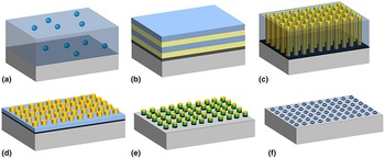
We first discuss several types of multiferroic composite nanostructures, which have been explored in the past decade, where the connectivity of the two and more components can greatly affect the ME properties. The most widely studied connectivity schemes include the 0–3 type particulate nanocomposite films, 2–2 type layered heterostructures, and 1–3 type vertical heterostructures,[ Reference Li, Levin, Slutsker, Provenzano, Schenck, Ramesh, Ouyang and Roytburd 26 – Reference Zhang, Miao, Tian, Lu, Zhao, Fan, Song, Li, Zeng, Gao and Liu 30 ] as shown in Figs. 1(a)–1(c). In the 0–3 type composites, magnetic particles are randomly distributed in ferroelectric matrix, while a 2–2 type layered heterostructure usually consists of alternating layers (two layers, multilayers, or even superlattices) of ferroelectric components and magnetic ones. The 1–3 type vertical heterostructures are typically made of pillars of one material embedded in the matrix of another. Quite a few excellent reviews addressing these 0–3, 2–2, and 1–3 types multiferroic nanostructures are available. In particular, the 1–3 type nanostructures are appreciated because they exhibit large ME coupling effect due to the efficient release of clamping effects from the substrates.[ Reference Nan, Bichurin, Dong, Viehland and Srinivasan 11 , Reference Ma, Hu, Li and Nan 31 – Reference Vaz, Hoffman, Ahn and Ramesh 33 ]
Schematics for different types of multiferroic nanostructures (a)–(f): (a) 0–3 type particulate nanocomposite films with magnetic particles embedded in the ferroelectric matrix, (b) 2–2 type layered heterostructures, (c) 1–3 type vertical heterostructures, (d) 0–2 type magnetic nanostructures on top of ferroelectric thin films, (e) 0–0 type layered heterostructured nanodot arrays, (f) multiferroic/ferroelectric/magnetic nanorings. The bottom layer (black color) in (b)–(e) is the bottom electrode, such as SrRuO3, La0.7Sr0.3MnO3, for studying the electric field control of magnetism in the multiferroic nanostructures.

Recently, several 0–0 and 0–2 types of nanostructures, as displayed in Figs. 1(d) and 1(e), have been reported.[ Reference Tian, Zhang, Yao, Fan, Li, Li, Song, Zhang, Qin, Zeng, Zhang, Yao, Gao and Liu 20 , Reference Heron, Bosse, He, Gao, Trassin, Ye, Clarkson, Wang, Liu, Salahuddin, Ralph, Schlom, Iniguez, Huey and Ramesh 21 , Reference Zhao, Lu, Zhang, Tian, Song, Li, Huang, Zhang, Qin, Wu, Lu, Zeng, Gao, Dai and Liu 34 , Reference Gao, Rodriguez, Liu, Birajdar, Pantel, Ziese, Alexe and Hesse 35 ] The 0–2 type multiferroic composites consist of ferroelectric films and magnetic nanostructures on top of them, allowing the electric field control of magnetic domain structures [Fig. 1(d)]. The less studied 0–0 type structures are mainly composed of ferroelectric–ferromagnetic epitaxial nanodot arrays [Fig. 1(e)] as well as recently reported multiferroic/ferroelectric/magnetic nanorings [Fig. 1(f)].[ Reference Tian, Zhang, Yao, Fan, Li, Li, Song, Zhang, Qin, Zeng, Zhang, Yao, Gao and Liu 20 , Reference Cho, Loget and Corn 36 ] Compared with those structures mentioned earlier, the 0–0 type nanodots arrays demonstrate several apparent advantages.[ Reference Lu, Kim, Goetze, Li, Dong, Werner, Alexe and Hesse 19 , Reference Tian, Zhang, Yao, Fan, Li, Li, Song, Zhang, Qin, Zeng, Zhang, Yao, Gao and Liu 20 ] First, they allow the atomic level mechanical coupling and concurrently avoid the substrate clamping in multiferroic composite films, benefiting to the ME coupling enhancement. The possibility for fabricating specific structures such as nanorings [Fig. 1(f)] and other multilayered geometries also enables us to explore additional geometric effects on domain structures and ME effects. Moreover, the 0–0 type multiferroic nanostructures are compatible with conventional semiconductor processing, with the ability to scale down to ultrahigh density and avoid the cross-talk effects among the neighboring dots. These advantages are highly preferred for applications in future multiferroic devices.
Fabrication of nanodot arrays
The fabrication of 0–3, 1–3, and 2–2 types of nanostructures have been addressed in previous review articles,[ Reference Nan, Bichurin, Dong, Viehland and Srinivasan 11 , Reference Wang, Hu, Lin and Nan 28 , Reference Vaz, Hoffman, Ahn and Ramesh 33 ] which is not our main focus. For high-density device applications and electric property characterizations of multiferroic nanostructures, the first priority is to fabricate high-quality epitaxial nano-island structures.[ Reference Scott 37 , Reference Ortega, Ashok, Scott and Ram 38 ] Along this line, several fabrication techniques developed in the past decade have been summarized by Han et al.,[ Reference Han, Kim, Alexe, Hesse and Lee 13 ] such as the top-down approaches including the focused ion beam milling and electron beam direct writing, the bottom-up self-assembly method, and the modified bottom-up membrane mask or copolymer template-assisted deposition. The self-assembled method to produce the 1–3 type nanostructures has been reviewed by Liu et al.[ Reference Liu, Liang, Chu, Zheng and Ramesh 32 ]
Furthermore, anodized alumina (AAO) template-assisted deposition method and the AAO template-assisted ion beam-etching technique have been attempted to produce high-quality epitaxial structures consisting of high-density 0–0 type ferroelectric/multiferroic nanodot arrays and nanorings.[ Reference Tian, Zhang, Yao, Fan, Li, Li, Song, Zhang, Qin, Zeng, Zhang, Yao, Gao and Liu 20 , Reference Tian, Zhao, Lu, Yao, Fan, Li, Li, Chen, Zhang, Qin, Zeng, Zhang, Dai, Gao and Liu 39 ] Here, we highlight several examples including those accomplished in the authors' laboratory. Tian et al.[ Reference Tian, Zhang, Yao, Fan, Li, Li, Song, Zhang, Qin, Zeng, Zhang, Yao, Gao and Liu 20 ] have just reported the fabrication of 0–0 type high-density and periodically ordered epitaxial CFO/BFO nanodot arrays by the AAO template-assisted pulsed laser deposition. As shown in Fig. 2(a), the AAO template mask was first transferred onto the SrRuO3 (SRO) buffered SrTiO3 (STO) substrate, and then the CFO/BFO nanodot arrays were sequentially prepared by pulsed laser deposition through the AAO template. Afterwards, the AAO mask was removed by mechanical or chemical lift-off to leave the nanodot arrays alone. The obtained nanodots exhibit an average lateral size of ~70 nm and neighboring dot–dot distance of ~110 nm [Fig. 2(b)]. The cross-section transmission electron microscopy (TEM) and selected-area electron diffraction confirmed the high quality and epitaxy of the BFO/CFO nanodot arrays [Figs. 2(c) and 2(d)]. In another work, Lu et al.[ Reference Lu, Kim, Goetze, Li, Dong, Werner, Alexe and Hesse 19 ] studied the similar 0–0 type BTO/CFO heterostructured nanostructures, which also exhibit some extent of ME coupling. This method enables a large-area fabrication of high-density well-ordered epitaxial nanodots, with the capability of scaling down to ~30 nm in diameter, yielding a pixel density higher than 100 Gbit/in.2.
Fabrication of high-density epitaxial nanodot arrays by AAO template-assisted pulsed laser deposition (a)–(d): (a) Schematics of fabrication procedures, (b) AFM image of the obtained nanodot arrays, (c) cross-section TEM images of a BFO/CFO/SRO nanodot, (d) selected area electron diffraction pattern of the nanodots. Reproduced from Ref. Reference Tian, Zhang, Yao, Fan, Li, Li, Song, Zhang, Qin, Zeng, Zhang, Yao, Gao and Liu20 by permission of © 2016 American Chemical Society. Preparation of epitaxial nanoring like structure, anti-nanodot arrays, and nanodot arrays by AAO template-assisted ion beam etching method are demonstrated in (e)–(h):[ Reference Tian, Zhao, Lu, Yao, Fan, Li, Li, Chen, Zhang, Qin, Zeng, Zhang, Dai, Gao and Liu 39 ] (e) Schematic diagram for the AAO template-assisted ion beam-etching method. Panels (f)–(h) show the AFM images for the corresponding BFO nanostructure arrays produced after different etching durations from 5 to 25 min: (f) nanorings, (g) anti-nanodot arrays, and (h) nanodot arrays.

In addition, a novel route to fabricate the BFO nanodots and nanorings was proposed,[ Reference Tian, Zhao, Lu, Yao, Fan, Li, Li, Chen, Zhang, Qin, Zeng, Zhang, Dai, Gao and Liu 39 ] as illustrated in Fig. 2(e). Here, ion beam was used to etch the high-quality single-phase multiferroic BFO film through the AAO-template mask. By this approach, the BFO nanorings, nanodot arrays, and anti-nanodot arrays, can be fabricated by simply adjusting the etching duration, as shown in Figs. 2(f)–2(h). The step-by-step SEM study revealed the morphology evolution of the AAO mask layer from hole-array to dot-array during the etching process, and consequently the BFO film underneath the AAO template evolved into various nanostructured arrays. This method can also be extended to pattern a wide range of multiferroic/ferroelectric/magnetic nanostructures with adjustable shape, size, and pixel density, and it is thus promising in terms of fundamental research and for applications in high-density devices such as ultra-high-density recording devices.
Topological flux closure vortex domain structures
Domain structures are rather essential for ferroic materials, which not only greatly affect the ferroic functionalities such as piezoelectricity, electrical conductivity, magnetic exchange bias, but also largely determine the coupling between the inter-ferroic orders in multiferroic materials. It is suggested that the domain structures are critically dependent of the interplay among various energies such as exchange, electroelastic, and electrostatic energies with adjacent surface. All these ingredients of physics are however highly dimensionality-relevant.[ Reference Catalan, Seidel, Ramesh and Scott 40 ] Consequently, dimension reduction in ferroic nanostructures becomes an effective tool to manipulate the domain structures. Ferroic nanodot represents a typical geometry to illustrate such manipulation. In this section, we will pay attention to the nanoscale domain structures in ferroic nanodots, including several types of multiferroic nanodots.
Earlier investigations did explore several unique domain structures in ferroic nanostructures, such as single domain dots, bubble domains, and one-dimensional (1D) topological defects such as vortex, center types, and skyrmion domain structure, depending on different kinds of materials and geometries.[ Reference Shinjo, Okuno, Hassdorf, Shigeto and Ono 15 , Reference Catalan, Seidel, Ramesh and Scott 40 , Reference Gao, Xue, Qin, Liu, Rodriguez, Liu, Alexe and Hesse 41 ] One of the most interesting systems is the flux closure vortex topological structures, which exist in nature over a wide range of scales, from galaxies and weather systems down to the flowers, as illustrated in Fig. 3(a). These exotic vortex topological defects in multiferroic/ferroelectric/magnetic materials are also attracting intensive attentions. Landau and Lifschitz[ Reference Landau and Lifschitz 42 ] and Kittel[ Reference Kittel 43 ] first predicted that the flux closure vortex domain structures possibly occur in ferromagnetic nanodots. Indeed, the vortex (skyrmion) structures in nanosized ferromagnets have been frequently reported due to their prominent demagnetization effect.[ Reference Shinjo, Okuno, Hassdorf, Shigeto and Ono 15 , Reference Guslienko, Han, Keavney, Divan and Bader 44 ] It was intensively studied for the purpose of high-density data storage. The skyrmion in ferromagnetic/multiferroic materials as a hot topic nowadays has also been observed in systems with large Dzyaloshinsky–Moriya (DM) effect.[ Reference Seki, Yu, Ishiwata and Tokura 45 ]
(a) Flux closure vortex structures in nature: galaxies system, weather system, and a flower. (b) A vortex in a ferroelectric nanodot along the central z-plane, and (c) arrays of vortices appear in the central x (as well as y) cross-section, theoretically predicted by Naumov et al. Reproduced from Ref. Reference Naumov, Bellaiche and Fu18 by permission of © 2004 Nature Publishing Group. (d) Ferroelectric domains within the quadrants in BaTiO3 nanodots, observed by TEM. Reproduced from Ref. Reference Schilling, Byrne, Catalan, Webber, Genenko, Wu, Scott and Gregg46 by permission of © 2009 American Chemical Society. (e) Vortex polarization states in PZT nanodots. Reproduced from Ref. Reference Gruverman, Wu, Fan, Vrejoiu, Alexe, Harrison and Scott47 by permission of © 2009 American Chemical Society. (f) Flux closure vortex–antivortex arrays in PTO/STO superlattices, obtained by HRTEM. Reproduced from Ref. Reference Yadav, Nelson, Hsu, Hong, Clarkson, Schlepuetz, Damodaran, Shafer, Arenholz, Dedon, Chen, Vishwanath, Minor, Chen, Scott, Martin and Ramesh48 by permission of © 2016 Nature Publishing Group.

On the other hand, experimental observations of flux closure vortex domain in ferroelectrics are still elusive, although a number of theories predicted the existence of ferroelectric vortex.[ Reference Naumov, Bellaiche and Fu 18 , Reference Naumov and Fu 49 , Reference Wu, Huang, Liu, Wu, Duan and Gu 50 ] Unlike the well-known skyrmion in nanosized ferromagnets, the flux closure vortex domains in ferroelectrics suffer from large electroelastic energy. Nevertheless, size reduction can help releasing such large electroelastic energy. In 2004, Naumov et al.[ Reference Naumov, Bellaiche and Fu 18 ] predicted that bi-stable polar vortex as small as 3.2 nm can be stable in highly depolarized ferroelectric nanodots [Figs. 3(b) and 3(c)], promising for ultrahigh storage density of 60 Tbit/in.2, two orders of magnitude higher than conventional nonvolatile memories. In the meantime, since the interaction between vortex domains in different dots is generally weak, the problem of cross-talking between different memory units can thus be largely avoided. These advantages aroused a surge of research interests, and tremendous efforts have been placed on seeking ferroelectric vortex domains in various nanodots. Experimental evidences with the flux-closure domain structures have not been unveiled until recently, thanks to the emergence of powerful piezoresponse force microscopy (PFM) and advanced TEM technique.[ Reference Catalan, Seidel, Ramesh and Scott 40 , Reference Schilling, Byrne, Catalan, Webber, Genenko, Wu, Scott and Gregg 46 , Reference Gruverman, Wu, Fan, Vrejoiu, Alexe, Harrison and Scott 47 , Reference Rodriguez, Gao, Liu, Lee, Naumov, Bratkovsky, Hesse and Alexe 51 , Reference Li, Li, Yu, Chen and Xie 52 ] Nelson et al.[ Reference Nelson, Winchester, Zhang, Kim, Melville, Adamo, Folkman, Baek, Eom, Schlom, Chen and Pan 53 ] and Jia et al.[ Reference Jia, Urban, Alexe, Hesse and Vrejoiu 54 ] identified half of a closure quadrant at the junction between ferroelectric domain walls and an interface in thin films of BFO and PbTiO3 (PTO), respectively. The full closure quadrant was found by Gruverman et al.,[ Reference Gruverman, Wu, Fan, Vrejoiu, Alexe, Harrison and Scott 47 ] McGilly et al.,[ Reference McGilly, Schilling and Gregg 55 ] and McQuaid et al.[ Reference McQuaid, McGilly, Sharma, Gruverman and Gregg 56 ] in ferroelectric BaTiO3 nanodots [Fig. 3(d)]. Rodriguez et al.[ Reference Rodriguez, Gao, Liu, Lee, Naumov, Bratkovsky, Hesse and Alexe 51 ] revealed the vortex polarization states in Pb(Zr,Ti)O3 (PZT) nanodots using PFM assisted with theoretical predictions [Fig. 3(e)]. However, flux closure polarization vortex was not yet demonstratively observed in spite of available indirect evidence with their transient forms during the switching process,[ Reference Gruverman, Wu, Fan, Vrejoiu, Alexe, Harrison and Scott 47 ] until direct observations of the flux-closure domains and polar vortex in PTO/STO multilayers[ Reference Tang, Zhu, Ma, Borisevich, Morozovska, Eliseev, Wang, Wang, Xu, Zhang and Pennycook 57 ] and their superlattices [Fig. 3(f)],[ Reference Yadav, Nelson, Hsu, Hong, Clarkson, Schlepuetz, Damodaran, Shafer, Arenholz, Dedon, Chen, Vishwanath, Minor, Chen, Scott, Martin and Ramesh 48 ] respectively. The vortex domains are promising towards future nanoelectronics applications since their low dimensionality and specific momenta. These works pave the way to utilize the geometric parameters of ferroic nanostructures to tailor their domain structures and other related novel properties such as ME coupling, and the relevant techniques appear to be competitive for domain engineering and domain electronics.
Electric field control of magnetism
Electric field control of magnetism in multiferroics, aiming at new types of ultra-low-power consuming and high-density memories/logic devices, has been the focus of intensive researches.[ Reference Wang, Liu and Ren 7 , Reference Chu, Martin, Holcomb and Ramesh 58 , Reference Vaz 59 ] In the multiferroic composites, electric field control of magnetism can be realized by means of either strain-mediated ME coupling across the interface, exchange coupling, or charge-driven ME coupling.[ Reference Nan, Bichurin, Dong, Viehland and Srinivasan 11 , Reference Wang, Hu, Lin and Nan 28 , Reference Ma, Hu, Li and Nan 31 , Reference Vaz, Hoffman, Ahn and Ramesh 33 ] In another word, the ME effects can be obtained by the coupling between interfacing ferroelectric and ferromagnetic domains, leading to magnetic domain switching indirectly driven by ferroelectric domain switching triggered by electric field. Currently, the key challenge for the electrical control of magnetism is to achieve robust and reversible 180° switching of magnetization by electric field at room temperature. Nanoscale multiferroic nanostructures favor the domain structure manipulation, substrate clamping release, and domain stability alternation, while all of these mechanisms are effective roadmaps to achieve this goal.
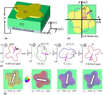
We highlight several instances along this line. For a 0–2 type multiferroic system consisting of nickel nanomagnet on piezoelectric Pb(Mg1/3Nb2/3)O3–PbTiO3 (PMN–PT) single-crystal substrate, the elastic coupling stems from the piezoelectric/magnetostrictive coupling via the interface, in which the ME coupling is indirect. It is rather difficult to realize the 180° switching of magnetic domains in such structure due to the twofold degeneracy of magnetization. However, if one takes advantage of the shape anisotropy by designing a specific geometric structure, the 180° domain switching can be obtained by applying two consequent electric pulses, as shown in Fig. 4. In the first negative electric pulse, the piezoelectric substrate PMN–PT generates a compressive strain on the nanomagnet, which provides an extra anisotropy with the easy axis along the x-axis to rotate the magnetic orientation for 90°. The second positive electric pulse generates an easy axis along the y-axis, leading to another 90° rotation; thus a 180° reverse can be achieved.[ Reference Wang, Hu, Ma, Zhang, Chen and Nan 60 ] This indicates that it is possible to achieve the 180° domain switching of nanomagnets by properly adjusting the shape anisotropy and interface coupling.
Morphologically engineered artificial multiferroic heterostructure. (a) Schematic of the heterostructure of a patterned nanomagnet with fourfold shape symmetry grown on a ferroelectric layer [e.g., (011)-PMN–PT]. (b) The top view of the Ni nanomagnet on the ferroelectric layer, where y-axis denotes the main direction of in-plane anisotropic piezostrain and the angle between y-axis and one of the long axes of the Ni nanomagnet. The blue dashed line represents the shape anisotropy energy contour at initial states. Mechanisms of the 180° reversal: (c) Energy polar diagrams of the Ni nanomagnet upon the application of zero electric field (as-grown state), and then successive fields of −E
c, E
c, and zero. Here the gray-dashed and magenta-solid arrows represent the previous and present states of m, respectively, and the energy barrier ΔE = E
2 − E
1 ensures the magnetization switch unidirectionally from  state to
 state, and from
 state to
 state, respectively. (d) Magnetization vector diagrams corresponding to (c), in which the different background colors represent the orientations of the magnetization as indicated by the color wheel. Reproduced from Ref. Reference Wang, Hu, Ma, Zhang, Chen and Nan60 by permission of © 2014 Nature Publishing Group.

Electric field control of nanoscale magnetic domain through the exchange coupling between antiferromagnetic BFO and magnetic nanostructures was also explored. In 2006, Zhao et al.[ Reference Zhao, Scholl, Zavaliche, Lee, Barry, Doran, Cruz, Chu, Ederer, Spaldin, Das, Kim, Baek, Eom and Ramesh 61 ] demonstrated the room temperature electric field control of antiferromagnetic order in multiferroic BFO films. Later, Chu et al.[ Reference Chu, Martin, Holcomb, Gajek, Shu Jen, Qing, Balke, Chan Ho, Lee, Wei, Qian, Pei Ung, Rodriguez, Scholl, Wang and Ramesh 62 ] successfully reversibly rotated the in-plane magnetic domain of Co0.9Fe0.1 (CoFe) nanomagnets for 90° at room temperature by electric field, using the exchange coupling-mediated ME effect in the CoFe/BFO system, a 0–2 type structure. In the latter study, a room temperature in-plane electric field induced 180° magnetization reversal was achieved, through the in-plane switching of stripe-like 71° ferroelectric domain pattern.[ Reference Heron, Trassin, Ashraf, Gajek, He, Yang, Nikonov, Chu, Salahuddin and Ramesh 63 ] From a device point of view, it is more important to achieve an out-of-plane electric field control of magnetism, which is more compatible with current microelectronic device process. Recently, Heron et al.[ Reference Heron, Bosse, He, Gao, Trassin, Ye, Clarkson, Wang, Liu, Salahuddin, Ralph, Schlom, Iniguez, Huey and Ramesh 21 ] reported a seminal work on the out-of-plane electric field deterministic control of magnetism at room temperature in the CoFe/BFO spin valve device, using the exchange-mediated ME effects [Fig. 5(a)]. To probe the domain structures and the net magnetic moment, the x-ray magnetic circular dichroism photoemission electron microscopy (XMCD-PEEM) images of the Pt/CoFe/BFO system were taken in the initial state and after application of 6 V, where the incident x-ray was aligned perpendicular and parallel to the stripe like 71° domains [Fig. 5(b)], respectively. It turns out that the net CoFe magnetization can be reversed by applying an electric field as low as 6 V [Fig. 5(c)], thanks to the coupling between the magnetic DM vector and ferroelectric polarization in the BFO layer. However, the reliability issue for such reversible switching is still a great challenge for the actual device applications, as it is still difficult to obtain more than three switching cycles in the current devices.
Electric field control of magnetism in a 0–2 type multiferroic nanostructure (a)–(c): (a) Schematic of a ME device consisting of either CoFe or a Co0.9Fe0.1/Cu/CoFe spin valve on BiFeO3. (b) Initial and final (after 6 V) directions of the in-plane CoFe moments imaged with a vertical K X-ray and horizontal K X-ray XMCD-PEEM. (c) The domain pattern switches and net CoFe magnetization reverses after the voltage is applied. Scale bars are 2 µm in (b) and (c). Reproduced from Ref. Reference Heron, Bosse, He, Gao, Trassin, Ye, Clarkson, Wang, Liu, Salahuddin, Ralph, Schlom, Iniguez, Huey and Ramesh21 by permission of © 2014 Nature Publishing Group. Electric field control of magnetization in 0–0 type multiferroic nanostructured nanodot arrays (d)–(f): (d) AFM topology image, (e) MFM micrograph superimposed with its corresponding 3D topographic image. (f) The selected area magnified MFM images superimposed with their 3D topologies before and after applying electric field of ±8.5 V bias voltages. Reproduced from Ref. Reference Tian, Zhang, Yao, Fan, Li, Li, Song, Zhang, Qin, Zeng, Zhang, Yao, Gao and Liu20 by permission of © 2016 American Chemical Society.

In addition, the out-of-plane electric field control of magnetic domain switching in 0–0 type multiferroic structures is also highly desired. Recently, the 0–0 type CFO/BFO heterostructured nanodots have been developed by Tian et al.,[ Reference Tian, Zhang, Yao, Fan, Li, Li, Song, Zhang, Qin, Zeng, Zhang, Yao, Gao and Liu 20 ] and the electric field control of magnetization reversal based on a combination of strain-mediated and exchange-mediated ME effects was also demonstrated, as shown in Figs. 5(d)–5(f). To display the domain structure evolution in the nanodot arrays, the magnetic force microscopy (MFM) images were superimposed onto the corresponding 3D surface topology images, as shown in Fig. 5(e). An apparent variation of the MFM contrast occurred upon the electric field poling. For a clearer presentation, two small regions were pitched up to illustrate the domain switching in a bigger magnification. One sees clearly the magnetization switching of the nanodots to the opposite orientations, as reflected by the apparent contrast reversal shown in the MFM image [Fig. 5(f)]. Although such electric-field-induced magnetic switching is not well controllable, an opportunity for low-energy-consumption and high-density recording devices is open.
Outlook
Currently, exciting findings in nanostructured multiferroics have been obtained, which triggers interest in new mechanisms and methods to tailor the inter-ferroic couplings. In particular, novel aspects of electric field control of magnetic domain switching are highly appealed. However, there are still some further studies needed to achieve breakthroughs and to push this area to real applications.
Fabrication of high-density arrays
With the continued demand for ultra-high-density data storage applications, it is becoming increasingly important to scale down the dimension of multiferroic structures to nanoscale arrays such as nanodot arrays. However, there is a great challenge to prepare high-quality nanodots with diameter below 30 nm using the traditional AAO template process, since this method requires very stringent deposition parameters that are unfavorable, and smaller pore mouth would be more easily blocked during the deposition of multiferroic materials. Polystyrene spheres template with ion beam-etching method could be another alternative. Our unpublished research shows that this method can be a facile route to fabricate high-quality multiferroic nanodot arrays with excellent epitaxial structure and multiferroic properties close to their parent films. Small copolymer templates could also be used to obtain nanodots as small as ~20 nm; however, their overall quality and order arrangement need to be further improved.
Domain design and manipulation
Although some indications of flux closure vortex-like behaviors are available, there is still no direct evidence with the ferroelectric flux closure vortex in isolated multiferroic/ferroelectric nanodots, while well-established vortex in PTO/STO superlattices was reported.[ Reference Yadav, Nelson, Hsu, Hong, Clarkson, Schlepuetz, Damodaran, Shafer, Arenholz, Dedon, Chen, Vishwanath, Minor, Chen, Scott, Martin and Ramesh 48 ] The difficulty lies in that a simple quadrant arrangement generates enormous disclination strain, which prevents the formation of vortex. If the size of nanodot is smaller than the critical point, alleviation of associated stresses will allow the depolarization effect to turn the polarization into flux closure vortex domain. Thus, sufficiently small size and high depolarization field are required to achieve the vortex domain, as supported by the observation of vortex arrays in PTO/STO superlattices, which is well consistent with the prediction by Naumov et al.[ Reference Naumov, Bellaiche and Fu 18 ] In addition, multiferroic/ferroelectric nanorings may help to stable the vortex configuration due to the absence of highly energetic vortex core. Moreover, whether the vortex structure can be manipulated by external stimuli, e.g., a robust and electric field well-controllable vortex domain, is still the target of further efforts. Furthermore, other ferroelectric topologic domain structures such as skyrmions and center domain also need further explorations, which may lead to new discoveries as well as application potentials.
Besides, geometric effect in nanodots is an effective tool to manipulate both ferroelectric and magnetic domain structures as well, which provides a new method to tailor the ME effects. Previous work demonstrated that it is possible to achieve electric field induced 180° magnetic switching.[ Reference Heron, Bosse, He, Gao, Trassin, Ye, Clarkson, Wang, Liu, Salahuddin, Ralph, Schlom, Iniguez, Huey and Ramesh 21 ] Further work is still needed to obtain reversible switching in high-density nanodot arrays to pave the way for devices applications.
Room temperature electric field control of exchange bias
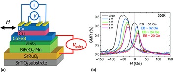
In the ferromagnet/BFO heterostructures, the exchange bias arising from the BFO domain walls and ME coupling between the ferromagnetic layer and antiferromagnetic BFO layer offer another possibility to achieve room temperature electric field control of exchange bias. Reversible electric field control of exchange bias has been achieved in a LaSr0.7Mn0.3O3/BiFeO3 (LSMO/BFO) field effect device structures, however, it has to be done below 10 K.[ Reference Wu, Cybart, Yu, Rossell, Zhang, Ramesh and Dynes 64 , Reference Wu, Cybart, Yi, Parker, Ramesh and Dynes 65 ] Martin et al.[ Reference Martin, Chu, Zhan, Ramesh, Han, Wang, Warusawithana and Schlom 66 , Reference Martin, Chu, Holcomb, Huijben, Yu, Han, Lee, Wang and Ramesh 67 ] have demonstrated a very large room temperature exchange bias (150–200 Oe) in the CoFe/BFO system, but electric field control of exchange bias has not yet been demonstrated. Recently, Allibe et al.[ Reference Allibe, Fusil, Bouzehouane, Daumont, Sando, Jacquet, Deranlot, Bibes and Barthélémy 68 ] reported that the exchange bias can be electrically manipulated in a CoFeB/BFO-based spin valve, revealed by giant magnetoresistance (GMR) measurement (Fig. 6). Nevertheless, the switching is not very reversible, and they failed to restore any exchange bias in the subsequent cycles by applying the opposite voltage or by other voltage protocols. One possible reason is that the exchange bias arises from the pinned uncompensated spins at 109° domain walls of BFO, while the 109° domains are gradually switched to 71° domains or mono-domains (which has no pinned uncompensated spins) upon further polarization reverse cycles, resulting in the decline of exchange bias.[ Reference Martin, Chu, Holcomb, Huijben, Yu, Han, Lee, Wang and Ramesh 67 , Reference Bea, Bibes, Ott, Dupe, Zhu, Petit, Fusil, Deranlot, Bouzehouane and Barthelemy 69 ] Therefore, stable and reversible electric field switching of 109° domains is crucial for achieving room temperature reversible electric field control of exchange bias. Specific techniques, such as using multiferroic BFO nanodots, which will reduce the clamping effect from the substrate, may help to solve this problem.
(a) Schematic of the spin valve device. (b) GMR curves of the spin valve after different electric pulses applied. Reproduced from Ref. Reference Allibe, Fusil, Bouzehouane, Daumont, Sando, Jacquet, Deranlot, Bibes and Barthélémy68 by permission of © 2012 American Chemical Society.

Cross-couplings between strain, ferroelectricity, magnetism, and optical properties
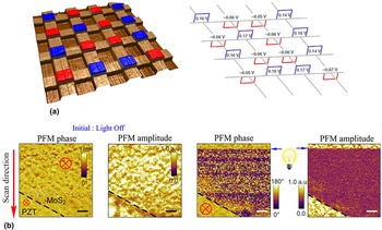
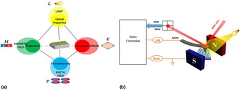
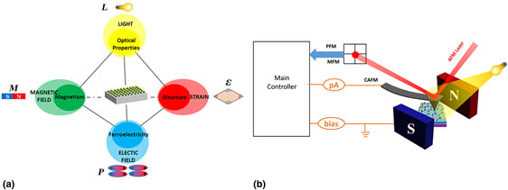
In literature on multiferroics, ME coupling is the main focus, while some more couplings may occur among strain, ferroelectricity, magnetism, and optical properties, which may give rise to multifunctional cross-couplings. For instance, a ferroelectric photovoltaic prototype 16-cell memory shown in Fig. 7(a) reveals the coupling between ferroelectricity and photovoltaic properties, allowing the polarization modulation of photovoltaic properties.[ Reference Guo, You, Zhou, Shiuh Lim, Zou, Chen, Ramesh and Wang 22 ] And optical light-induced ferroelectric switching was also reported in PZT films with molybdenum disulfide (MoS2) transparent top electrodes by Gruverman's group [see Fig. 7(b)].[ Reference Lipatov, Sharma, Gruverman and Sinitskii 24 ] Chu and co-workers demonstrated the phenomenon of magnetic switching triggered by an ultrafast layer beam in CFO/SRO (1–3) type columnar composite, through the photorestriction from SRO layer.[ Reference Liu, Chen, He, Liang, Chen, Chien, Hsieh, Lin, Arenholz, Luo, Chueh, Chen and Chu 23 ] The ferroelectric control of field-effect transistors enhanced using monolayer black phosphorus as the interfacial layer was predicted.[ Reference Liu, Zhou, Wang, Liu, Wang and Guo 70 ] The coexistence of remarkable structural, ferroelectric, magnetic, and optical properties, as well the cross-couplings among them [see Fig. 8(a)], with the inputs of strain, electric field, magnetic field, and light, endows multiferroic nanostructures with a unique potential for multifunctional devices in electronics, spintronics, piezotronics, photonics, etc. providing a fantastic playground to engineer novel physical properties. To explore the nanoscale cross-couplings in low-dimensional nanostructures, new nanoscale multi-physic properties testing and tailoring systems are very indispensable, such as a multifunctional scanning probe microscopy (SPM) system [Fig. 8(b)], which enables in-situ measurements of PFM, MFM, conductive atomic force microscopy (C-AFM), and near-field optical properties, under various electric field, magnetic field, optical light, heat, and environmental conditions.
(a) A prototype of a 16-cell ferroelectric photovoltaic memory based on the cross-bar architecture, in which the photovoltaic voltages can be switched by the polarization reversal. Reproduced from Ref. Reference Guo, You, Zhou, Shiuh Lim, Zou, Chen, Ramesh and Wang22 by permission of © 2013 Nature Publishing Group. (b) Optical light induced polarization switching in PZT with MoS2 top electrodes, in which one can see the apparent contrast change in both PFM phase and amplitude after illumination of optical light. Reproduced from Ref. Reference Lipatov, Sharma, Gruverman and Sinitskii24 by permission of © 2015 American Chemical Society.

(a) Sketch of possible couplings between the various functionalities. (b) A proposed multifunctional SPM system for characterization of multifunctional couplings, which enables in situ measurements of PFM, MFM, C-AFM, and near-field optical properties, under various electric field, magnetic field, optical light, heat, and environmental conditions.

Acknowledgments
The authors would like to thank the Natural Science Foundation of China (Grant No. 51272078, 51431006), the Project for Guangdong Province Universities and Colleges Pearl River Scholar Funded Scheme (2014), Science and Technology Planning Project of Guangdong Province (Grant No. 2015B090927006), the Natural Science Foundation of Guangdong Province (Grant No. 2016A030308019), and the International Science & Technology Cooperation Platform Program of Guangzhou (Grant No. 2014J4500016).