Introduction
As we reach the end of the silicon technology roadmap, alternative materials such as high mobility GeReference Kuzum, Krishnamohan, Nainani, Sun, Pianetta, Wong and Saraswat1, Reference Nakakita, Nakane, Sasada, Matsubara, Takenaka and Takagi2 and III–VcompoundsReference Radosavljevic, Chu-Kung, Corcoran, Dewey, Hudait, Fastenau, Kavalieros, Liu, Lubyshev, Metz, Millard, Mukherjee, Rachmady, Shah and Chau3–Reference Kim and del Alamo5 have proven to be strong contenders for extending high performance logic beyond the 22 nm technology node. However, before these technologies can be implemented, a few of the existing problems must be solved. These include the gate dielectric to channel interface, integration on silicon, a smaller device footprint in line with the device density improvement expected of each successive technology node, and low-resistance source/drain contacts, where the latter is related to the formation of Schottky barriers.
In the case of Ge metal oxide semiconductor field-effect transistors (MOSFETs), high-performing pMOSFETs have already been demonstrated, but Ge nMOSFETs still have much room for improvement. Ge nMOSFET performance is currently limited by high interface trap density at the gate dielectric, which causes inversion charge loss through trapping,Reference Kuzum, Krishnamohan, Nainani, Sun, Pianetta, Wong and Saraswat1 and large source/drain (S/D) parasitic resistance (R SD), which results in the measured extrinsic performance falling far behind the intrinsic performance. The high R SD is a combined result of low n-type dopant solubility and Fermi-level pinning in the source/drain regions. Strong Fermi-level pinning at the metal/semiconductor interface is observed when metal work functions are varied from 2.8 eV (Ce) to 5.6 eV (Pt), but the Schottky barrier height was found to only vary from 0.49 to 0.64 eV.Reference Dimoulas, Tsipas, Sotiropoulos and Evangelou6 The roughly 0.5 eV barrier height is also far from the near zero barrier needed for good ohmic contacts. Recent work on sulfur-passivated Ni germanide contacts to n-Ge has demonstrated barriers as low as 0.15 eV,Reference Ikeda, Yamashita, Sugiyama, Taoka and Takagi7 which is promising, but the current-voltage characteristics remain rectifying.
For III–V compound semiconductors, Fermi-level pinning also results in high Schottky barrier heights, and in materials with large bandgaps such as GaAs (1.42 eV), the pinned barrier can be fairly large, ranging from 0.7 to 1.0 eV.Reference Myburg, Auret, Meyer, Louw and van Staden8 Without the silicidation technology available to Si and the germanide technology for Ge, III–V materials rely on multilayered alloyed structures to form ohmic contacts (for example Au/Ge/Ni in the case of GaAs). These S/D contact materials can then diffuse up to hundreds of nanometers during alloying, so in order to prevent electrical shorting, most promising III–V FET/high-electron-mobility transistors (HEMTs) demonstrated have S/D spacings in the micron scale, despite nanometer scale gate lengths.
In recent work on non-alloyed contacts to HEMTs, Waldron et al.Reference Waldron, Kim and del Alamo9 had a 60 nm contact-to-gate separation using W to contact In0.65Ga0.35As with a doping density of 2 × 1019 cm–3. Singisetti et al.Reference Singisetti, Wistey, Zimmerman, Thibeault, Rodwell, Gossard and Bank10 achieved a low resistance of 1.3 Ω μm2 using in situ Mo on n-In0.53Ga0.47As with doping of 8 × 1019 cm–3. However, in both studies, the contacts were made to very highly doped molecular beam epitaxy-grown substrates with considerable tunneling current to facilitate the contact. A challenge remains in making a non-alloyed ohmic contact to lower doped materials, which is a long-standing problem for III–V MOSFETs due to poor S/D dopant activation in ion implanted self-aligned S/D. Higher temperature annealing is needed for greater dopant activation, but temperatures above 700°C also cause arsenic to desorb from the surface and induce negative charges and interface traps, which degrade the InGaAs surface and therefore the mobility of III–V surface channel MOSFETs.Reference Yasuda, Ishii, Urabe, Itatani, Miyata, Yamada, Fukuhara, Hata, Yokoyama, Takenaka and Takagi11
As complementary metal oxide semiconductor (CMOS) scaling continues, S/D junction depths are increasingly shallower in order to control short channel effects. However, the shallow junction adversely results in a rapid increase in parasitic resistance, which could then degrade the overall device performance.Reference Wong, Wei and Deng12 Metal S/D Schottky barrier transistors (SB-FETs) offer a solution, but they require low barriers (<0.1 eV) at the S/D for sufficient on-current.Reference Connelly, Faulkner, Grupp and Harris13 Until recent work by Connelly et al.,Reference Connelly, Faulkner, Grupp and Harris13 which showed a reduction of the metal/Si Fermi-level pinning through the use of an ultrathin Si3N4, the formation of large Schottky barriers had limited the implementation of Ge SB-FETs and III–V SB-FETs.
In this article, we discuss the use of thin dielectrics to alleviate metal/semiconductor Fermi-level pinning of high mobility materials. We then examine the contact design parameters involved to minimize the resulting effective barrier height and contact resistance for S/D contacts. The low achievable active n-type doping along with the high diffusion coefficients of dopants in Ge make it difficult to fabricate shallow, highly activated p-n junctions with low off-state current. However, with low enough barrier heights, Ge SB-FETs are shown to offer a viable solution to circumvent the problem. Furthermore, the ability to reduce the III–V Schottky barrier also allows for the use of a non-alloyed S/D contact, which is critical in the scalability of III–V MOSFETs for the application of future generations.
Metal/semiconductor Fermi-level pinning
Pinning theories
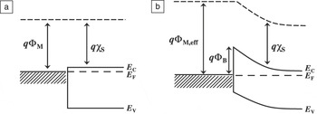
According to the Schottky-Mott theory,Reference Schottky14 when a metal and semiconductor are brought into contact, the two Fermi levels align, so the semiconductor Fermi level at the interface is modified. The potential barrier ΦB between the two should ideally be set by the metal work function ΦM and semiconductor electron affinity χS, where ΦB = ΦM – χS for an n-type semiconductor. However, in reality, this dependence is not experimentally observed. Schottky barrier heights tend to be pinned at a value roughly independent of the metal work function, as shown in Figure 1.
(a) Band diagram of an ideal unpinned Schottky barrier, where q represents the electronic charge, ΦM is the metal work function in vacuum, and χS is the semiconductor electron affinity. (b) Band diagram of a pinned Schottky barrier where the effective metal work function ΦM,eff is modeled as differing from the work function in vacuum ΦM. The Schottky barrier height is indicated by ΦB. E C is the conducting band energy, E V the valence band energy, and E F the Fermi energy level.

Currently, there are two popular Fermi-level pinning theories, where the origin of the pinning states varies with the model. Two of the more popular ones are the metal-induced gap states (MIGS) and bond polarization theories.
Heine first proposed the MIGS theory in 1965,Reference Heine15 which was later supported by Tersoff.Reference Tersoff16 The basis of this theory is that wave functions of electrons in the metal tail can decay into the semiconductor in the forbidden bandgap energy range, creating intrinsic states known as the metal-induced gap states. Near the valence band, these states are found to be mostly donor-like, and near the conduction band, they are mostly acceptor-like. The charge neutrality level (E CNL) is then the energy level at which the interface states change from mostly donor-like to acceptor-like. In a metal/semiconductor junction, the charging of these states by the metal wave function creates a dipole charge that causes the Fermi level, E F, to align to minimize the dipole charge toward zero, effectively pulling the E F at the interface toward E CNL. How close the interface E F is to E CNL is determined by the semiconductor’s dielectric screening or pinning factor S,Reference Yeo, King and Hu17 through the relationship

S is empirically found to be inversely related to the electronic component of the dielectric constantReference Mönch18 ε∞, and ranges from 0 to 1. The effective metal work function is given by ΦM,eff, while the work function at the charge neutrality level is given by ΦCNL. Semiconductors tend to have a smaller S than oxides and other dielectrics, which explains why generally Fermi-level pinning does not exist in metal/oxides junctions.
Tung’s bond polarization theoryReference Tung19 is similar to the MIGS theory in the idea of gap states being the source of Fermi-level pinning. However, the difference in Tung’s theory is the idea that the gap states arise from the bond polarization of the chemical bonds at the metal semiconductor interface, while in MIGS, it is assumed that the distribution of gap states is only a function of the semiconductor, with no dependence on the metal. In actuality, there must be a rearrangement of charge in forming the chemical bonds between the metal and semiconductor in order to satisfy thermodynamics and the minimization of interface energy. This interaction of metal and semiconductor wave functions at a Schottky junction are accounted for in the formation of an interface specific region, where the electronic states are not fully metal or semiconductor-like, but rather a mixture of the two. Minimization of the total interface energy causes the metal and semiconductor charge density to relax, creating an interface dipole that pins the Fermi level.
Fermi-level pinning in high mobility semiconductors
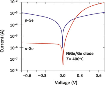
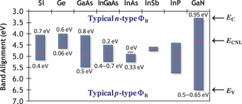
In general, for the application of MOSFET S/D ohmic contacts, Fermi-level pinning is undesirable since it takes away the ability to use metal work functions to tune to the barrier height. However, in the case of Ge, the Fermi level pins close to the valence band, which causes most metals to form a negative barrier to p-Ge, making ohmic contact formation extremely simple since there is no barrier for the majority carriers (Figure 2).Reference Pethe20 Similarly, the InAs Fermi level pins within the conduction band, which simplifies the formation of ohmic contacts to n-InAs. However, simplifying ohmic contacts for p-type typically means complicating ohmic contacts for n-type, and vice versa, since the barrier height may now be even larger than the entire bandgap. Figure 3 summarizes the E CNL and typical n-type and p-type Schottky barrier heights for a range of semiconductors.
Measured current-voltage characteristics of NiGe/Ge Schottky diodes on n-type and p-type Ge.Reference Pethe20 Rectifying characteristics are observed on n-type, and ohmic characteristics are observed on lightly doped p-type, confirming Fermi-level pinning within the valence band edge.

Band diagram information (E C [conduction band energy], E V [valence band energy], and E CNL [charge neutrality level]) for high mobility semiconductor materials, with E CNL indicated by the purple line. Numbers near E C represent typical pinned n-type Schottky barrier height ΦBN, and numbers near E V represent typical pinned p-type Schottky ΦBP.

Effective Barrier height tuning of metal/Ge and metal/III–V junctions
Depinning the Fermi levels
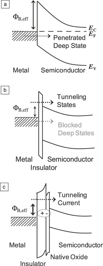
For the application of high mobility MOSFET S/D contacts, we need a near zero barrier height for minimal contact resistance, so the strong metal/semiconductor Fermi-level pinning needs to be reduced. Connelly et al.Reference Connelly, Faulkner, Grupp and Harris13 first depinned the metal/Si Fermi level by inserting an ultrathin silicon nitride (Si3N4) in between the metal and Si. In accordance with the MIGS theory, the ultrathin insulator physically separates the two materials, allowing the metal electron wave function to be attenuated in the insulator prior to penetrating the semiconductor. The attenuated metal states result in fewer charges available to drive E F toward E CNL, as shown in Figure 4. After depinning the Fermi level, the metal work function ΦM can then be used to tune the effective barrier height. For n-type ohmic contacts, metals with a low ΦM near the semiconductor conduction band should result in a near zero barrier height. For p-type ohmic contacts, metals with a high ΦM near the semiconductor valence band would be desirable.
(a) Schematic band diagram of a pinned Fermi level. The metal and semiconductor are in direct contact, allowing the tail of the metal electron wave function to decay into the semiconductor bandgap, creating metal-induced gap states that pin the Fermi level. (b) Metal/semiconductor Fermi-level depinning, where with an insulator, the metal wave function is attenuated in the gap states. (c) Schematic band diagram of a shift in the metal/semiconductor Fermi-level pinning by the formation of an electronic dielectric dipole.
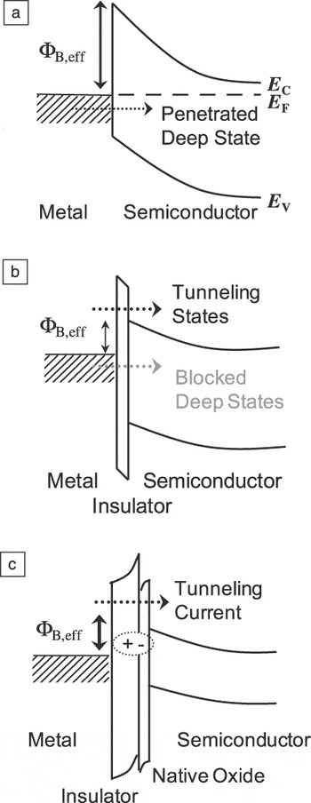
More recently, Coss et al.Reference Coss, Loh, Oh, Smith, Smith, Adhikari, Sassman, Parthasarathy, Barnett, Majhi, Wallace, Kim and Jammy21 used AlOx and LaOx to reduce the metal/Si barrier height to ΦBN ≤ 0.1 eV and ΦBP ≤ 0.2 eV, but the authors cited electronic dipole formation as the underlying mechanism, where in accordance with the bond polarization theory, an electronic dielectric dipole (ΦDipole) is created between the insulator and the semiconductor native oxide, inducing a barrier shift so ΦBN = ΦM + ΦDipole – χS. This dipole can be visualized as modifying the effective metal work function (ΦM,eff) and the interface specific region (Figure 4c), where for a given semiconductor, the magnitude of the dipole effect depends mainly on the insulator material. In this case, the metal work function ΦM needed for an ohmic contact would depend on the dipole magnitude.
Nevertheless, regardless of the underlying mechanism, the use of a thin insulator inserted in between the metal and semiconductor has been shown to be generally applicable to Ge and III–V semiconductors in reducing the effective electrical barrier height (ΦB,eff). Due to the absence of a model that accurately models the metal-thin insulator-semiconductor (MIS) structure, the term ΦB,eff is used to represent the overall electrical behavior of the MIS structure, modeled as a simple metal-semiconductor.
MIS contact to Ge
The MIS contact structure on both n-type and p-type Ge has been studied by several groupsReference Lieten, Degroote, Kuijk and Borghs22–Reference Kobayashi, Kinoshita, Saraswat and Wong24 using a variety of dielectrics ranging from Ge3N4 to AlOx. The application of the MIS contact appears to be generally applicable to various dielectrics, where the minimum achievable ΦB,eff can depend on both the metal and dielectric materials. It should be noted that these MIS contacts have been made on low doped substrates to minimize the tunneling current through the barrier and to emphasize the thermionic emission current over the barrier. This allows for a more accurate extraction of the barrier height and highlights the effect of changes in ΦB,eff. However, as a result, these contacts do not demonstrate extremely low contact resistances, and, in some cases, contact resistance is not even measured.
Lieten et al.Reference Lieten, Degroote, Kuijk and Borghs22 demonstrated the first MIS contact using a thin Ge3N4 layer to form an ohmic n-Ge contact and a rectifying p-Ge contact. Following the nitridation technique used by Connelly et al.Reference Connelly, Faulkner, Grupp and Harris13 on Si, the authors exposed Ge(001) and Ge(111) to nitrogen plasma in UHV at temperatures between 550–600°C to form both amorphous and (poly)crystalline Ge3N4 with a thickness of 0.7 nm. Metal was deposited immediately following the nitridation to suppress oxide formation, and no post deposition annealing was performed. Schottky barrier control samples were fabricated together.
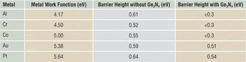
In contrast to the rectifying behavior of the control samples without Ge3N4, the current conduction through n-Ge samples with Ge3N4 was found to be ohmic for low work function metals Al (4.1 eV), Cr (4.5 eV), and Co (5.0 eV). For higher work function metals Au (5.4 eV) and Pt (5.6 eV), the current remained rectifying. This difference is promising for MIS contacts, because it indicates a sufficient reduction in the Fermi-level pinning to allow barrier height tuning through the metal work function. However, it should be noted that that the surface is not completely unpinned because ΦB,eff ≠ ΦM – χS. Table I summarizes the changes in the ΦB,eff with metal work function. Through this, Ge3N4 is shown to have a twofold benefit: (1) it passivates the dangling bonds of Ge for a low trap density at the Ge3N4/Ge interface, and (2) it has fewer surface states than Ge or effectively a larger pinning factor S.
Summary of effective barrier heights calculated from current-voltage (I-V) measurements for several metal work functions with and without an ultrathin 0.7 nm Ge3N4 dielectric.Reference Lieten, Degroote, Kuijk and Borghs22

In cases where no barrier was observed, the barrier height is estimated to be less than 0.3 eV.
Next, Nishimura et al.Reference Nishimura, Kita and Toriumi23 explored the use of thin oxides rather than nitrides for the MIS contact on n-type and p-type Ge(100) substrates, studied the effect of oxide thickness on barrier height, and successfully fabricated a Ge SB-FET. For contact fabrication, after native oxide removal, GeOx and AlOx were radio frequency sputtered at room temperature and then annealed at 400°C in N2.
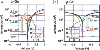
From the current-voltage electrical characterization shown in Figure 5, as the oxide thicknesses is increased from 0 to 2.2 nm, n-Ge diode behavior was transformed from rectifying to ohmic, while p-Ge diode behavior was transformed from ohmic to rectifying. As expected, the majority of the change is seen through the reverse-biased current, since carriers moving from metal to semiconductor are typically more affected by the barrier height than carriers moving from semiconductor to metal. It is important to note that without a reduction in ΦB,eff, the reverse current of the n-Ge MIS contact would not increase with oxide thickness. For the p-Ge MIS contact, the reverse current is interestingly asymmetrically suppressed by the oxide, which differs from the typical tunneling-limited current behavior that would reduce the current in both forward and reverse biases. This is due to the Fermi-level pinning of Ge close to the valence band, whereby most metals form ohmic contacts and a low Schottky barrier to p-Ge. However, after use of the oxide to depin the Fermi level, rectifying behavior can be achieved.
Current-voltage characteristics for Al/GeOx/Ge diodes.Reference Nishimura, Kita and Toriumi23 The effect of varying the GeOx thickness is shown in different curves, with the thickness indicated in nm. (a) For n-Ge, the reverse bias current increases with GeOx thickness, indicating a reduction of the barrier height. The inset shows the current-voltage curve for a GeOx thickness of 2.2 nm on a linear scale, emphasizing the achieved ohmic behavior. (b) For p-Ge, the current is asymmetrically suppressed by the oxide, indicating a depinned Fermi level. The inset shows the current-voltage on a linear scale for a GeOx thickness of 1.6 nm, demonstrating rectifying behavior. Reprinted with permission from Reference 23. ©2008, The Japan Society of Applied Physics.

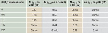
The change of barrier height with oxide thickness summarized in Table II supports the MIGS model, where the presence of the oxide suppresses the penetration of the metal electron wave function tail into the Ge. However, the roughly same ΦB,eff of 0.45 eV extracted for Al (ΦM = 4.1 eV) and Au (ΦM = 5.1 eV) despite a 1.0 eV difference in metal work function again suggests that Fermi-level pinning is just reduced, not removed. Furthermore, a ΦB,eff of 0.44–0.46 eV was found for both n-type and p-type Ge, where if there was true Fermi-level depinnining, the barrier heights should add up to be the bandgap (ΦBN + ΦBP = E g).
Summary of effective barrier heights (ϕB, eff) for Al (ΦM = 4.1 eV) and Au (ΦM = 5.1 eV) metal-insulator-semiconductor contacts for varying thicknesses of GeOx.Reference Nishimura, Kita and Toriumi23

Ohmic denotes cases where the on/off current ratio at ± 1V is less than 10.
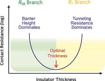
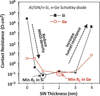
Kobayashi et al.Reference Kobayashi, Kinoshita, Saraswat and Wong24 further explored the MIS structure though the use of a thin radio frequency sputtered silicon nitride (SiN) layer and reported the lowest barrier height of 0.05 eV on Er/SiN/Ge, reduced from the Er/Ge Schottky barrier of 0.45 eV. In addition to ΦB,eff measurements, the contact resistance (R CO) as a function of the insulator thickness (t INS) was studied, where for Al/SiN/Ge, the minimum R CO was found for a dielectric thickness of 2 nm. Figure 6 depicts the modeling of R CO as two resistances in series: (1) R T, a tunneling resistance through the insulator, and (2) R SB, a resistance associated with the barrier. At t INS = 0 with no insulator present, the highly pinned Schottky barrier causes R CO to be dominated by R SB. Once a thin insulator is inserted and ΦB,eff begins to reduce, then R SB and thus R CO also begin to decrease. However, as t INS is further increased, the current through the MIS eventually becomes tunneling limited, whereby the increasing R T starts to dominate R CO. The overall R CO versus t INS curve (Figure 7) is a tradeoff between reduced ΦB,eff and increased R T, where there exists an optimal t INS for minimal R CO.
Schematic of contact resistance, R CO, versus insulator thickness, t INS. There exists an optimal insulator thickness for minimal contact resistance, which arises from the tradeoff between a reduced barrier (R SB branch) and an increased tunneling resistance (R T branch).

Measured contact resistance R CO versus SiN thickness t INS for the Al/SiN/Ge metal-insulator-semiconductor diode.Reference Kobayashi, Kinoshita, Saraswat and Wong24 The minimum R CO occurs at 2 nm. Reprinted with permission from Reference 24. ©2008, American Institute of Physics.

Through these various examples of Ge contacts, it is demonstrated that the MIS contact structure has great flexibility, where there are many more possible metal and dielectric combinations. As Kobayashi et al.Reference Kobayashi, Kinoshita, Saraswat and Wong24 showed, the optimal dielectric thickness changes with both materials. The chosen dielectric affects both how much the ΦB,eff is reduced, which changes the shape of the R SB branch, and determines the band offset that will shift the R T branch left or right.
MIS contact to III–V semiconductors
Hu et al.Reference Hu, Guan, Saraswat and Wong25, Reference Hu, Saraswat and Wong26 have investigated the MIS contact structure on III–V semiconductors by using sputtered SiN and atomic layer deposition (ALD) Al2O3 on both GaAs and In0.53Ga0.47As. GaAs was primarily studied due to its large bandgap of 1.42 eV, which facilitates ΦB,eff extraction, and also as a baseline III–V material to develop a contact structure that can be extended to other more technologically relevant III–V materials. For the MIS contact study, as in the Ge case, a lightly doped GaAs substrate with a doping density of 2 × 1016 cm–3 was used to emphasize the thermionic emission current and changes in ΦB,eff.
For GaAs, the native oxide forms a low density, high surface states interface that causes strong Fermi-level pinning, and so great care needs to be taken in minimizing the formation of native oxide during contact fabrication. Native oxide removal using dilute HCl followed by sulfur passivation in ammonia sulfide (NH4)2S has been shown to terminate with Ga–S and As–S bonding, which helps prevent further oxidation.Reference Chen, Sun and Nishi27 For the MIS contact, immediately following sulfur passivation, amorphous SiN was deposited at 200°C through wafer biased radio frequency sputtering from a stochiometric Si3N4 target. The wafer bias and heat are critical, since without the two, the resulting SiN film is less dense and uniform and does not reduce the Fermi-level pinning. For the aluminum oxide samples, the ALD Al2O3 was deposited using trimethylaluminum (TMA) and H2O precursors at 300°C. It is also crucial to start the ALD process with the TMA pulse, which is necessary for the “self-cleaning” effect on the III–V native oxide, where As2O3 and GaO are removed through a ligand exchange process.Reference Hinkle, Sonnet, Vogel, McDonnell, Hughes, Milojevic, Lee, Aguirre-Tostado, Choi, Kim, Kim and Wallace28
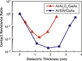
Figure 8 illustrates the same contact resistance and dielectric thickness tradeoff also found in the Ge MIS contacts. The existence of a minimum contact resistance for a non-zero dielectric thickness confirms the reduction in barrier height. In comparing the dielectrics, it is clear that SiN is the better option of the two, and suggests that it may be possible to achieve even lower contact resistance with the use of alternative dielectrics. It also highlights the large effect the conduction band (∆E C) and valence band (∆E V) offsets have on the tunneling resistance R T in the MIS structure for n-type and p-type semiconductors. The band offsets of Al2O3 (∆E C = 2.75 eV) and SiN (∆E C = 1.5 eV) to GaAs differ by 1.25 eV, but the intrinsic exponential dependence of the tunneling current on the potential barrier amplifies this difference. The effect of the dielectric on R SB depends on the amount of reduction in ΦB,eff, so the ideal dielectric would be one that has a larger ∆ΦB,eff and zero or even negative band offset (∆E C for n-type and ∆E V for p-type) to reduce the tunneling penalty on R C.
Comparison of the contact resistance, R CO, versus insulator thickness, t INS, tradeoff for SiN and Al2O3, where the contact resistance ratios are taken relative to the Schottky diode case. SiN appears to be the better candidate for contact applications due to its lower ∆E C of 1.5 eV, which is reflected in the reduced tunneling resistance at a given insulator thickness. Reprinted with permission from Reference 26. ©2010, American Institute of Physics.

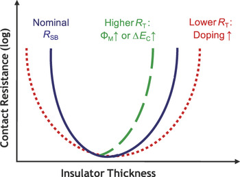
Through varying ΦM from Y (ΦM = 3.1eV) to W (ΦM = 4.5eV) on the MIS contact using SiN, the authors find that the optimal thickness is inversely dependent upon the metal work function. The lowest achievable contact resistance also has a dependence on ΦM that arises mainly from the band alignment of the metal with the dielectric, which affects the tunneling barrier from metal to semiconductor. In studying the effect of substrate doping, it was found that there is a slightly wider t SiN process window for higher doped substrates. The reasoning lies in the reduction of the depletion width with higher doping, which causes the Schottky barrier tip to become thinner. The R T curve effectively shifts toward the left, and the R SB curve shifts toward the right due to increased tunneling current from a thinner tunneling barrier. Figure 9 summarizes how changing the various material parameters affects the overall R CO versus t INS tradeoff. For an ultralow contact resistance, a combination of high electrically active doping and low effective barrier heights is necessary.
Schematic of contact resistance, R CO, versus insulator thickness, t INS. The effect of different metals, dielectrics, and substrates on the tradeoff between R CO and insulator thickness is shown, where R T is the tunneling resistance through the insulator, and R SB is the barrier-related resistance. The figure shows that the tunneling resistance will be suppressed for higher substrate doping, smaller band offset between dielectric and substrates, and lower metal work functions (ΦM).

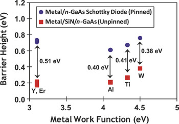
As mentioned earlier in this article, the mechanism of this observed reduction in barrier height is not yet fully understood. MIGS has been cited as a reason, however, MIGS has an asymptotic charge decay length λ of 3Å for GaAs and 4Å for Ge, which implies that for any sufficiently thick dielectric, all the MIGS should be blocked, and the Fermi level should be depinned. However, complete Fermi-level depinning is not observed in both Ge and GaAs, as the barrier heights are not completely tuned by the metal work function. On the other hand, the presence of an electronic dipole formed based on differences in oxygen density is also cited as a possibility. Figure 10 summarizes the measured changes in the ΦB,eff of Schottky diodes with varying ΦM, with and without the use of SiN. In particular, for a metal/SiN/GaAs contact, the approximately constant reduction of ΦB,eff by roughly 0.4 eV for all samples regardless of ΦM suggests the presence of a dielectric dipole with a magnitude between 0.4 to 0.5 eV. Nonetheless, for a more thorough understanding, an even wider range of dielectrics and metals needs to be studied, and Hu et al.Reference Hu, Saraswat and Wong26 suggest a series of experiments that could be used to help determine the underlying mechanism.
Effective barrier height versus metal work function for Schottky diodes and metal-insulator-semiconductor contacts. The roughly parallel shift in ΦB,eff independent of ΦM confirms the dielectric dipole induced shift of roughly 0.4 to 0.5 eV. Reprinted with permission from Reference 26. ©2010, American Institute of Physics.

Summary
The metal-insulator-semiconductor (MIS) contact structure has demonstrated great promise on Si, Ge, and III–V materials through the use of a thin dielectric to reduce the effective electrical barrier height and contact resistance of a pure metal-semiconductor contact. For Ge, this provides a possible solution to the low n-type Ge dopant solubility and allows for the fabrication of Schottky barrier source/drain transistors with barriers as low as 0.05 eV. For III–V semiconductors, the MIS contact allows for the use of a non-alloyed contact that is crucial for the scalability of III–V MOSFETs. Current demonstrations of the MIS contact have barriers as low as 0.18 eV, but this can most likely be further reduced with the use of different combinations of materials. As discussed, the overall minimum achievable contact resistance and barrier height has a strong dependence on the metal, dielectric material, dielectric thickness, and substrate doping. For a low contact resistance, both heavy doping and low barrier heights are required. The dielectric remains the most critical factor in tuning the resulting effective barrier height, where the pinning factor S, oxygen density, and band offsets are all key parameters. This offers great flexibility in the design of the MIS contact, where there is still much more that can be studied.
Acknowledgments
This work is supported, in part, by the Focus Center Research Program (FCRP) (MSD), Intel Corporation, and NSF (ECS-0501096). J. Hu is additionally supported by the Intel PhD Fellowship, Stanford Graduate Fellowship, and the National Defense Science and Engineering Graduate Fellowship.