I. INTRODUCTION
Radiometry has become an established technique not only for radio astronomy, remote sensing, and environmental observation, but also for passive millimeter-wave (PMMW) imaging applications, such as security portals and stand-off detection. Employing square-law detection and assuming a linear behavior of the amplifier cascade, a straightforward two point calibration (Y method) might be sufficient [Reference Ulaby, Moore and Fung1]. However especially the astronomical, geophysical, and meteorological scientific applications depend on an accurate absolute radiometric calibration of the instruments. While ground-based instruments can afford time, complexity and effort of extensive calibration routines, mobile systems like satellites are limited in their payload and duty cycle time.
Recently, novel calibration techniques with internal active loads are being investigated to minimize orbital maneuvers and moving mechanical parts for the calibration with external reference targets [2]. Apart from compact size, low weight and minimum power consumption, active loads allow presenting multiple references to the radiometer, when combined with an appropriate switching front-end [Reference Weissbrodt3]. This minimizes interpolation errors and accounts for non-linearity of the radiometer. In addition, fast switching front-ends increase the repetition rate and shorten the calibration intervals, which further improve the accuracy and the duty cycle. Although most of today's PMMW imaging radiometers in security screening systems omit an absolute calibration because its time effort is in contrast to the imperative high scanning speed (ideally real-time), switching calibration front-ends (SCFEs) might even prove to capture a new market. In this work, a highly compact SCFE monolithic integrated circuit (MMIC) with integrated active “cold” and “hot” loads (ACL, AHL), a passive “warm” load, and two input channels was developed, manufactured, and characterized [Reference Diebold, Kallfass and Weissbrodt4]. The two active loads were previously built as stand-alone devices for a detailed analysis and were then integrated with single-pole-five-throw (SP5T) field effect transistor (FET) switch on a single MMIC. Through the combination of these two crucial first radiometer stages in one device, the losses between the reference loads and the switch can be minimized because waveguide transitions are not required and transmission line lengths can be significantly reduced.
II. METAMORPHIC HIGH ELECTRON MOBILITY TRANSISTOR (mHEMT) TECHNOLOGY
The challenge of ACL design is to obtain the lowest achievable noise temperature at the gate of a transistor without physical cooling. Ideally, the hot and cold reference loads encompass the noise temperature range of the expected targets. For astrophysical instruments, the lower limit can reach down close to the noise temperature of the cosmic background radiation. Typical scene temperatures in radiometry range from 100 to 335 K [5]. While conventional cold loads as liquid nitrogen (LN) exhibit a temperature of 77 K, published ACL noise temperatures range from 50 K at 1.4 GHz to 155 K between 87 and 110 GHz (see Table 1). Table 1 also shows an overview of the utilized transistor technologies for previous ACL designs. While InP HEMTs would be the technology of choice for lowest achievable noise temperature [Reference Dunleavy, Smith, Lardizabal, Fejzuli and Roeder7], GaAs mHEMTs are a lower cost alternative with equivalent performance [Reference Buhles and Lardizabal8, Reference Weisbrodt, Tessmann, Schlechtweg, Kallfass and Ambacher13]. For this work, Fraunhofer IAFs in-house 50 nm mHEMT process was chosen. Technological details can be found in [Reference Leuther14]. Based on this technology, state-of-the-art low-noise amplifiers (LNAs) with less than 2 dB noise figure have been demonstrated in W-band [Reference Leuther15]. In addition to the active device, this technology allows to implement passive structures such as metal–insulator–metal (MIM) capacitors, NiCr thin-film resistors and airbridges, as well as grounded coplanar waveguide (GCPW) transmission lines. With these components, complex matching networks can be designed on chip and different circuits can be integrated on a single MMIC.
State-of-the-art of ACLs realized in different technologies and at different frequencies.

III. CIRCUIT DESIGN
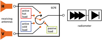
The principle operation mode of the SCFE is demonstrated in Fig. 1. A SP5T switch allows routing the signal from five different sources to a common output port. While two branches are connected to two input ports (e.g. two orthogonal polarized receiving antennas), the three remaining branches are connected to active and passive loads within the same MMIC. The output of the SCFE will be connected to the first stage LNA of a radiometer system.
Principle operation mode of SCFE and example of application in a polarimetric radiometer system.

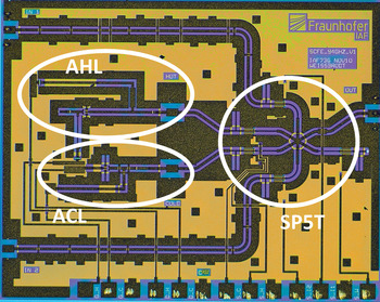
Figure 2 shows a chip photograph of the manufactured MMIC with the dimensions 2 × 2.5 mm2. The transmission lines from the five signal sources and the output port all intersect at a common star point. At λ/4 distance of this point FETs are placed in shunt to the signal lines. The channel conductance of the transistors can be controlled by the applied gate voltage. For above-threshold bias conditions, the transistor shortens the signal line to ground and the short circuit is transformed by the λ/4-line to an open circuit at the star point, isolating this specific branch. For sub-threshold bias conditions the FET channel is pinched-off, its parasitic capacitance is compensated by a shorted stub in close vicinity of the FET and the signal is routed to the output [Reference Kallfass, Diebold, Massler, Koch, Seelmann-Eggebert and Leuther16]. Since the function of this type of switches is not dependent on the performance of the FET itself, but on the passive circuits, the repeatability and stability of the switching operation is warranted. The switching process involves no mechanics and is not subject to degradation like today's microelectromechnical system (MEMS)-based switches still are. Moreover, the switching rate is merely limited by the transistor speed. These facts are crucial for fast, continuous and reliable switching to calibration loads.
Chip photograph of W-band SCFE MMIC with integrated active loads (2 × 2.5 mm2).

While the matched passive load at one of the internal signal paths is realized by terminating the accordant transmission line with a 50 Ω NiCr resistor, the active loads were simulated and designed, using IAFs proprietary ADS model libraries. The transistor model features the prediction of noise parameters as a function of applied bias voltage [Reference Seelmann-Eggebert, Schaefer, Leuther and Massler17], which was used to achieve the desired noise temperature and input return loss. To realize the AHL (upper internal circuit in Fig. 2), the SP5T is connected to the drain of a transistor via a matching network, while on the gate side of this transistor a second passive network transforms the 50 Ω NiCr termination to the optimum impedance for excess noise. For the ACL (lower internal circuit in Fig. 2), the transistor is connected with its gate to the SP5T and the drain is terminated with a 50 Ω NiCr resistor. Here, the matching networks on gate and drain side, as well as the feedback of the parallel source lines are optimized to operate the transistor at the optimum noise impedance, so the ACL can deliver its minimum noise temperature. The transistors in both active loads are realized with a gate length of 2 × 15 µm. To verify the simulation approach, especially the noise prediction, the active loads were previously manufactured as stand-alone devices [Reference Weisbrodt, Tessmann, Schlechtweg, Kallfass and Ambacher13]. Except for the DC-routing, the cores of the active loads are identical to the ones seen in Fig. 2. The two 1 × 1 mm2 MMICs were first characterized on-wafer and then mounted into split-block packages for further analysis of the noise sensitivity to external physical temperature changes.
IV. MEASUREMENT SETUPS
A) S-parameter measurements
The isolation and the insertion loss of the SCFE and the return loss of all MMICs were measured with an Agilent PNA series vector network analyzer and Cascade Microtech probes. Furthermore, all passive and active components of the noise measurement setup described in the next subsection were thoroughly characterized to allow the investigation of possible reflections between the stages and to calculate the influence of mismatched impedances. The S-parameters of the RF-probe used for the noise measurements were calculated with Cascade Microtech's WinCal software, based on measurements of calibration substrates.
B) On-wafer noise measurements
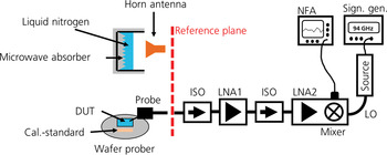
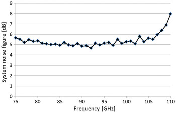
For the noise temperature characterization of the reference loads a dedicated hot–cold measurement setup with the possibility of on-wafer one port measurements was established. A schematic diagram of the setup can be seen in Fig. 3. The reference plane for the hot–cold calibration with a corrugated horn antenna and microwave absorber at 398 and 77 K temperature is behind the RF-probe, which is mounted on a wafer probe station. To cool down the absorber, LN was used. Since the probe is not within the calibration loop, the resistive part of its loss adds noise to the measured noise temperature of the device under test (DUT). This additional noise is taken into account and subtracted from the result after measurement. The receiver consists of a LNA module with 20 dB small-signal gain and a receiver module containing an integrated LNA-mixer-MMIC with a conversion gain of approximately 10 dB. To minimize the influence of noise reflections, isolators were placed at critical stages. The return losses of the first stage isolator and the on-wafer measurement probe are both around 20 dB and the return loss of the horn antenna lies even well above 20 dB. Since this is crucial for accurate measurement of the DUT with the Y-method, the degradation of the system noise figure due to a lossy first stage is accepted. The system noise figure of the measurement setup at the reference plane is shown in Fig. 4. It is around 5 dB in the frequency range of 81–102 GHz. It should be noted that this slightly worsens if referred to the reference plane on chip, due to the mentioned losses of the probe.
On-wafer one-port noise measurement setup with hot–cold calibration method.

System noise figure of the measurement system at the reference plane.

C) Temperature chamber measurements
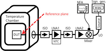
While the noise temperature of passive loads has a linear relation to its physical temperature, investigations in [Reference Sobjaerg, Skou and Balling10, Reference de la Jarrige, Escotte, Goutoule, Gonneau and Rayssac11] have shown, that ACLs are less sensitive to temperature variations than passive loads. To analyze the temperature dependence of the ACL design used in the presented switching calibration MMIC, a packaged stand-alone ACL [Reference Weisbrodt, Tessmann, Schlechtweg, Kallfass and Ambacher13] was characterized in a temperature chamber. The ACL module was placed into a WEISS WKL series climate and temperature test chamber and connected with a WR-10 waveguide to the measurement receiver outside the chamber (see Fig. 5). The measurement setup was calibrated at the reference plane at the ACL module before and after the test series. To ensure a stable operation of the receiver and to minimize the influence of thermal conduction through the waveguide, a fan was placed at the front-end and a thermistor (NTC) was attached to the first stage LNA, monitoring its temperature. To avoid condensation inside the ACL module, the temperature ramp was run from cold to hot. The temperature was increased from −40 to +80°C in steps of 10°C. Since the ACL is not an amplifying element and has negligible power dissipation, it can be assumed that after an appropriate time, the temperature of the module is equal to the temperature set inside the test chamber.
Temperature chamber measurement setup.

V. SIMULATION AND RESULTS
A) Insertion loss and isolation of the SP5T
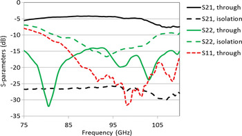
Since the two input channels are designed symmetrically, only the upper branch was characterized. In Fig. 6S-parameter measurement results are shown, where port 1 is the input port and port 2 is the output port. In “through” position all branches are closed (V sw = +0.1 V), except for the upper input signal path (V sw = −0.5 V). An insertion loss between −4 and −5 dB is measured within the bandwidth of 80 to 100 GHz. To enable on-wafer measurements, it was necessary to place the RF-pads on opposite sides of the MMIC and the DC-pads on one of the remaining sides, which resulted in a considerable input line length. While subsequent designs – optimized for packaging – will not have this constraint, this caused a substantial additional loss to the insertion loss on the actual design. Furthermore, it is not possible directly to measure the S-parameters of the internal switch branches, due to the integrated design. To estimate the switch loss on the path to the internal active loads, the loss of the line length difference of 1700 µm between internal and input paths was simulated to be −0.7 dB. This results in an estimated insertion loss of −3.3 to −4.3 dB for the two internal paths to the active loads. To measure the isolation of the SCFE, the output port is routed to the internal matched load and S-parameters are measured at the same ports as above. An isolation of more than −25 dB is measured within the entire W-band. Furthermore, the input return loss is very good in all switching states of the SCFE.
S-parameters between input port 1 and output port for switch position to input port 1 (through) and to internal matched load (isolation).

B) Return loss and noise temperatures of active loads and SCFE
1) ACTIVE COLD LOAD
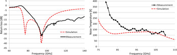
It is crucial to ensure that the loads are sufficiently matched to the impedance of the switch to avoid reflecting noise power. Since it is not possible to characterize the input return loss of the loads once they are integrated on the SCFE, identical active load designs were measured as stand-alone devices separately. This allowed furthermore verifying the simulation approach of the active loads. In Figs 7 and 8, the simulation results (dashed curves) are compared with the measurement results (solid curves) for return loss and noise temperature, respectively. The ACL has a notable input return loss of −30 dB at its center frequency of 94 GHz and is fairly well matched for frequencies above 80 GHz. Furthermore, it exhibits a noise temperature of 150 K around its center frequency, which rapidly increases for frequencies below 85 GHz. This is obviously due to the degrading input return loss.
Comparison of simulated and measured input return loss of the ACL MMIC (left) and noise temperature (right).

Comparison of simulated and measured input return loss of the AHL MMIC (left) and noise temperature (right).

2) ACTIVE HOT LOAD
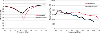
The AHL achieves an input return loss of −15 dB at its center frequency and still below −5 dB from 60 to 115 GHz and agrees very well with the simulated values. However, the provided noise temperature decreases faster than predicted towards the higher frequencies. Nevertheless, the AHL exhibits a noise temperature of 2800 K at the center frequency which permits a high enough excess noise ratio (ENR) to be suitable for hot–cold calibration.
3) SWITCHING CALIBRATION FRONT-END
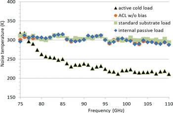
For the characterization of the cold reference on the SCFE, the SP5T switch was set to the accordant position. The ACL was biased with a gate voltage of +0.1 V and a drain voltage of +0.7 V, resulting in a normalized drain current of 173 mA/mm at which the lowest noise temperature was achieved. Unlike the AHL, the ACL is very insensitive to bias variations. The difference of the highest and the lowest achievable noise temperature with extreme bias conditions is less than 20 K within the entire operation bandwidth. For frequencies above 90 GHz, a mean noise temperature of 220 K was achieved (Fig. 9). Compared with the measured temperature of 150 K of the stand-alone ACL in the previous subsection, an increase of only 70 K is due to the losses of the SP5T switch. Transforming equation (1) for temperature change due to passive lossy devices from [Reference Skou18] into (2) and inserting T 0 = 298 K for the ambient temperature, T 1 = 150 K for the ACL temperature, and T 2 = 220 K for the SCFE temperature results in a calculated loss L dB of the SP5T of approximately 3 dB. This value, based on measured results is even below the simulated losses in Section V(A)).
 $$T_2=T_1 \times L_{lin}+T_0 \lpar 1 - L_{lin}\rpar \comma \;$$
 $$\hskip-13ptL_{dB}=10 \times \log _{10} \left({\displaystyle{{T_2 - T_0 } \over {T_1 - T_0 }}} \right).$$
Noise temperatures in switch positions “ACL” and “passive load”, compared to standard substrate load and ACL w/o bias.

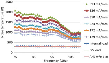
The hot reference on the SCFE was characterized accordingly. In contrast to the ACL, however, it is possible to achieve different levels of noise temperature as a function of transistor biasing. Again, the originally higher noise levels of the stand-alone AHL are reduced by losses of the SP5T, but noise temperatures between 890 and 1750 K at 94 GHz were measured at the output of the SCFE (Fig. 10). Without bias, the AHL exhibits a noise temperature similar to the measured standard substrate and the internal passive load at an ambient temperature. All three curves can be seen in Fig. 10 around 298 K, but are congruent at this scaling. The variable noise temperature allows operating the AHL at different bias points in order to extend the number of reference loads above three, and to improve the calibration accuracy of a radiometer even more. There, however, remains the necessity to analyze the influence of biasing and of temperature changes on the stability of the AHL.
Noise temperatures in switch position “AHL” at different AHL bias, compared to standard substrate load and AHL w/o bias.

The ideal case of encompassing the typical radiometry scene temperature range with internal active hot and cold references is challenging on the cold reference part. Especially, the losses of the SP5T cause a noticeable increase of noise temperature.
C) Temperature dependence of ACL module
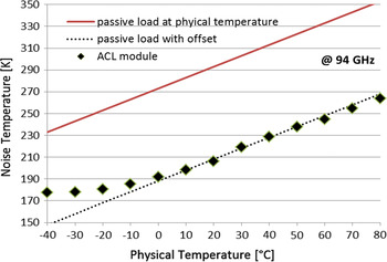
When characterizing the sensitivity of the ACL to external physical temperature changes, the entire W-band was measured at each temperature step. For clarity sake only the results at the center frequency are shown. However, it should be noted that since the performance of the ACL is frequency dependent, the sensitivity to temperature changes is as well. The solid line in Fig. 11 shows the noise temperature, which a passive matched load would exhibit at the accordant physical temperature. The slope of the curve is 1 K/°C. For a better comparison to the sensitivity of the ACL, an offset was subtracted from this curve which corresponds to the difference between a passive load and the presented ACL at ambient temperature. In comparison to the dashed offset curve it can be observed that for physical temperatures below ambient the ACL is less sensitive to temperature changes than a passive load, while for temperatures above ambient a similar behavior as for a passive load can be observed. In the application scenario of an ACL as a calibration reference, however, such extreme temperature changes are not expected, since these systems are typically very accurately temperature stabilized. However, it is noteworthy, that the noise temperature of an ACL – being an active device – does not increase more than a passive load, when being heated.
Measured noise temperature of ACL module at different physical temperatures, compared to the theoretical value of a passive matched load.

VI. CONCLUSION
A highly integrated switching front-end with multiple active and passive loads was developed and tested, to be analyzed and used in novel calibration techniques. It is the first published device of this kind and an accordant patent was granted [Reference Diebold, Kallfass and Weissbrodt4]. A temperature range from 220 to 1750 K at the center frequency of 94 GHz was achieved at the output of the SCFE. While a setup of separate modules as in [Reference Weissbrodt3], with a −4.3 dB switch loss and an ACL module noise temperature of 220 K [Reference Weisbrodt, Tessmann, Schlechtweg, Kallfass and Ambacher13] would result in a temperature of 270 K at the output of the switch, the SCFE exhibits a noise temperature of 220 K at its output. Packaging the SCFE will add an additional loss of approximately 1 dB, but will still show superior performance while reducing the size. Subsequent developments promise an even more compact and low-loss device, since it is not necessary to match to 50 Ω at the internal interfaces between the switch and the loads.
ACKNOWLEDGEMENTS
This work was supported by the German Federal Ministry of Defence (BMVg) and the Bundeswehr Technical Center for Information Technology and Electronics (WTD81). We express our gratitude to our colleagues at the IAF for their excellent contributions during epitaxial growth and wafer processing.
 Ernst Weissbrodt received the Dipl.-Ing. degree in Electrical Engineering and Information Technology from the Karlsruhe Institute of Technology (KIT), Germany, in 2007. During his studies he spent six months at the Alaska Satellite Facility, USA, where he supported the calibration campaign of the ALOS satellite. For his diploma thesis on the phase synchronization of the TanDEM-X satellites at the German Aerospace Center (DLR), he received the “ARGUS Award 2008” from EADS Defence Electronics, Germany. Since 2008, he has been with the Fraunhofer Institute for Applied Solid State Physics (IAF) in Freiburg, Germany, where he is working toward his doctoral degree. His research interests include the design of MMICs for applications in millimeter-wave radiometry.
 Michael Schlechtweg received his Dipl.-Ing. degree in Electrical Engineering from the Technical University Darmstadt in 1982, and the Dr.-Ing. degree from the University of Kassel in 1989. He joined the Fraunhofer Institute for Applied Solid State Physics in Freiburg, Germany, working on the design of millimeter-wave integrated circuits, and on non-linear characterization and modeling of active RF devices. In 1994, he became head of the simulation and modeling group at Fraunhofer IAF. Since 1996, he leads the RF devices and circuits department, focusing on the design and the characterization of devices and integrated circuits based on III–V compound semiconductors for RF applications, as well as the development of integrated circuits and modules for sensor and communication systems up to 600 GHz and above. Michael Schlechtweg received the Fraunhofer Prize in 1993, and the European Microwave Prize in 1998. He has co-authored about 200 scientific publications, and holds two patents.
 Oliver Ambacher received his Dipl.-Phys. and Dr. degrees with honors from the Ludwig-Maximilians and Technical University Munich, in 1989 and 1993, respectively, where he was involved in the deposition and characterization of amorphous silicon for solar cells. In 1992 he received a German Science Foundation Graduate Research Fellowship. In 1993, he joined the Walter Schottky Institute of the TU-Munich to investigate the epitaxial growth of group-III nitrides based heterostructures. 1998/99, he spent one year at Cornell University, Ithaca, NY, as an Alexander von Humboldt fellow. He became a professor of Nanotechnology and head of the Institute for Solid State Electronics located at the Technical University of Ilmenau in 2002. In 2004, he was elected as head of the new Center of Micro- and Nanotechnologies. Since 2007, he is the head of the Fraunhofer Institute of Applied Solid State Physics and Professor for Compound Microsystems in Freiburg, Germany.
 Ingmar Kallfass received the Dipl.-Ing. degree in Electrical Engineering from University of Stuttgart in 2000, and the Dr.-Ing. degree from the University of Ulm in 2005. In 2001, he worked as a visiting researcher at the National University of Ireland, Dublin. In 2002, he joined the department of Electron Devices and Circuits of University of Ulm as a teaching and research assistant. In 2005, he joined the Fraunhofer Institute for Applied Solid-State Physics with a focus on non-linear millimeter-wave integrated circuit design. From 2009 to 2012, he was a professor at the Karlsruhe Institute of Technology in the field of high-speed integrated circuits in a shared professorship with the Fraunhofer IAF in the frame of the German Excellence Initiative. Since 2013, he holds the newly established chair for Robust Power Semiconductor Systems at the University of Stuttgart as part of the Robert Bosch Center for Power Electronics.