

I. INTRODUCTION
Among high-temperature superconducting materials, the La2−xSrxCuO4 (LSCO) system is important to research on the superconductor physical mechanism and the application of the device because its superconductor transition temperature can be modified by varying the carrier concentration over a wide range. Therefore, there have been many research works on La2−xSrxCuO4 single crystal materials and high-quality films. The fabrication process of a high-quality thin film was one of the major research works for the application goal of this high-T c film (Cieplak et al., Reference Cieplak, Berkowski, Guha, Cheng, Vagelos, Rabinowitz, Wu, Trofimov and Lindenfeld1994; Liang et al., Reference Liang, Chen, Shi, Lu, Lu and Kear1995; Geerk et al., Reference Geerk, Zaitsev, Linker, Aidam, Schneider, Ratzel, Fromknecht, Scheerer, Reiner, Gaganidze and Schwab2001). After many years, the study of monolayer film has been moving toward maturity, and many research works have turned to building heterogeneous structures, such as the p–n junction (Xiang et al., Reference Xiang, Qu, Zhang, Lu, Zhou, Li and Li2007; Shi et al., Reference Shi, Zhao, Zhang and Zhang2008; Guo et al., Reference Guo, Guo, Lei, Chen, Tang, Li, Fu and Li2009; Chen et al., Reference Chen, Li, Zhang and Guo2010; Yin et al., Reference Yin, Ding, Wang, Xie, Yu and Li2010). Besides results on building a heterogeneous structure, recently also results on preparing bilayers or multilayer films using different doped LSCO materials and studying the interaction between the films were reported (Caviglia et al., Reference Caviglia, Gariglio, Reyren, Jaccard, Schneider, Gabay, Thiel, Hammerl, Mannhart and Triscone2008; Ueno et al., Reference Ueno, Nakamura, Shimotani, Ohtomo, Kimura, Nojima, Aoki, Iwasa and Kawasaki2008; Biscaras et al., Reference Biscaras, Bergeal, Kushwaha, Wolf, Rastogi, Budhani and Lesueur2010; Koren and Millo, Reference Koren and Millo2010; Rout and Budhani, Reference Rout and Budhani2010; Bollinger et al., Reference Bollinger, Dubuis, Yoon, Pavuna, Misewich and Božović2011). Yuli et al. (Reference Yuli, Asulin, Millo, Orgad, Iomin and Koren2008) reported the observation of a large T c enhancement in bilayers of the non-superconducting, heavily overdoped La1.65Sr0.35CuO4, and superconducting underdoped La1.88Sr0.12CuO4, in comparison with the bare film of the latter (Yuli et al., Reference Yuli, Asulin, Millo, Orgad, Iomin and Koren2008). Following a previous study by Yuli et al. (Reference Yuli, Asulin, Millo, Orgad, Iomin and Koren2008), results on LSCO films with different doping densities that can influence and tune each other due to a conventional proximity effect were reported (Koren and Millo, Reference Koren and Millo2009; Shapiro et al., Reference Shapiro, Shapiro and Atzmon2009). The result that thin films with different doping densities can influence each other is quite interesting, although the specific mechanism has not been particularly clear; these phenomena should be related to the transfer of carrier in the films.
In this paper, we studied the influence of the deposition parameters of the pulsed laser deposition technique (PLD) on the quality of LSCO films, and obtained an optimal process for fabricating LSCO films. Then the optimized parameters were used to fabricate La1.8Sr0.2CuO4/La1.9Sr0.1CuO4 bilayers. The electrical transport properties were characterized, and a rectifying behavior was observed, indicating potential applications of the LSCO bilayers in novel electronic devices.
II. EXPERIMENTAL
The La1.8Sr0.2CuO4 and La1.9Sr0.1CuO4 targets were prepared by the conventional solid-state reaction method. The targets were 3-mm ceramic discs of 30 mm diameter. The chemicals used for preparing the two LSCO targets were polycrystalline powders of La2O3, SrCO3, and CuO. Nominal compositions of the targets were weighed according to the expression La2−xSrxCuO4 with x = 0.1 and 0.2. Each polycrystalline powder of each target was first ground in an agate mortar for 1 h, and dried in a vacuum oven for 2 h. After that, it was pressed into a disc, then sintered at 750 °C for 6 h, and re-ground. Finally, it was pressed with a pressure of 18 MPa and sintered at 1100 °C for 12 h.
In the process of the LSCO thin-film preparation by PLD, the film deposition parameters were changed one at a time to study the effects of laser energy, oxygen atmosphere, substrate temperature, and target–substrate distance on the properties of the films. Under the optimal conditions, the La1.8Sr0.2CuO4/La1.9Sr0.1CuO4 bilayers were firstly deposited on a (001) SrTiO3 single-crystal substrate which was in turn cleaned and dried. And we used the concentrated HNO3 solution that has been diluted to ablate the top film, so the film step structure of two different components was fabricated at the surface and then the electrical transport properties were studied (Huang et al., Reference Huang, Liu, Wu, Jia, Xu and Zhao1999).
X-ray powder diffraction measurements were carried out on a Bruker AXS D8 DISCOVER X-ray diffractometer with Cu Kα radiation. The patterns were taken in the 2θ range from 10 to 80° at a speed of 0.02°/s. The morphology of the as-obtained samples was characterized on a Hitachi 4800 scanning electron microscope (FESEM). The electrical transport properties of bilayers were characterized with a low-temperature electrical measurement system composed of a multifunctional SourceMeter of Keithley 2400, a cooling system of liquid helium, and a Lakeshore 331 temperature controller.
III. RESULTS AND DISCUSSION
A. Characterization of targets
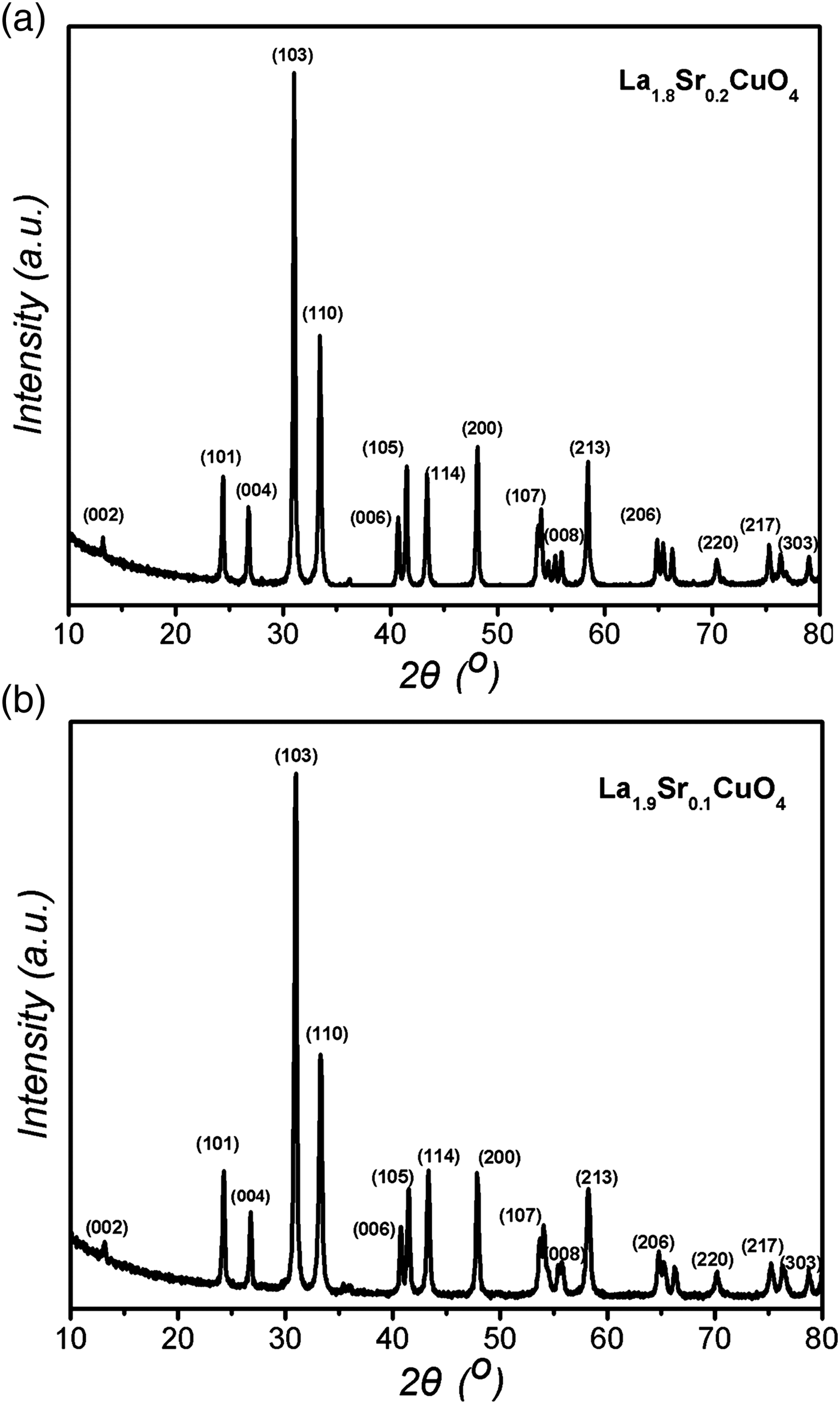
The two La1.8Sr0.2CuO4 and La1.9Sr0.1CuO4 targets were characterized by X-ray diffraction (XRD). The results indicate that the sintered samples with 1150 °C show all the peaks that belong to the different crystal planes of LSCO, while no other visible impurity peaks were detected as shown in Figures 1(a) and 1(b).
XRD patterns of targets: La1.8Sr0.2CuO4 (a) and La1.9Sr0.1CuO4 (b).

B. Preparation of thin films
The technological conditions for depositing the LSCO films are listed in Table I. Figure 2 shows the XRD patterns for La1.8Sr0.2CuO4 film under different oxygen atmospheres, while other conditions were kept unchanged. We can see that 30 Pa was the optimal parameter in which the film has a strong c-axis orientation growth that confirms a reliable quality without detectable impurity peaks, except those belonging to the (00 l) aligned LSCO film and the (001) oriented STO substrate.
XRD patterns of La1.8Sr0.2CuO4 thin films deposited at different oxygen atmospheres.
Technological parameters for deposition of La1.8Sr0.2CuO4 films by PLD.

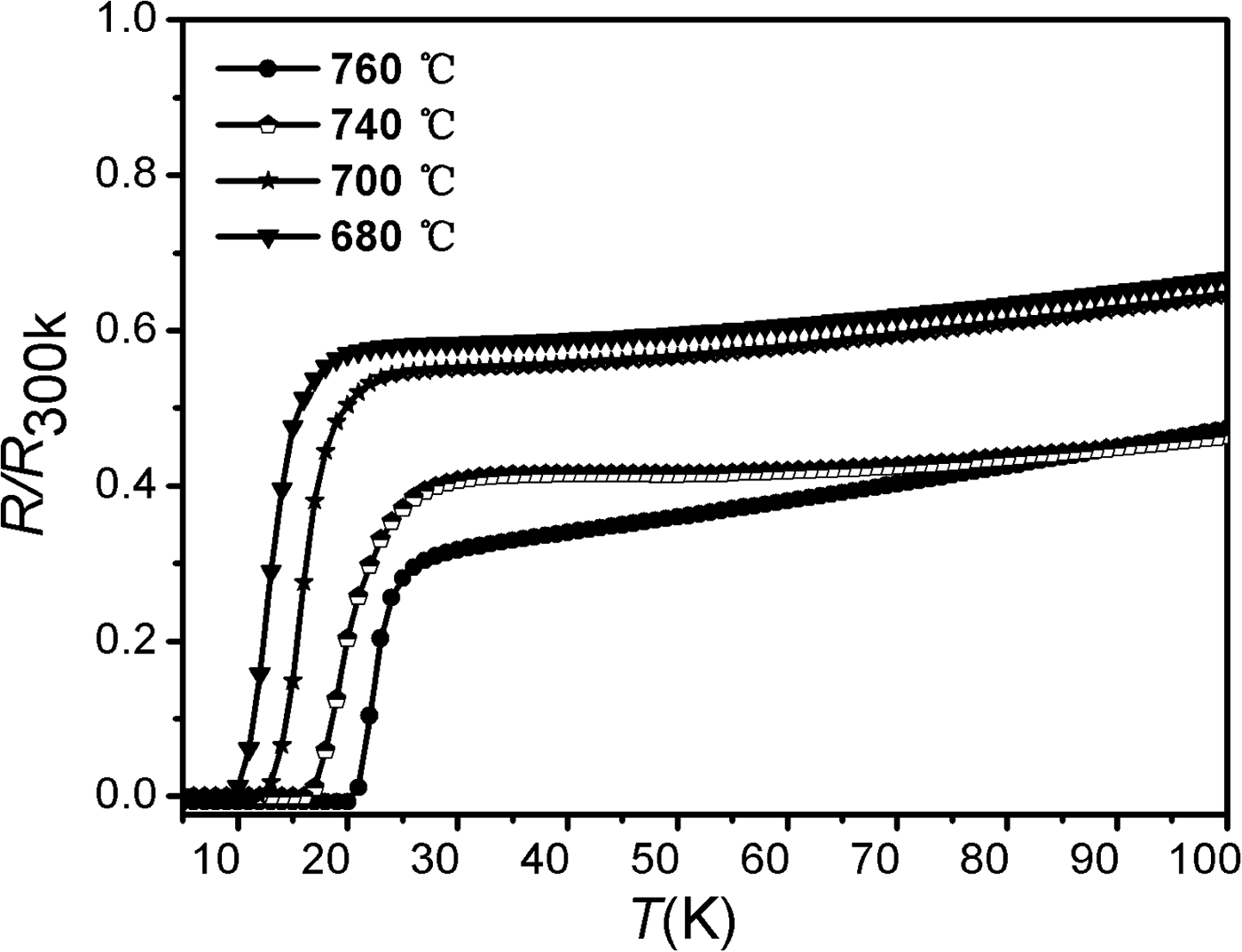
The XRD patterns for La1.8Sr0.2CuO4 films under different substrate temperatures are shown in Figure 3. The (002), (004), (060) and (008) diffraction peaks grow stronger with increasing temperature, whereas the peak intensities of the (103), (110), (200) crystal planes become weaker. The reason lies in the fact that the increase of temperature provides energy for deposited particles to migrate to the best possible positions that lead to the higher crystallinity and better quality of the films. This can also be observed from the increase of superconducting transition temperatures, see the right-hand side of Figure 4.
XRD patterns of La1.8Sr0.2CuO4 thin films deposited at different temperatures.
R–T curves of La1.8Sr0.2CuO4 thin films deposited at different temperatures.
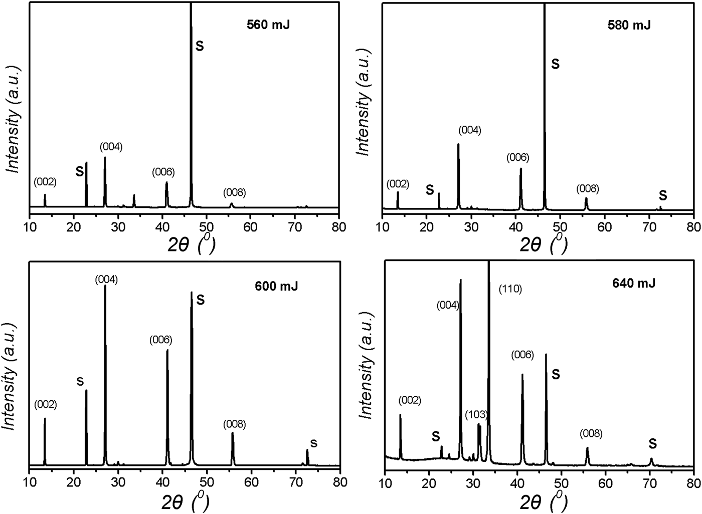
XRD patterns of La1.8Sr0.2CuO4 thin films deposited at different laser energies.
Laser energies of 560, 580, 600 and 640 mJ were selected in this work. Figure 5 presents the XRD patterns of the La1.8Sr0.2CuO4 thin film deposited at different laser energies. We can see that the peak intensity of the (00 l) aligned LSCO film at 600 mJ is higher than that at other laser energies.
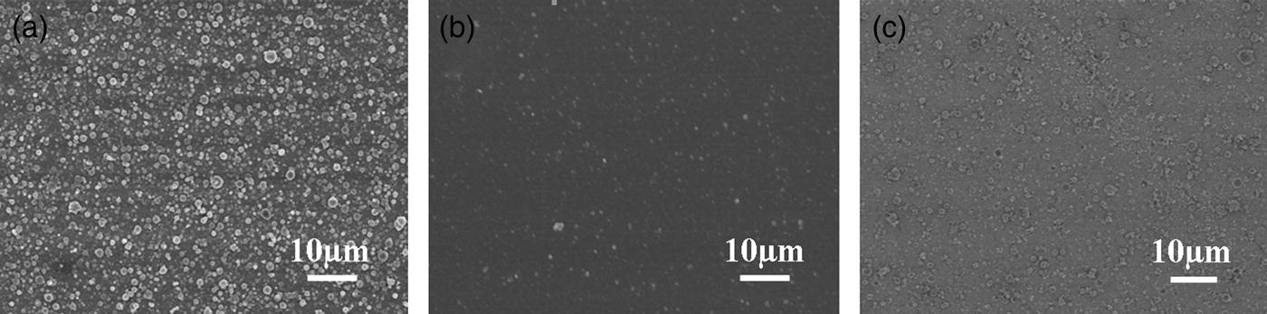
Figures 6(a)–6(c) show typical SEM images of La1.8Sr0.2CuO4 thin films deposited at different target–substrate distances. Large particles are observed clearly on the film surfaces in Figures 6(a) and 6(c), while the film surface in Figure 6(b) is smoother, which means that 4 cm target–substratedistance is more suitable for the growth of LSCO films.
SEM images of La1.8Sr0.2CuO4 thin films deposited at target–substrate distances: (a) 3.5 cm, (b) 4.0 cm, and (c) 4.5 cm.
The as-deposited thin film was in-situ annealed in oxygen ambient of 80 Pa at 580 °C for 30 min, and then gradually cooled to room temperature, aiming to supply the oxygen content for film.
I–V curves of the La1.8Sr0.2CuO4/La1.9Sr0.1CuO4 bilayers. The inset shows the layout of the bilayers.
C. Fabrication and characterization of bilayers
Each of the La1.8Sr0.2CuO4/La1.9Sr0.1CuO4 superconducting bilayers was prepared by PLD in the optimized parameters with which the monolayer was fabricated. Firstly, the bilayers sample was made to adhere to the inside of the Petri dish wall. By adding a dilute HNO3 solution in the Petri dish, three-quarters of the sample was flooded with the solution to ablate in 20 min. Then we took out the sample and used deionized water to wash the surface and dried it in time, so the film step of two different components was fabricated and then the I–V curves of the as-prepared bilayers were measured by the two-probe method.
We can see in Figure 7 that a fine rectifying property was observed at 5 K below the superconductor transition temperature which was better than that in the normal state. We consider that this may be related to the carrier mobility between the top and the bottom layers under the electric field.
IV. CONCLUSION
In summary, the targets of underdoped La1.8Sr0.2CuO4 and overdoped La1.9Sr0.1CuO4 were prepared by the conventional solid state reaction. The XRD analyses reveal that both the targets are single phase without detectable impurity. By exploring technological parameters for depositing La1.8Sr0.2CuO4 films by PLD, the optimal conditions were found to be 30 Pa oxygen pressure, 760 °C substrate temperature, 4 cm target–substrate distance, and 600 mJ laser energy. Using the optimized parameters, La1.8Sr0.2CuO4/La1.9Sr0.1CuO4 superconducting bilayers were successfully fabricated. By using the method of chemical corrosion, the film step of two different components was fabricated at the substrate surface, and then the I–V curves of the bilayers were measured, which show a fine rectifying property at 5 K below the superconductor transition temperature. This is possibly related to the tuning of carrier concentration and mobility in the different doped layers under the electric field.
ACKNOWLEDGMENTS
This work was supported by the National Basic Research Program of China (973 Program) (grant no. 2010CB933501), the National Natural Science Foundation of China (grant nos 51202218, 61274017, 61264007, and 61274009) and the Qianjiang Talent Program of Zhejiang Province (grant no. QJD1202004).