Introduction
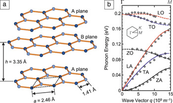
Graphene is a two-dimensional (2D) material, formed of a lattice of hexagonally arranged carbon atoms. The term graphene is typically applied to a single layer of graphite, although common references also exist to bilayer or trilayer graphene. (See the introductory article in this issue.) Most thermal properties of graphene are derived from those of graphite and bear the imprint of the highly anisotropic nature of this crystal.Reference Pierson1 For instance, the in-plane covalent sp 2 bonds between adjacent carbon atoms are among the strongest in nature (slightly stronger than the sp 3 bonds in diamond), with a bonding energyReference Schabel and Martins2 of approximately 5.9 eV. By contrast, the adjacent graphene planes within a graphite crystal are linked by weak van der Waals interactions2 (∼50 meV) with a spacingReference Bullett3 of h ≈ 3.35 Å. Figure 1a displays the typical ABAB (also known as Bernal) stacking of graphene sheets within a graphite crystal.
(a) Schematic of the atomic arrangement in graphene sheets. Dashed lines in the bottom sheet represent the outline of the unit cell. The areal density of carbon atoms in graphene is 3.82 × 1015 cm–2. (b) Graphene phonon dispersion along the Γ-to-M crystallographic direction.Reference Saito, Dresselhaus and Dresselhaus4–Reference Wirtz and Rubio7 Lines show numerical calculations; symbols represent experimental data. Note the presence of linear in-plane acoustic modes (longitudinal acoustic, LA; transverse acoustic, TA), as well as flexural out-of-plane acoustic (ZA) modes with a quadratic dispersion. The latter are responsible for many of the unusual thermal properties of graphene. Graphene has a much higher sound velocity and optical phonon (OP) energy than most materials; by comparison, OPs have energies of ∼0.035 eV in germanium and GaAs and ∼0.06 eV in silicon. LO, longitudinal optical; TO, transverse optical; ZO, out-of-plane optical.

The strong and anisotropic bonding and the low mass of the carbon atoms give graphene and related materials unique thermal properties. In this article, we survey these unusual properties and their relation to the character of the underlying lattice vibrations. We examine both the specific heat and thermal conductivity of graphene and related materials and the conditions for achieving ballistic, scattering-free heat flow. We also investigate the role of atomistic lattice modifications and defects in tuning the thermal properties of graphene. Finally, we explore the role of heat conduction in potential device applications and the possibility of architectures that allow control over the thermal anisotropy.
Phonon dispersion of graphene
To understand the thermal properties of graphene, one must first inspect the lattice vibrational modes (phonons) of the material. The graphene unit cell, marked by dashed lines in Figure 1a, contains N = 2 carbon atoms. This leads to the formation of three acoustic (A) and 3N – 3 = 3 optical (O) phonon modes, with the dispersionsReference Saito, Dresselhaus and Dresselhaus4–Reference Wirtz and Rubio7 shown in Figure 1b. The dispersion is the relationship between the phonon energy E or frequency ω (E = ħω, where ħ is the reduced Planck constant) and the phonon wave vector q. Longitudinal (L) modes correspond to atomic displacements along the wave propagation direction (compressive waves), whereas transverse (T) modes correspond to in-plane displacements perpendicular to the propagation direction (shear waves). In typical three-dimensional (3D) solids, transverse modes can have two equivalent polarizations, but the unique 2D nature of graphene allows out-of-plane atomic displacements, also known as flexural (Z) phonons.
At low q near the center of the Brillouin zone, the frequencies of the transverse acoustic (TA) and longitudinal acoustic (LA) modes have linear dispersionsReference Mingo and Broido8, Reference Nika, Pokatilov, Askerov and Balandin9 of ωTA ≈ v TAq and ωLA ≈ v LAq, respectively. The group velocities v TA ≈ 13.6 km/s and v LA ≈ 21.3 km/s are four to six times higher than those in silicon or germanium because of the strong in-plane sp 2 bonds of graphene and the small mass of carbon atoms.Reference Mingo and Broido8–Reference Muñoz, Lu and Yakobson11 In contrast, the flexural ZA modes have an approximately quadratic dispersion,Reference Mingo and Broido8, Reference Nika, Pokatilov, Askerov and Balandin9 ωZA ≈ αq 2, where α ≈ 6.2 × 10⁻⁷ m2/s. As we will discuss, the existence and modifications of these ZA modes are responsible for many of the unusual thermal properties of graphene.
Specific heat of graphene and graphite
The specific heat, C, of a material represents the change in energy density U when the temperature changes by 1 K, C = dU/dT, where T is the absolute temperature. The specific heat and heat capacity are sometimes used interchangeably, with units of joules per kelvin per unit mass, per unit volume, or per mole. The specific heat determines not only the thermal energy stored within a body but also how quickly the body cools or heats, that is, its thermal time constant τ ≈ RCV, where R is the thermal resistance for heat dissipation (the inverse of conductance, R = 1/G) and V is the volume of the body. Thermal time constants can be very short for nanoscale objects, on the order of 10 ns for nanoscale transistors,Reference Pop12 0.1 ns for a single graphene sheet or carbon nanotube (CNT),Reference Ong and Pop13 and 1 ps for the relaxation of individual phonon modes.Reference Ong, Pop and Shiomi14–Reference Qiu and Ruan16
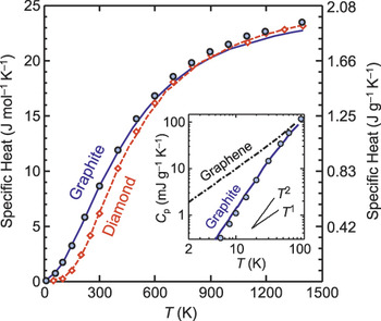
The specific heat of graphene has not been measured directly; thus, the short discussion here refers to experimental data available for graphite.Reference Tohei, Kuwabara, Oba and Tanaka17–Reference Nihira and Iwata19 The specific heat is stored by the lattice vibrations (phonons) and the free conduction electrons of a material, C = C p + C e. However, phonons dominate the specific heat of graphene at all practical temperaturesReference Nihira and Iwata19, Reference Benedict, Louie and Cohen20 (>1 K), and the phonon specific heat increases with temperature,Reference Tohei, Kuwabara, Oba and Tanaka17–Reference Benedict, Louie and Cohen20 as shown in Figure 2. At very high temperaturesReference Fried and Howard22 (approaching the in-plane Debye temperatureReference Tohei, Kuwabara, Oba and Tanaka17, Reference Tewary and Yang24 ΘD ≈ 2100 K), the specific heat is nearly constant at C p = 3N Ak B ≈ 25 J mol–1 K–1 ≈ 2.1 J g–1 K–1, also known as the Dulong–Petit limit. Here, N A is Avogadro’s number, and k B is the Boltzmann constant. This is the “classical” behavior of solids at high temperature when all six atomic degrees of motion (three translational and three vibrational) are excited and each carries 1/2k BT energy.
Specific heats of graphene, graphite, and diamond, all dominated by phonons at temperatures above ∼1 K. Lines show numerical calculations;Reference Popov10, Reference Tohei, Kuwabara, Oba and Tanaka17, Reference Hone21 symbols represent experimental data.Reference Nihira and Iwata19, Reference Fried and Howard22, Reference Reeber and Wang23 The inset indicates that the low-temperature specific heat of an isolated graphene sheet is expected to be higher than that of graphite because of the contribution of low-frequency ZA phonons (also see Figure 1b). Above ∼100 K, the specific heats of graphene and graphite should be identical. The inset makes use of different units to illustrate a common occurrence in practice (e.g., J mol–1 K–1, or J g–1 K–1, or J cm–3 K–1), but conversion is easily achieved by dividing and/or multiplying by the atomic mass of carbon (A = 12.01 g/mol) or the density of graphite (ρ ≈ 2.25 g/cm3).

At room temperature, the specific heat of graphite is C p ≈ 0.7 J g–1 K–1, approximately one-third of the classical upper limit.Reference Tohei, Kuwabara, Oba and Tanaka17, Reference Nihira and Iwata19 Interestingly, this value for graphite at room temperature is ∼30% higher than that of diamond because of the higher density of states at low phonon frequencies given by the weak coupling between graphite layers.Reference Tohei, Kuwabara, Oba and Tanaka17 A similar behavior is expected for an isolated graphene sheet at room temperature, when all of its flexural ZA modes should be thermally excited. However, it is possible that these modes could be partly suppressed or their dispersion altered when graphene is in strong contact with a substrate (thus lowering the specific heat), as suggested by experiments investigating epitaxial graphene on metalsReference Aizawa, Souda, Ishizawa, Hirano, Yamada, Tanaka and Oshima25, Reference Shikin, Farías and Rieder26 and recent theoretical work concerning graphene on insulators.Reference Ong and Pop27
At low temperatures (Figure 2 inset), the specific heat scales as C p ∼ Td/n for a phonon dispersion of ω ∼ qn in d dimensions.Reference Popov10, Reference Hone21 Thus, the low-temperature specific heat contains valuable information about both the dimensionality of a system and its phonon dispersion.Reference Hone21 The behavior of C p for an isolated graphene sheet should be linear in T at very low temperatures when the quadratic ZA modes dominate, followed by a transition to ∼T 2 behavior due to the linear LA and TA phononsReference Popov10, Reference Benedict, Louie and Cohen20, Reference Hone21 and eventually by a “flattening” to a constant as the high Debye temperature ΘD is approached, in the classical limit (Figure 2). Indeed, numerical calculations using the complete phonon dispersionReference Popov10, Reference Hone21 reveal that, for a wide temperature range (T < 50 K), C p is linear in T for isolated graphene, as shown in the Figure 2 inset. By contrast, the specific heat of graphite rises as ∼T 3 at very low temperature (<10 K) due to the weak interlayer coupling.Reference Nicklow, Wakabayashi and Smith18 In an intermediate temperature range (10–100 K), the C p value of graphite transitions to ∼T 2 behavior because of the in-plane linear phonons once the soft c-axis modes are fully occupied.Reference Benedict, Louie and Cohen20 This behavior is consistent with graphite having both 2D and 3D features and is shown in the Figure 2 inset. CalculationsReference Nihira and Iwata19 and recent measurementsReference Fong and Schwab28 have also estimated the specific heat of the electronic gas in graphene at low temperature, finding values on the order of C e ≈ 2.6 μJ g–1 K–1 at 5 K (three orders of magnitude lower than the phonon specific heat, C p, at this temperature). The value of C ein graphene is lower than those in other 2D electron gases, opening up interesting opportunities for graphene as a fast and sensitive bolometric detector.Reference Fong and Schwab28
Thermal conductivity of graphene: Intrinsic
The thermal conductivity (κ) of a material relates the heat flux per unit area, Q″ (e.g., in W/m2), to the temperature gradient, Q″ = –κ∇T. The sign in this relationship is negative, indicating that heat flows from high to low temperature. The thermal conductivity can be related to the specific heat by κ ≈ ∑Cvλ, where v and λ are the appropriately averaged phonon group velocity and mean free path, respectively.Reference Jeong, Datta and Lundstrom29 This expression is commonly used under diffusive transport conditions, when sample dimensions are much greater than the phonon mean free path (L ≫ λ). (We discuss the ballistic heat-flow regime in a later section.) For the purposes of heat transport, the “thickness” of a graphene monolayer is typically assumed to be the graphite interlayer spacing,Reference Bullett3h ≈ 3.35 Å.
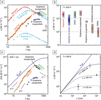
The in-plane thermal conductivity of graphene at room temperature is among the highest of any known material, about 2000–4000 W m–1 K–1 for freely suspended samplesReference Chen, Moore, Cai, Suk, An, Mishra, Amos, Magnuson, Kang, Shi and Ruoff30–Reference Chen, Wu, Mishra, Kang, Zhang, Cho, Cai, Balandin and Ruoff32 (Figure 3a–b). The upper end of this range is achieved for isotopically purified samples (0.01% 13C instead of 1.1% natural abundance) with large grains,Reference Chen, Wu, Mishra, Kang, Zhang, Cho, Cai, Balandin and Ruoff32 whereas the lower end corresponds to isotopically mixed samples or those with smaller grain sizes. Naturally, any additional disorder or even residue from sample fabricationReference Pettes, Jo, Yao and Shi42 will introduce more phonon scattering and lower these values further. For comparison, the thermal conductivity of natural diamond is ∼2200 W m–1 K–1 at room temperatureReference Anthony, Banholzer, Fleischer, Wei, Kuo, Thomas and Pryor39, Reference Berman43 (that of isotopically purified diamond is 50% higher, or ∼3300 W m–1 K–1), and those of other related materials are plotted in Figure 3a–b. In particular, Figure 3b shows presently known ranges of thermal conductivity at room temperature, with the implication that all lower bounds could be further reduced in more disordered samples.
(a) Thermal conductivity κ as a function of temperature: representative data for suspended graphene (open blue circles),Reference Chen, Wu, Mishra, Kang, Zhang, Cho, Cai, Balandin and Ruoff32 SiO2-supported graphene (solid blue squares),Reference Seol, Jo, Moore, Lindsay, Aitken, Pettes, Li, Yao, Huang, Broido, Mingo, Ruoff and Shi33 ∼20-nm-wide graphene nanoribbons (GNRs, solid magenta diamond),Reference Liao, Wu, Wang, Tahy, Jena, Dai and Pop34 suspended single-walled carbon nanotubes (SWCNTs, green crosses),Reference Pop, Mann, Wang, Goodson and Dai35 multiwalled CNTs (MWCNTs, solid orange circles),Reference Kim, Shi, Majumdar and McEuen36 type IIa diamond (open red diamonds),Reference Ho, Powell and Liley37 graphite in-plane (sideways open blue triangles),Reference Ho, Powell and Liley37 and graphite out-of-plane (upright open blue triangles).Reference Ho, Powell and Liley37 Additional data for graphene and related materials are summarized in Reference BalandinReferences 31 and Reference Sadeghi, Petters and Shi38. (b) Room-temperature ranges of thermal conductivity κ for diamond,Reference Anthony, Banholzer, Fleischer, Wei, Kuo, Thomas and Pryor39 graphite (in plane),Reference Balandin31 carbon nanotubes (CNTs),Reference Balandin31 suspended graphene,Reference Balandin31, Reference Chen, Wu, Mishra, Kang, Zhang, Cho, Cai, Balandin and Ruoff32 SiO2-supported graphene,Reference Seol, Jo, Moore, Lindsay, Aitken, Pettes, Li, Yao, Huang, Broido, Mingo, Ruoff and Shi33 SiO2-encased graphene,Reference Jang, Chen, Bao, Lau and Dames40 and GNRs.Reference Liao, Wu, Wang, Tahy, Jena, Dai and Pop34 (c) In-plane thermal conductance G per unit cross-sectional area A for graphene and related materials (symbols), compared to the theoretical ballistic limit, G ball/A (solid line).Reference Mingo and Broido8, Reference Muñoz, Lu and Yakobson11, Reference Saito, Nakamura and Natori41 (d) Expected scaling of thermal conductivity κ with sample length L in the quasiballistic regime at T ≈ 300 K. The solid line is the ballistic limit, κball = (G ball/A)L, and dashed lines represent κ estimated with phonon mean free paths as labeled (see text), chosen to match existing data for suspended graphene,Reference Chen, Wu, Mishra, Kang, Zhang, Cho, Cai, Balandin and Ruoff32 supported graphene,Reference Seol, Jo, Moore, Lindsay, Aitken, Pettes, Li, Yao, Huang, Broido, Mingo, Ruoff and Shi33 and GNRsReference Liao, Wu, Wang, Tahy, Jena, Dai and Pop34 from top to bottom, respectively; symbols are consistent with panels (a) and (c).

By contrast, heat flow in the cross-plane direction (along the c axis) of graphene and graphite is strongly limited by weak interplane van der Waals interactions. The thermal conductivity along the c axis of pyrolytic graphite is a mere ∼6 W m–1 K–1 at room temperature,Reference Pierson1, Reference Ho, Powell and Liley37 as shown in Figure 3a. Heat flow perpendicular to a graphene sheet is also limited by weak van der Waals interactions with adjacent substrates, such as SiO2. The relevant metric for heat flow across such interfaces is the thermal conductance per unit area, G″ = Q″/ΔT ≈ 50 MW m–2 K–1 at room temperature.Reference Chen, Jang, Bao, Lau and Dames44–Reference Mak, Lui and Heinz46 This is approximately equivalent to the thermal resistance of a ∼25-nm layer of SiO2Reference Pop12 and could become a limiting dissipation bottleneck in highly scaled graphene devices and interconnects,Reference Liao, Wu, Wang, Tahy, Jena, Dai and Pop34 as discussed in a later section. Interestingly, the thermal resistance, 1/G″, does not change significantly across few-layer graphene samplesReference Koh, Bae, Cahill and Pop45 (i.e., from one to 10 layers), indicating that the thermal resistance between graphene and its environment dominates that between individual graphene sheets. Indeed, the interlayer thermal conductance of bulk graphite is ∼18 GW m–2 K–1 if the typical spacing (Figure 1a) and c-axis thermal conductivity are assumed.
Thermal conductivity of graphene: Roles of edges and substrates
Despite its high room-temperature value for freely suspended samples, the in-plane thermal conductivity of graphene decreases significantly when this 2D material is in contact with a substrate or confined in graphene nanoribbons (GNRs). This behavior is not unexpected, given that phonon propagation in an atomically thin graphene sheet is likely to be very sensitive to surface or edge perturbations. At room temperature, the thermal conductivity of graphene supported by SiO2Reference Seol, Jo, Moore, Lindsay, Aitken, Pettes, Li, Yao, Huang, Broido, Mingo, Ruoff and Shi33 was measured as ∼600 W m–1 K–1, that of SiO2-encased grapheneReference Jang, Chen, Bao, Lau and Dames40 was measured as ∼160 W m–1 K–1, and that of supported GNRsReference Liao, Wu, Wang, Tahy, Jena, Dai and Pop34 was estimated as ∼80 W m–1 K–1 for ∼20-nm-wide samples. The broader ranges of presently known values at room temperature are summarized in Figure 3b. Although differences could exist between these studies in terms of defects introduced during sample fabrication, for example, the results nevertheless suggest a clear decrease in thermal conductivity from that of isolated (freely suspended) graphene, consistent with theoretical predictions.Reference Lindsay, Broido and Mingo47–Reference Aksamija and Knezevic49
For SiO2-supported graphene, the decrease in thermal conductivity occurs as a result of the coupling and scattering of graphene phonons with substrate vibrational modes,Reference Qiu and Ruan16 such that the graphene ZA branch appears to be most affected.Reference Ong and Pop27, Reference Seol, Jo, Moore, Lindsay, Aitken, Pettes, Li, Yao, Huang, Broido, Mingo, Ruoff and Shi33 This decrease is also seen in Figure 3c, expressed as thermal conductance per unit cross-sectional area (G/A), which is a more appropriate measure when samples approach ballistic heat-flow limits. For comparison, this figure also displays the thermal conductance of CNTsReference Pop, Mann, Wang, Goodson and Dai35, Reference Kim, Shi, Majumdar and McEuen36 and the theoretical upper limit of scattering-free ballistic transport (G ball/A) as calculated from the phonon dispersion.Reference Mingo and Broido8, Reference Muñoz, Lu and Yakobson11, Reference Saito, Nakamura and Natori41 (Also see the later section on ballistic transport.) Figure 3d illustrates the expected dependence of the room-temperature thermal conductivity on sample length L in a quasiballistic transport regime, as L becomes comparable to or smaller than the intrinsic phonon mean free path, λ0 ≈ 600 nm. When graphene is confined in GNRs that are narrower than the intrinsic phonon mean free path (width W ≤ λ0), phonon scattering with boundaries and edge roughness further reduces the thermal conductivityReference Haskins, Kınacı, Sevik, Sevinçli, Cuniberti and Çağın48, Reference Aksamija and Knezevic49 compared to the cases of suspended and SiO2-supported graphene.
It is relevant to put such thermal properties of graphene into context. For comparison, the thermal conductivity of thin Si-on-insulator (SOI) films is also strongly reduced from the bulk silicon value (∼150 W m–1 K–1 at room temperature) to ∼25 W m–1 K–1 in ∼20-nm thin films as a result of surface scattering.Reference Liu and Asheghi50 This value is further reduced to ∼2 W m–1 K–1 in ∼20-nm-diameter silicon nanowires with rough surfaces.Reference Chen, Hochbaum, Murphy, Moore, Yang and Majumdar51 At comparable linewidths, the thermal conductivity of copper interconnects is on the order of ∼100 W m–1 K–1 (a factor of four lower than that of bulk copper) based on the Wiedemann–Franz law that relates the thermal and electrical conductivity of metals.Reference Steinhögl, Schindler, Steinlesberger, Traving and Engelhardt52 In contrast, despite substrate or edge effects, graphene maintains a relatively high thermal conductivity in 2D monolayer films that are atomically thin (h ≈ 3.35 Å), a size regime where no 3D materials can effectively conduct heat.
Thermal modeling of graphene
Given that thermal measurements of graphene are challenging because of its atomic thinness, modeling and simulation have played a key role in developing an understanding of graphene properties.Reference Klemens and Pedraza53 Existing methods for modeling thermal transport in graphene and GNRs include atomistic techniques such as molecular dynamics (MD),Reference Qiu and Ruan16, Reference Ong and Pop27, Reference Hu, Ruan and Chen54–Reference Zhong, Huang, Deng and Ai60 nonequilibrium Green’s functions (NEGF),Reference Xu, Chen, Wang, Gu and Duan61–Reference Yang, Ni, Jiang and Li64 and Boltzmann transport equation simulations.Reference Nika, Pokatilov, Askerov and Balandin9, Reference Seol, Jo, Moore, Lindsay, Aitken, Pettes, Li, Yao, Huang, Broido, Mingo, Ruoff and Shi33, Reference Lindsay, Broido and Mingo47, Reference Aksamija and Knezevic49 The following discussion focuses on MD simulations, which have provided atomistic insights into graphene heat flow and have also predicted novel routes for tailoring the thermal properties of nanostructured graphene materials.
Insights from molecular dynamics
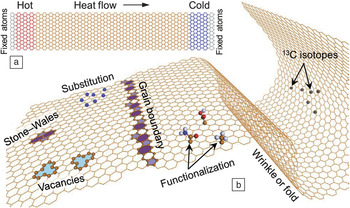
MD is a deterministic approach for investigating properties of molecular systems that employs empirical interactions between atoms as a “force field” and follows classical Newtonian dynamics.Reference Frenkel and Smit65Figure 4a schematically illustrates one of the two nonequilibrium molecular dynamics (NEMD) methodologies that are routinely used to investigate thermal transport in graphene or GNRs. In this methodology, atoms at both ends are kept fixed while near-end portions of a few nanometers are treated as hot and cold regions. By imposing either constant-heat-flux or constant-temperature boundary conditions in the hot and cold regions, a steady-state temperature gradient is introduced within the graphene sheet, which is then used to estimate the material thermal conductivity.
(a) Schematic of nonequilibrium molecular dynamics (NEMD) methodology for examining thermal transport in a GNR. (b) GNR showing different types of defects (vacancies, grain boundaries, Stone–Wales defects, substitutional and functionalization defects, and wrinkles or folds) that have a profound effect on tuning thermal transport in graphene. Also see Table I.

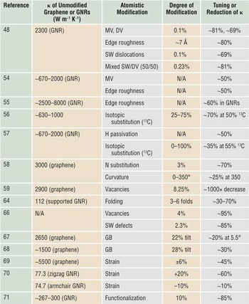
MD simulations have revealed how heat flow can be tuned or altered with respect to that of pristine graphene by introducing atomistic alterations of the honeycomb lattice. Such alterations are achieved through vacancies or Stone–Wales defects,Reference Haskins, Kınacı, Sevik, Sevinçli, Cuniberti and Çağın48, Reference Zhang, Lee and Cho59, Reference Hao, Fang and Xu66 grain boundaries,Reference Bagri, Kim, Ruoff and Shenoy67, Reference Cao and Qu68 strain,Reference Li, Maute, Dunn and Yang69, Reference Wei, Xu, Wang and Zheng70 chemical functionalization,Reference Chien, Yang and Chen71 isotopic impurities (13C)Reference Zhang, Lee, Fonseca, Borders and Cho56, Reference Hu, Schiffli, Vallabhaneni, Ruan and Chen57 or substitutional defects,Reference Mortazavi, Rajabpour, Ahzi, Remond and Allaei58 and edge roughnessReference Hu, Ruan and Chen54, Reference Evans, Hu and Keblinski55, Reference Hu, Schiffli, Vallabhaneni, Ruan and Chen57 or foldingReference Yang, Ni, Jiang and Li64 in GNRs, as shown in Figure 4b. Alterations or defects can reduce the thermal conductivity of graphene by an order of magnitude or more below its intrinsic value, as summarized in Table I. Such a reduction in thermal conduction could be interesting for thermoelectric applications, if the high electronic conduction of graphene can be preserved.Reference Sevinçli and Cuniberti72
Summary of simulation results for tuning or reduction in thermal conductivity of graphene through various atomistic modifications (also see Figure 4)

N/A, not available.
DV, diatomic vacancies; GB, grain boundary; MV, monatomic vacancies; SW, Stone–Wales.
Another interesting feature predicted by thermal MD simulations of graphene is that of thermal rectification. By analogy with electrical rectification in a p–n diode, a thermal rectifier would allow greater heat flux in one direction than another, that is, Q BA > Q AB for the same temperature difference ΔT BA = ΔT AB between its two terminals A and B.Reference Pop12 Any type of spatial variability that introduces asymmetry in the phonon density of states of the hot and cold regions has been suggested as a key criterion necessary for thermal rectification. For graphene, such a feature has been identified by MD simulations by introducing either shape asymmetry within the nanostructure (such as a thickness-modulated GNR,Reference Zhong, Huang, Deng and Ai60 tapered-width GNR,Reference Hu, Ruan and Chen54, Reference Yang, Zhang and Li73 or Y-shaped GNRReference Zhang and Zhang74) or mass asymmetry through substitution with 13C isotopes.Reference Pei, Zhang, Sha and Shenoy75 In addition, a recent study has also suggested that asymmetry in thermal reservoirs is as essential as system asymmetry in achieving thermal rectification in any system.Reference Lee, Varshney, Roy, Ferguson and Farmer76 No matter how it is achieved, the modulation of directional heat flux could provide novel functionality in future nanoelectronic devices such as thermal rectifiers, thermal transistors, and thermal logic gates.
Nevertheless, the results of MD simulations should be interpreted in the proper context.Reference Sadeghi, Petters and Shi38 The main strength of the MD approach is that it can be used to analyze the effects of atomistic changes on the thermal properties of a nanomaterial (Figure 4 and Table I). However, MD is a semiclassical technique that overestimates the specific heat below the Debye temperature, ΘD. Graphene has a very high Debye temperature, ΘD ≈ 2100 K, such that the specific heat at room temperature is only about one-third that of the classical Dulong–Petit limit (Figure 2). MD results are also sensitive to the choice of interatomic potential.Reference Zhang, Lee and Cho59, Reference Lindsay and Broido77 Thus, absolute values of thermal conductivity for graphene and GNRs calculated by MD span a wide range (75–10,000 W m–1 K–1; see Table I) because of differences in interatomic potentials,Reference Zhang, Lee and Cho59, Reference Lindsay and Broido77 boundary conditions, and simulated system dimensions (often 10 nm or smaller). The effect of system dimensions is more challenging in graphene than in other materials because of the very large intrinsic phonon mean free path, λ0 ≈ 600 nm (see the next section). Thus, MD simulations should generally be interpreted based on the relative changes rather than the absolute values of the thermal properties they predict. Such changes are listed in the last column of Table I.
Ballistic limit of graphene thermal conductivity
Whereas the classical regime of large sample size (L ≫ λ0) suggests a constant thermal conductivity, κ, and a thermal conductance that scales inversely with length, G = κA/L, quantum treatment of small graphene devices (L ≪ λ0) reveals that the thermal conductance approaches a constant (G ball), independent of length,Reference Mingo and Broido8, Reference Muñoz, Lu and Yakobson11, Reference Saito, Nakamura and Natori41 in ballistic, scattering-free transport. Thus, the relationship between conductivity and conductance imposes that the effective thermal conductivity of a ballistic sample must be proportional to its length as κball = (G ball/A)L, where A is the cross-sectional area, A = Wh. This is an important distinction also made between the electrical conductance, which reaches a constant value (e.g., ∼155 μS in single-walled CNTs with four quantum channelsReference Javey, Guo, Paulsson, Wang, Mann, Lundstrom and Dai78, Reference Park, Rosenblatt, Yaish, Sazonova, Üstünel, Braig, Arias, Brouwer and McEuen79), and the electrical conductivity and mobility, which appear to depend on the device length in the ballistic regime.Reference Shur80, Reference Wang and Lundstrom81
The ballistic thermal conductance of graphene can be numerically calculatedReference Mingo and Broido8, Reference Muñoz, Lu and Yakobson11, Reference Saito, Nakamura and Natori41 from the phonon dispersion (Figure 1b) and is shown by the solid line in Figure 3c. This upper ballistic limit can also be approximated analyticallyReference Mingo and Broido8 as G ball/A ≈ 6 × 10⁵T 1.5 W m–2 K–5/2 for T < 100 K. The ∼T 1.5 dependence arises from the dominance of flexural ZA modes at low temperatures, with a specific heat C ∼ T and a phonon dispersion with ω ∼ q 2. A comparison with the currently available experimental data in terms of conductance per unit area (symbols in Figure 3c) reveals that various measurements have reached only a fraction of this ballistic limit. For instance, 10-μm-long graphene supported on SiO2Reference Seol, Jo, Moore, Lindsay, Aitken, Pettes, Li, Yao, Huang, Broido, Mingo, Ruoff and Shi33 reached ∼2%, and 2.8-μm long suspended graphene samplesReference Chen, Wu, Mishra, Kang, Zhang, Cho, Cai, Balandin and Ruoff32 reached ∼25% of the theoretical ballistic thermal conductance limit at room temperature.
The transition of thermal conductivity from the ballistic (L ≪ λ0) to the diffusive (L ≫ λ0) heat-flow regime can be approximated through a Landauer-like approachReference Jeong, Datta and Lundstrom29, Reference Prasher82 as κ(L) ≈ G ball/A[1/L + 2/(πλ)]–1, where the factor of π/2 accounts for angle averagingReference Jeong, Kim, Luisier, Datta and Lundstrom83 in two dimensions to obtain the backscattering length responsible for the thermal resistance. Fitting this simple expression to the experimental data in Figure 3d reveals phonon mean free paths at room temperature of λ0 ≈ 600 nm in suspended graphene (also referred to here as the intrinsic mean free path), λ ≈ 100 nm in graphene supported on SiO2, and λ ≈ 20 nm in GNRs (of width ∼20 nm) supported on SiO2. These are some of the key length scales needed for understanding graphene thermal properties in nanometer-size devices. The ballistic upper limit of thermal conductivity in a graphene sample of length L ≈ 100 nm can now be estimated as κball ≈ 350 W m–1 K–1 at room temperature. We note that suspended graphene should attain >80% of the ballistic heat-flow limit in samples shorter than L < 235 nm, whereas graphene supported on SiO2 reaches this level at L < 40 nm, well within the means of modern nanofabrication.
Thermal properties for applications
Devices and interconnects
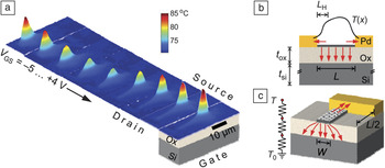
In the context of nanoscale devices and interconnects, graphene is often thought to hold advantages over other materials because of its higher thermal conductivity. Thus, high thermal conductivity could suggest very good heat sinking and low temperature rise during device operation. However, under high-field and high-temperature (i.e., typical circuit) operating conditions, significant dissipation and temperature rise can nevertheless occur in graphene devices,Reference Liao, Wu, Wang, Tahy, Jena, Dai and Pop34, Reference Bae, Islam, Dorgan and Pop84 as shown in Figure 5.
(a) Infrared (IR) imaging of temperature in a functioning graphene field-effect transistor (GFET) with a drain bias of V DS = –12 V and varying gate bias.Reference Bae, Islam, Dorgan and Pop84 The device is back-gated, allowing IR imaging from the top. The hot spot marks the location of lowest carrier density (which changes with voltage bias) and highest electric field. (b) Longitudinal cross section of a graphene device or interconnect, showing heat dissipation pathways (red arrows) and temperature profile T(x). The device, of length L and width W, is supported by an insulator (e.g., SiO2) of thickness t ox on a silicon substrate of thickness t Si. The bottom of the substrate and the palladium contacts are assumed to be at temperature T 0. Significant heat can flow to the contacts only within a distance of the thermal healing length L H, reducing the temperature of devices shorter than ∼3L H, or ∼0.3 μm. (c) Transverse cross section showing heat dissipation from a narrow GNR (W < t ox), which benefits from lateral heat spreading into the substrate and can carry peak current densities (∼109 A/cm2) higher than those carried by wide graphene ribbons.Reference Liao, Wu, Wang, Tahy, Jena, Dai and Pop34, Reference Behnam, Lyons, Bae, Chow, Islam, Neumann and Pop85

Self-heating of graphene devices and interconnects at high field begins through the emission of optical phonons (OPs),Reference Barreiro, Lazzeri, Moser, Mauri and Bachtold86–Reference Perebeinos and Avouris88 similarly to the case of CNTs. OPs are strongly emitted at applied voltages comparable to or greater than their energy (∼0.16 eV; see Figure 1b), although smaller biases can also be sufficient because of the long Fermi tail of the electron (or hole) distribution. OPs decay on time scales of ∼1 ps into lower-energy acoustic phonons (APs).Reference Ong, Pop and Shiomi14, Reference Kang, Abdula, Cahill and Shim89 However, given their comparatively large specific heat, the AP temperature lags behind that of the electrons and OPs by ∼1–10 ns after a voltage pulse is applied. (This delay also depends on the thermal resistance between the device and the surrounding environment.Reference Pop12)
The pathway of heat dissipation to the environment heat sink becomes key in determining the temperature rise once steady state is reached and thus, ultimately, the reliability of graphene devices. In other words, despite (or perhaps because of) the excellent intrinsic thermal properties of graphene, dissipation from graphene devices is often limited by their interfaces, contacts, and surrounding materials, which are often thermal insulators such as SiO2. To illustrate this point, Figure 5a shows temperature profiles recorded by infrared thermal imagingReference Bae, Islam, Dorgan and Pop84 along a graphene device on SiO2 under a constant drain–source bias (V DS = –12 V) as the gate voltage (V GS) is varied from –5 V to 4 V. The complex temperature profile occurs because the carrier density and, thus, the electric field are not constant along the device at high bias. Consequently, the temperature hot spot marks the location of maximum electric field and minimum carrier concentration.Reference Bae, Islam, Dorgan and Pop84
A schematic of dissipation in a graphene device is shown in Figure 5b, where heat flow can occur either into the substrate or to the metal contacts.Reference Liao, Wu, Wang, Tahy, Jena, Dai and Pop34, Reference Grosse, Bae, Lian, Pop and King90 The length scale for lateral heat flow to the contacts is the thermal healing length L H ≈ (κWh/g)1/2, where W is the device width, g is the thermal conductance to the substrate per unit length,Reference Liao, Wu, Wang, Tahy, Jena, Dai and Pop34 and other symbols are as previously defined. The total thermal conductance g includes the contribution from the graphene–substrate interface and that from any underlying layers (e.g., SiO2 and Si in Figure 5b). For typical supporting oxide thicknesses (t ox ≈ 90–300 nm) and interfacial thermal conductances G″, L H≈ 0.1–0.2 μm.
Numerical calculations suggest that only devices shorter than ∼3L H ≈ 0.3–0.6 μm benefit from substantial cooling through the metal contacts.Reference Liao, Wu, Wang, Tahy, Jena, Dai and Pop34, Reference Behnam, Lyons, Bae, Chow, Islam, Neumann and Pop85 For long devices (L ≫ 3L H), the dissipation occurs almost entirely through the graphene–substrate interface (of thermal resistance 1/G″) and through the underlying substrate (e.g., SiO2/Si, BN/Si, SiC). For narrow devices (W < t ox) such as GNRs, a substantial amount of lateral heat spreading into the underlying oxide can also play a role,Reference Liao, Wu, Wang, Tahy, Jena, Dai and Pop34 as illustrated in Figure 5c. Finally, for devices that are both long and wide (L, W ≫ L H, t ox), the total thermal resistance can be estimated simply asReference Dorgan, Bae and Pop87R th ≈ 1/(G″A) + t ox/(κoxA) + 1/(2κSiA 1/2), where κox and κSi are the thermal conductivities of SiO2 and silicon, respectively; A = LW is the device area; and other variables are as defined in Figure 5. The final term approximates the spreading thermal resistance in the silicon substrate, which is assumed to be much thicker than both t ox and the graphene device dimensions. We note that improved heat sinking can be obtained by placing devices on substrates with a thinner supporting insulatorReference Behnam, Lyons, Bae, Chow, Islam, Neumann and Pop85 or higher thermal conductivity, as long as the graphene–substrate interface is not the limiting factor.Reference Chen, Jang, Bao, Lau and Dames44–Reference Mak, Lui and Heinz46
Recent work has also suggested that graphene devices might benefit from thermoelectric (Peltier) cooling at the metal contacts,Reference Grosse, Bae, Lian, Pop and King90 where a substantial difference in Seebeck coefficient exists. However, it is important to realize that, because of the one-dimensional nature of current flow, Peltier effects of opposite sign will occur at the two contacts, such that one cools as the other heats. Thus, additional contact engineering must be done to adjust the overall device temperature, for example, using asymmetric contacts, from the point of view of either geometry (one larger contact to sink heat) or materials (two contacts with different Seebeck coefficients).
3D architectures
As summarized earlier, because of its 2D nature, graphene has very high anisotropy of its thermal properties between the in-plane and out-of-plane directions. Whereas the in-plane thermal conductivity is excellent (>1000 W m–1 K–1), the out-of-plane thermal coupling is limited by weak van der Waals interactions and could become a thermal dissipation bottleneck. To overcome this effect in practice, 3D architectures could incorporate CNT–pillared graphene network (PGN) structures,Reference Dimitrakakis, Tylianakis and Froudakis91 interconnected CNT truss-like structures,Reference Tylianakis, Dimitrakakis, Melchor, Dobado and Froudakis92 and networked graphene flakes.Reference Chen, Ren, Gao, Liu, Pei and Cheng93 These 3D architectures (Figure 6) are envisioned as a new generation of nanomaterials with tunable thermomechanical functionality, leveraging the best aspects of both graphene and CNTs. Such structures could have numerous applications, enabling efficient electrodes for fuel cells,Reference Zhang, Sherrell, Minett, Razal and Chen94 nanoporous structures with very high surface area for hydrogen storage,Reference Dimitrakakis, Tylianakis and Froudakis91 supercapacitors,Reference Du, Yu, Dai, Ganguli, Varshney and Roy95 and tailored multidimensional thermal transport materials.
Schematic of a three-dimensional nanoarchitecture that combines carbon nanotube pillars and graphene sheets to achieve tunable cross-plane thermal transport. For instance, reducing the interjunction distance (IJD) and increasing the interlayer distance (ILD) could mitigate the weak interlayer thermal coupling of a graphene stack for higher cross-plane thermal conductivity. Conversely, longer IJD and shorter ILD could lower the cross-plane thermal conductivity, leading to thermal insulator or thermoelectric applications.

From the perspective of thermal transport, recent modeling studies suggest that the lateral CNT separation, called the interjunction distance (IJD), and the interlayer distance (ILD) between graphene sheets play a critical role in determining the thermal transport properties in these 3D architectures.Reference Varshney, Patnaik, Roy, Froudakis and Farmer96, Reference Varshney, Roy, Froudakis and Farmer97 When the lateral CNT separation, IJD, is on the order of tens of nanometers, the ballistic nature of heat propagation (because of the large phonon mean free path in graphene and CNTs) causes phonon scattering to occur primarily at the CNT/graphene junction nodes. These junctions, in turn, will govern the thermal conductivity of such architectures. Furthermore, because the carbon atoms and sp 2bonds of CNTs and graphene are the same, the phonon spectra are similar, and the junctions have very low interface thermal resistance. Hence, the thermal transport in different directions could be manipulated by tailoring the IJDs and ILDs.
For instance, the predicted interface thermal conductance at a junctionReference Bagri, Kim, Ruoff and Shenoy67, Reference Cao and Qu68 (∼10 GW m–2 K–1) is comparable to that between graphite layers (∼18 GW m–2 K−1) and over two orders of magnitude higher than the graphene thermal coupling with a substrate (∼50 MW m–2 K–1 at room temperatureReference Chen, Jang, Bao, Lau and Dames44–Reference Mak, Lui and Heinz46). This suggests that very dense packing of long CNTs (i.e., small IJD, large ILD) could significantly increase the out-of-plane thermal conductivity of the PGN architecture, by reducing the number of interfaces and “replacing” them with CNTs.Reference Du, Yu, Dai, Ganguli, Varshney and Roy95 On the other extreme, using short but widely spaced CNTs in the PGN structure would substantially reduce thermal conduction in the out-of-plane directionReference Du, Yu, Dai, Ganguli, Varshney and Roy95 (because of the small ILD, higher interface density, and low CNT areal density), thus possibly opening several routes for thermoelectric applications where extremely low thermal conductivity is desired. Over the past few years, multiple research groups have successfully synthesized CNT pillared-graphene architectures, and different property characterizations are underway.Reference Du, Yu, Dai, Ganguli, Varshney and Roy95, Reference Paul, Ghazinejad, Penchev, Lin, Ozkan and Ozkan98–Reference Yu, Lu, Bo, Mao and Chen100
Summary
The unusual thermal properties of graphene include very high in-plane thermal conductivity (strongly affected by interfacial interactions, atomic defects, and edges) and relatively low out-of-plane thermal conductance. The specific heat of graphene is dominated by phonons and is slightly higher than that of graphite and diamond below room temperature. The in-plane thermal conductance G of graphene can reach a significant fraction of the theoretical ballistic limit in submicrometer samples, owing to the large phonon mean free path (λ ≈ 100 to 600 nm in supported and suspended samples, respectively). Nevertheless, this behavior leads to an apparent dependence of thermal conductivity κ on sample length, similar to the behavior of mobility in quasiballistic electronic devices.
In the context of integrated electronics, heat dissipation from graphene devices and interconnects is primarily limited by their environment and the relatively weak van der Waals interfaces of graphene. In the context of graphene composites and 3D architectures, simulation results have suggested that the thermal properties could be highly tunable. Such tunability raises the interesting prospects of both ultrahigh thermal conductivity for heat-sinking applications and ultralow thermal conductivity for thermoelectric applications.
Acknowledgments
E.P. acknowledges assistance from Zuanyi Li, Andrey Serov, Pierre Martin, Ning Wang, Albert Liao, Changwook Jeong, and Mark Lundstrom, as well as funding from the AFOSR Young Investigator Program (YIP) award, the ARO Presidential Early Career (PECASE) award, and the Nanotechnology Research Initiative (NRI). V.V. and A.K.R. acknowledge Dr. Byung-Lip (Les) Lee (AFOSR Task 2302BR7P) and Dr. Joycelyn Harrison (AFOSR Task 2306CR9P) for funding from AFOSR.