Experimental evidence suggests that grain boundary-mediated deformation mechanisms dominate when the grain size is below a certain critical size (40–100 nm, depending upon the material).[Reference Wang, Wang, Aust and Erb1–Reference Gianola, Van Petegem, Legros, Brandstetter, Van Swygenhoven and Hemker5] Grain boundary-mediated mechanisms may include grain rotation, grain boundary migration, and grain boundary sliding. The transition from dislocation-based plasticity to grain boundary-mediated processes changes the overall deformation response. Nanoscale thin films showing minimum amount of ductility and failure are found to be due to brittle crack propagation.[Reference Haque and Saif6, Reference Haque and Saif7] Transition from dislocation plasticity to grain boundary-mediated process may lead to flaw insensitive behavior as reported in recent studies on aluminum thin films for both static and dynamic loading.[Reference Kumar, Haque and Gao8–Reference Kumar, Li, Haque and Gao10] At the grain size range of 50–60 nm, grain rotation is found to be the active deformation mechanism. These studies relate the effect of stress concentration on material deformation. This behavior is very important for the failure characteristics and reliability of nanoscale thin films. However, different materials have different critical grain size[Reference Wang, Wang, Aust and Erb1] for transition and deformation behavior may be determined by the competing mechanisms as mentioned above. Recently, it has been shown that platinum (Pt) thin films exhibit grain growth as a mechanism to relax externally applied mechanical stress.[Reference Sharon, Su, Prinz and Hemker11–Reference Gao, Rudneva, McGarrity, Xu, Prins, Thijssen, Zandbergen and Zant13] In this study, we take an experimental approach to understand the mechanics behind stress-induced grain growth and its effect on resulting deformation behavior. We used a nanofabricated uniaxial tension/fracture setup inside a transmission electron microscope (TEM) to obtain quantitative information on stress and strain, while directly visualizing the qualitative deformation (such as grain growth, rotation, and dislocation motion) characterization.
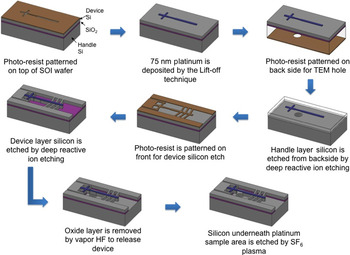
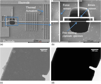
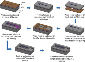
We developed a unique mechanical testing setup for single edge notched freestanding thin films using nanofabrication techniques. The device structure includes a set of electro-thermal actuators[Reference Kumar, Haque and Gao8, Reference Zhu and Espinosa14] to apply uniaxial tensile stress on a free-standing platinum specimen as well as force and strain sensors.[Reference Kumar, Haque and Gao8–Reference Kumar, Li, Haque and Gao10, Reference Haque and Saif15] Thermal actuators can possibly heat the specimen. We minimized the heat conduction toward the specimen using the heat sink beams[Reference Zhu, Corigliano and Espinosa16] as well as maximizing the distance between the specimen and the actuator beams.[Reference Kumar, Wolfe and Haque17] It has been reported that the distance between the actuator and the specimen does not affect the temperature rise at the specimen end. However, the device designed with heat sink beams is found to effectively keep the temperature rise at specimen end to minimum.[Reference Kumar, Wolfe and Haque17] The freestanding specimen is co-fabricated with these actuators, which eliminates conventional challenges in specimen gripping and alignment. The device fabrication process is explained in Fig. 1. The fabricated device, as shown in Figs. 2(a) and 2(b), is then placed on a chip carrier and attached to a custom-made TEM specimen holder with electrical feed through. While the samples are microfabricated, the notches are milled using Focused Ion Beam (FIB) at 10 pA of ion beam current. The ion beam might induce grain growth at the notch tip when higher currents are used. We found that for an ion beam current of 10 pA damage was non-existent (supplementary material). A JEOL 2010 LaB6 TEM operating at 200 kV of accelerating voltage was used for the experiments in this study.
Schematic showing different process steps for nanofabrication of a chip containing freestanding specimen and micro-actuators. The overall size of the chip allows in-situ TEM experiments.
Scanning electron microscope micrograph showing (a) fabricated device, (b) freestanding Pt specimen, TEM micrograph showing (c) specimen 1 and (d) specimen 2.
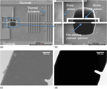
Platinum thin films, when deposited by e-beam evaporation, have a very small average grain size (~5–8 nm). At this average grain size and with a thickness of 75 nm, platinum becomes difficult to image in TEM [Figs. 2(c) and 2(d)]. Moreover, a large number of deformation processes will not be observable (even if active) at this grain size. In order to clearly understand and observe active deformation mechanisms we needed larger average grain size. We utilized AC voltage-based resistive heating to anneal the specimen and grow the grains to the required size. We performed such an annealing process on the specimen in situ inside the TEM, thus allowing us to observe and control the grain growth. In this work, we stopped the annealing process when most of the grains were approximately 10 nm or more.
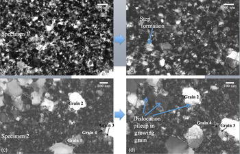
In a typical experiment, the notched section is observed under the TEM as the stress is slowly applied by supplying current through thermal actuator beams. For each step (0.1 V) increase in applied voltage, bright field images are recorded for the deformation mechanism at the notch tip. Then selected area electron diffraction pattern at and away from the notched section was recorded while also recording the motion of stress and strain sensor. During our first experiment, incremental increase in strain did not show any significant change at or away from the notch tip. At the stress of approximately 380 MPa, we found the evidence of grain growth at the notch tip as shown in Fig. 3(b). In another set of experiments we not only observed the grain growth at the notch tip but also observed significant grain growth slightly away from the notch tip as shown in Figs. 3(c) and 3(d).
TEM micrographs recorded at the notch tip for specimen 1-(a) 0.14% strain and 290 MPa, (b) 380 MPa and 0.25% strain; TEM micrograph at the notch tip for specimen 2- (c) zero strain, (d) 0.25% strain.
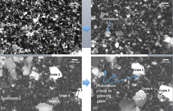
We did not calculate the change in area of grains in the first experiment because it is difficult to identify the starting grain. For the second experiment, we calculated the change in area of grains due to size change. We found that the grain marked as Grain 1 has changed from 14115 to 43801 nm2. Similarly, change in area for the grain marked as grain 2 is from 28278 to 32929 nm2. Grain 1 showed very large grain growth. This grain was closer to the notch tip as compared to Grain 2. Also, this grain does not lie on the notched section whereas Grain 2 does. We carefully observed the grain structure at the notch tip too. Grain 3 and Grain 4 show significant grain growth. Grain 3 went from 1621 nm2 to 4107 nm2. We have further marked the boundaries of some grains to the left of Grain 2 where significant grain growth is observed. Figure 3 clearly shows extensive growth at and away from the notch tip under tensile loading.
In the absence of any thermal activation we believe that grain growth is stress activated. In order to confirm our assertion, we need quantitative information regarding the grain growth process. In our first experiment, we did not observe grain growth at the notch tip for a strain of 0.14% and 290 MPa of stress as shown in Fig. 3(a). We started to see incremental grain growth as stress is increased beyond 290 MPa and for 0.25% strain and 380 MPa of stress large grain growth at the notch tip as well as away from it is observed as shown in Fig. 3(b). The critical stress for grain growth is calculated to be 290 MPa. We propose that the spontaneous grain growth can be attributed to be a mechanism to alleviate the stress concentration at the notch tip. For a notch tip radius of 65 nm and a notch depth of 300 nm, we calculated the stress concentration factor (theoretical) of ~5.3[Reference Baratta and Neal18] and will result in a notch tip stress of ~1.5 GPa. The theory by Gutkin and Ovid'ko[Reference Gutkin and Ovid'ko19] predicts the minimum external shear stress causing stable interface motion and an estimate of the larger shear stress leading to unstable grain boundary motion. The minimum external shear stress to cause stable interface motion is given by
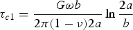 $$\tau _{c1}=\displaystyle{{G\omega b} \over {2\pi \lpar 1 - \nu \rpar 2a}}\ln \displaystyle{{2a} \over b}$$
where G denotes the shear modulus, ν the Poisson's ratio, b the interatomic distance, 2a the grain size and ω the tilt misorientation between grains. To approximate the minimum shear stress in the current case we assume G = 61 GPa, ν = 0.38, ω = 5° and 30°, b = 0.25 nm, and 2a = 15 and 50 nm. We calculate the minimum shear stress required for stable grain boundary migration τc1=39 MPa at ω = 5° and 234 MPa at 30° for grain size 15 nm and τc1=15 MPa at ω = 5° and 90 MPa at 30° grain size 50 nm. Now, the shear stress for unstable grain boundary motion is given by
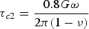 $$\tau _{c2}=\displaystyle{{0.8G\omega } \over {2\pi \lpar 1 - \nu \rpar }}$$
For the migration problem using G = 61 GPa, ν = 0.38, and ω = 13.5°, we find the critical shear stress τc2 is equal to 2.95 GPa. Using the theoretical stress concentration factor we predict maximum stress to be approximately 1.5 GPa. The corresponding shear stress should be approximately 750 MPa assuming Schmid factor to be 0.5. This stress value falls between the lower and upper bound for stable interface motion. Recent literature[Reference Kumar, Li, Haque and Gao10] indicates absence of stress concentration in nanoscale thin films. This has been attributed to stress homogenization due to grain rotation as deformation mechanism. Assuming the absence of stress concentration, we still obtain a stress value of 290 MPa above which grain growth started. This value is higher than 234 MPa for 15 nm grain size and 30° misorientation. We can now clearly state that among all the different grain growth mechanisms, grain growth observed in the current set of experiments is due to stress-induced shear deformation.[Reference Cahn, Mishin and Suzuki20, Reference Winning, Gottstein and Shvindlerman21]
To qualitatively understand the grain growth mechanism, we sorted through different grain growth mechanisms. The motion of planar low- and high-angle grain boundaries under the influence of a mechanical stress field can be attributed to the movement of grain boundary dislocations, which comprise the structure of the boundary.[Reference Winning, Gottstein and Shvindlerman21, Reference Winning, Gottstein and Shvindlerman22] Sansoz and Dupont[Reference Sansoz and Dupont23] proposed that the grain growth results from grain rotation of nano grains and propagation of shear bands. In the current study, most of the grains are nano grains (10–15 nm). We observed discontinuous grain growth. We did not see any shear bands. Although grain rotation is not directly observed yet it cannot be ruled out since significant experimental evidence[Reference Kumar, Li, Haque and Gao10] exists for grain rotation at nanoscale. The conventional plastic deformation mechanism at the notch or crack tip involves emission of dislocations.[Reference Horton and Ohr24, Reference Zielinski, Lii and Gerberich25] These dislocations create an inverse stress intensity factor at the notch/crack tip and reduce the stress concentration. Since grain boundaries are primarily ensemble of discrete dislocations they interact with the notch-induced stress. We propose that dislocation and hence grain boundaries move away from the notch/crack tip under the influence of this stress resulting in grain growth. This explains the grain growth observed at the notch tip but we did see the grain growth away from the notch. Grain growth away from the notch tip is discontinuous grain growth; large grains are getting bigger. These bigger grains are surrounded by randomly oriented extremely small (5–10 nm) grains. Polycrystalline specimens with randomly oriented grains tend to develop micro strain at the grain boundaries due to geometrical incompatibility under applied axial stress. The micro strain is relaxed by having geometrically necessary dislocations (GNDs) at the grain boundary. For nano grains GND-based strain relaxation is not feasible since they cannot accommodate dislocations. However, larger grains can sustain GND-based relaxation. Applied axial loading when coupled with micro strain results in dislocation generation and subsequent dislocation-mediated grain boundary motion. From Fig. 3, we clearly observe some dislocation pileups in grains that are merging. We also observed some step-like features left behind by moving grain boundary resulting in merged grains. From quantitative results and qualitative observation, we can deduce that grain growth observed in the current work is due to shear deformation-induced grain boundary migration. Furthermore, grain growth can be attributed to maintaining geometrical compatibility, which can essentially be termed as geometrically necessary grain growth. Grain rotation is a deformation mechanism responsible for alleviating grain-level stress heterogeneity or incompatibilities. It does not influence grain growth, even though both mechanisms require significant grain boundary (GB) mobility. For extremely small grain sizes, both the GB energy and GB mobility are very high and grain growth is feasible. However, as the grain sizes grow, they lose mobility as a cubic function of grain size and grain growth stops to give up for grain rotation.
In our previous study, we showed how grain rotation could mitigate stress concentration. In this study, though, the grain size is so small that grain rotation does not take place (as evident from the in situ TEM). Grain rotation as primary deformation mechanism has been reported only for grain sizes above 40 nm whereas in the current study the average grain size is ~10 nm. At this grain size grain rotation is found to be minimal. A clear demarcation between different deformation mechanisms has been reported.[Reference Kumar, Alam, Connell and Haque12] For a grain size smaller than 40 nm grain growth is the primary deformation mechanism and above this grain size grain rotation becomes predominant and is followed by dislocation-based plastic deformation at and above ~80 nm.[Reference Kumar, Alam, Connell and Haque12] Average grain size in the present study is ~10 nm and at this grain size grain rotation may not be able to account for geometrical incompatibilities and results in geometrically necessary grain growth as a primary deformation mechanism. Furthermore, we did not observe any significant grain contrast changes over the entire range of stress values and only grain growth is observed. This clearly supports the hypothesis proposed in this study.
In conclusion, we carried out an in situ TEM single edge notch tensile test on freestanding nanocrystalline platinum thin films. Single edge notch specimen is selected to understand the effects of stress concentration on deformation behavior. We found that grains located at the notch tip are found to show significant grain boundary motion and grain growth. There is some growth slightly away from the notch tip also. Some of the grains are found to grow 300% of their original area. From quantitative measurements we find that rapid grain growth occurred above 290 MPa of far field stress and ~0.14% elongation. This value is found to be higher than required for stable interface motion but lower than the stress required for unstable grain boundary motion. Growing grains are found to have remnant dislocations as well as steps from grain boundary migration. This behavior correlates very well with the dislocation model of grain boundaries resulting in grain boundary motion under applied stress.
Supplementary materials
For supplementary materials for this article, please visit http://dx.doi.org/10.1557/mrc.2013.15