Introduction
In recent times, triboelectric nanogenerators (TENGs) have attracted exceptional attention after its first report by Prof. Wang's group in 2012[Reference Fan, Tian and Lin Wang1] presenting its simple, robust, low-cost, and high efficiency for energy harvesting. TENGs generate electricity converting the mechanical motions through the coupling of triboelectrification and electrostatic induction.[Reference Fan, Tang and Wang2,Reference Zhang, Yang, Su, Chen, Hu, Wu, Liu, Wong, Bando and Wang3] TENGs have four basic operating modes[Reference Wang4–Reference Yang, Zhang, Chen, Jing, Zhou, Wen and Wang6] which include vertical contact–separation mode, lateral sliding mode, single-electrode mode, and freestanding triboelectric layer mode. In general, TENGs are primarily composed of positive and negative triboelectric layers with electrodes transporting the charges. Materials for triboelectricity occurrence are selected based on the triboelectric series,[Reference Wang4] further away the materials are separated apart from each other in the series, the greater the charge transfer. The surface charge transfer resulting from the periodic contact separation between these two dissimilar triboelectric materials determines the energy conversion of a TENG.
While TENGs have been demonstrated as sustainable power sources for autonomous applications,[Reference Fan, Tang and Wang2] the output power is a major concern owing to its high voltage and low current. Until now, the electric output of TENGs has been improved up to ~500 W/m2 with a complex device structure.[Reference Fan, Tang and Wang2] According to previous studies,[Reference Byun, Lee, Cho, Nam, Shin and Park7–Reference Van Ngoc and Kang10] enhancement of output performance can be achieved by material modification, increasing the contact area or surface functionalization. The intrinsic properties of the triboelectric materials are critically important for the improvement of TENGs output.[Reference Mahmud, Lee, Kim, Lim and Choi11] With a contact–separation structure, the key technique to enhance the output performance is to increase the surface charge density to achieve a high output performance of TENGs.
Considering high density of triboelectric charges was transferred at each contact, intrinsic parameters such as work functions, dielectric thickness, and the separation distance between the two materials are very important to achieve high surface charge density. Previous reports on increasing surface charge density by nanoparticle synthesis,[Reference Niu, Wang, Yi, Zhou and Wang12] ion injection,[Reference Yu and Wang13] and multi dielectric layer structure[Reference Wanchul Seung, Yoon, Yun Kim, Ryu, Kim, Lee, Hwan Lee, Kim, Kwon Park and Jun Park14] have been investigated but decreases rapidly over time and must be regenerated at each contact. There have been a few related studies on effective charge density increase with a simple fabrication method[Reference Mahmud, Lee, Kim, Lim and Choi11,Reference Wang, Xie, Niu, Lin, Liu, Zhou and Wang15–Reference Feng, Zheng, Zhang, Wang, Zhou and Liu17] but still the charge accumulation and retention in thin film dielectric layers remain critical issues[Reference Villeneuve-Faure, Makasheva, Boudou and Teyssedre18,Reference Li, Su, Kuang, Pan, Zhu and Wang19] for achieving TENGs as sustainable power sources.
The current work focuses on increasing surface charge density by devising a flexible composite structure with an inclusion of a charge accumulation layer for TENG applications. With a contact–separation TENG mechanism, the composite structure consists primarily of a charge accumulation layer, charge retention substrate, and an electrode to efficiently transport charges with the counter electrode. The charge accumulation layer creates negative triboelectric charges on contact with a positive triboelectric material. Polytetrafluoroethylene (PTFE) is chosen as the charge retention substrate owing to its impressive triboelectric properties, importantly, high electronegativity, flexibility, and versatility to simple fabrication. A thin film Parylene-C (PaC) was deposited to accumulate and retain the charges obtained from the triboelectrification process, allowing the acceptance of more charges from an electrode and thereby increasing the output performance. It has been used in a wide range of applications, particularly as a protective coating for biomedical devices and microelectronics.[Reference Lo and Tai20] Its desirable properties include chemical inertness, conformal coating, and excellent barrier properties.[Reference Kahouli, Sylvestre, Ortega, Jomni, Yangui, Maillard, Berge, Robert and Legrand21] The investigation of output stability through a cyclic contact separation mechanism provides better understanding of the charge dissipation on the dielectric surface. The output voltage performance was enhanced by a factor of sevenfold (120 V from the initial 17 V). Furthermore, the influence of charge accumulation at the interface on the electrical output performance is optimized, the V oc increases from 24 to 262 V as the PaC thickness decreases from 10 to 0.5 µm, giving a tenfold enhancement. The use of an organic material like PaC as a triboelectric charge accumulation layer provides many advantages (i) with a reduced fabrication time leading to cost effective compared with the existing TENG reports,[Reference Mahmud, Lee, Kim, Lim and Choi11,Reference Song, Kuang, Panwar, Yang, Danny, Tjin, Ng, Majid, Zhu, Yong and Wang22] which involves micro patterning, material processing; (ii) a high electrical output performance with an increased work function difference of ϕ PaC = 3.27 eV, ϕ PTFE = 5.6 eV, and ϕ Cu = 4.5 eV; (iii) long cycle life with very high-dielectric strength (6800 V/mil)[Reference Access, Heid, Stett and Bucher23]; (iv) thin thickness with pin-hole free conformability, and (v) highly compatible with various friction-related applications.[Reference Genter and Paul24] By this technique, the effective surface charge density improved from 0.5 to 70.2 µC/m2, which is 140 times greater than the initial results demonstrating the increased output performance.
Materials and methods
Device fabrication
The process of the charge accumulation layered TENG begins by the deposition of PaC on the 100 µm PTFE sample. PaC was deposited through a vapor deposition polymerization process onto the PTFE substrate. The process begins with a raw powdered dimer DPX-C 980130-C acquired from Specialty Coating Systems in the solid state being placed into the aluminum loading boat, which is then inserted into a vaporizer. The raw dimer is heated to 135 °C. At this time, the vapor is pulled, under vacuum into the furnace and heated to very high temperature up to 690 °C which allows for sublimation and the splitting of the molecule into a monomer. The monomer gas continues to be drawn by vacuum onto the PTFE sample at ambient temperatures in the coating chamber. The final stage of the PaC deposition process is cold trap. The cold trap is cooled to between –90 and –120 °C and is responsible for removing all residual PaC materials pulled through the coating chamber. An ultra-thin PaC film was deposited over the PTFE using an SCS Lab coater 2 with Silane A174 present in the chamber to act as an adhesion promoter. A thorough understanding of the process is key to control thickness and ensure a successful coating cycle.
Electrical measurement
To achieve repeatable and stable output characteristics, an Instron 3365 traction system was used to control the speed and displacement of the TENG. A constant displacement of 7 mm, 50 N contact force, and speed of 20 mm/s was fixed for investigating the output performance. The output signals of the charge accumulation layered TENG were measured using a Keithley 2636 sourcemeter and Agilent 4288A capacitance meter controlled by using a LabVIEW program.
Capacitance measurement
The capacitance of the thin film charge accumulation layer was measured. The setup includes the PaC charge accumulation layer (30 mm × 30 mm sample size) sandwiched in between two copper electrodes to form a metal–insulator–metal MIM. The two copper electrodes on the top and bottom of a sandwich structure are connected by two electrical terminals that connect it to the rest of the circuit. One end of the structure connects to source and the other connects to ground. The capacitance was measured using an Agilent 4288A capacitance meter which can measure between 100 kHz and 1 MHz (4-point probes) with bare minimum parasitic noise. The system was a controlled by a custom-developed LabVIEW interface. A comparative measurement is performed on both PTFE and PaC charge accumulation layer inclusion on the PTFE layer. All devices on each sample were measured and compared with in-depth analysis.
Work function determination
Material work functions were measured using a KP Technology Kelvin probe system. Kelvin probe is a non-contact and non-destructive vibrating capacitor technique to measure the work function difference between two surfaces, determined by vibrating the reference surface above the test sample and adjusting voltage until a zero or null output results. The work function of the test materials was measured by comparison with a known work function value of a gold vibrating tip by approaching to 300 gradients on a small scan area of 5 mm × 5 mm at 72 Hz frequency and 10 V amplitude for 50 single point scans, measuring the contact potential difference (CPD) and calculating the work function of the unknown materials.
Experimental setup
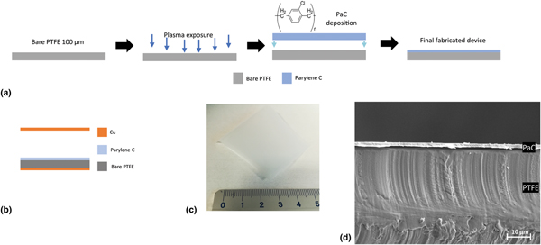
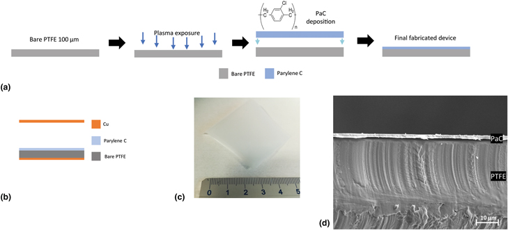
An effective charge accumulation flexible composite triboelectric layer for increasing surface charge density was fabricated. The triboelectric layer film consists of a thin charge retention flexible triboelectric layer and the detailed fabrication process schematic is presented in Fig. 1(a) with schematic and fabricated device in Figs. 1(b) and 1(c).
Structure and fabrication process of the charge accumulation layered TENG. (a) Fabrication process flow of TENGs. (b) Schematic diagram of charge accumulation layered TENG. (c) Optical image of the fabricated TENG. (d) Cross-sectional SEM image with 4 µm thickness PaC deposited on PTFE sample structure.

A thin film PTFE from Goodfellow Ltd., 100 µm was used as a substrate for its excellent triboelectric property, high electron affinity and high-dielectric strength with dimensions 30 mm × 30 mm. This was followed by deposition of PaC charge retention layer to increase the device stability for long-term operation and increase the surface charge density. It is worth noting that PaC has been extensively used in electret system to retain charges over a long period of time for micro-energy harvesting applications.[Reference Wada, Hamate, Nagasawa and Kuwano25] With a high-dielectric constant of 3.15, charge carrier densities larger than 2.0 mC/m2 can be achieved making PaC a material offering several attractive features.[Reference Genter and Paul24] A traction machine from the Instron system was used to investigate the contact–separation output performance of the TENG controlled by a homemade LabVIEW program to simultaneously record electrical performances. Scanning electron microscopy (SEM) image of the flexible composite triboelectric layer with a PTFE thin film with a PaC charge accumulation layer morphology and microstructure is shown in Fig. 1(d).
TENG working mechanism
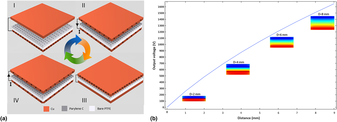
The charge transfer mechanism of the effective charge accumulation layered TENGs to increase the surface charge density by cyclic contact–separation mode is illustrated in Fig. 2(a). Periodic contact and separation between two materials with different triboelectric polarities drives electrons back and forth through an external circuit due to the coupling of the triboelectrification and the electrostatic induction.[Reference Fan, Tian and Lin Wang1] The charge transfer mechanism between the contacting materials depends on their triboelectric series position, electron affinities, and work function. The copper (Cu) foil as the top electrode is connected to the bottom electrode in an open circuit configuration. Initially, before the contact of the triboelectric layers (i.e., PaC and Cu), there exists a neutrality without any external force, hence no electrical potential difference (I). A vertical force is induced resulting in a physical contact between the two triboelectric layers (II). At this instance, equal and opposite charges (−Q and +Q) are created owing to triboelectrification/contact electrification (i.e., the electrons are injected from PaC into Cu, resulting in negative charges on the surface of the PaC and positive charges on the surface of Cu). The additional charges created are accumulated at the interface of PaC–PTFE layer. Contact-induced charges generate a potential drop when the two surfaces are separated by a mechanical force (III). The presence of the PaC increases the triboelectric surface charge at the contact interface owing to its work function difference between the Cu and PaC and increases the material charge storage capacity at the PaC interface PTFE layer. The work function acts as a driving force for the triboelectric charge generation. When the charged layered TENGs were released (IV), a potential difference between the top electrode and the bottom electrode became apparent due to an electrostatic induction process. The electrons are pumped back from the bottom to the top electrode to become neutral through an external circuit reaching its initial state. Continuous contact separation process results in increasing output performance validating the charge accumulation and generating a complete cyclic alternating current (AC) output potential discussed in the “Results and discussion” section.
(a) Working mechanism of contact–separation TENG. (I) Initial position with a 7 mm gap. (II) Vertical force makes the top electrode closer to the charge accumulation layer. (III) Charge accumulation layered TENG in contact generating positive triboelectric charges on the copper side and negative charges on the PaC surface. (IV) Separation between electrodes driving current in the external circuit. (b) Finite-element simulation of the potential distribution in the TENG under the different gap distances of the electrodes at a charge density of 10 µC/m2.

To obtain a more quantitative understanding of the power generation mechanism, we establish a theoretical model of a TENG to simulate the electric potential distribution using COMSOL Multiphysics software during the displacement of the top electrode. In this model, the active tribo material is the PaC layer with 4 µm thickness and the electrode layers are made of Cu. The top electrode displaces in the process while the bottom electrode is fixed and connected to the ground respectively. Figure 2(b) shows the electrical potential generated between electrode changes when the moving electrode displaces from the friction layer. The inset color figures show the simulated electric potential distribution when the moving electrode displaces with a gap distances from 0 to 9 mm with increase in the open circuit voltage reaching a maximum of 1.6 kV.
Results and discussion
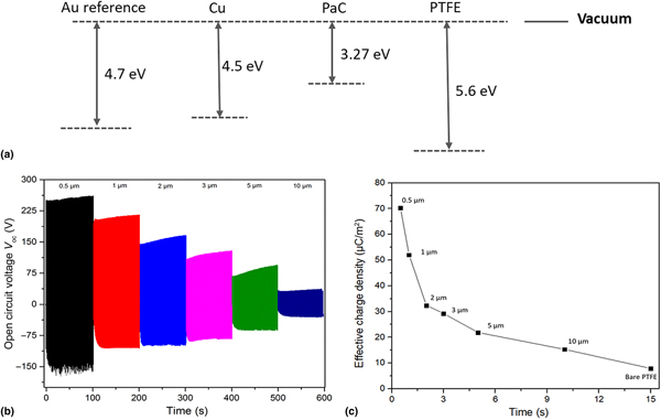
Material work function (ϕ) provides a better understanding toward the charge transfer process. The triboelectric charge density depends on: (i) the work function difference between the two materials in contact, (ii) the dielectric constant, and (iii) structural parameters (i.e., dielectric thickness and separation distance during triboelectric process). Figure 3(a) shows the work functions of the material surfaces and have been determined by the measurement of their contact differences of potential with respect to gold reference surfaces of known work function (ϕ Au = 4.7 eV) using the Kelvin probe technique. During our experiments, enhancement of triboelectric charge density was observed when the work function difference maximized, and the dielectric thickness minimized.
TENG output performance. (a) Measured work function using kelvin technique. (b) Output performance as a function of PaC thickness. The influence of PaC decreases from 10 to 0.5 µm, the open circuit voltage (V oc) increases from 24 to 262 V, giving a tenfold enhancement. (c) Effective charge density increases from 0.5 to 70.2 µC/m2 with increasing thickness.
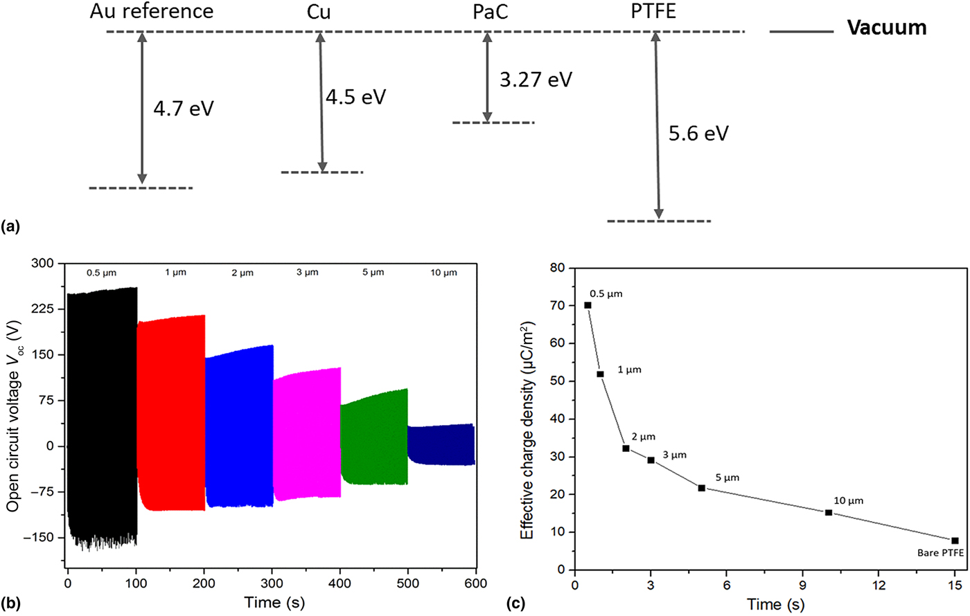
To evaluate the performance of charge accumulation layered TENGs, a modified Instron mechanical system controlled by the LabVIEW program was used to alter the speed and displacement of the TENG. The output open-circuit voltage (V oc) was measured for the cyclic contact–separation mechanism at 20 mm/s with an operating distance of 7 mm. The triboelectric layer made of a PaC charge accumulation layer has negative triboelectric charges on the surface and attracts positive counter charges to the electrodes. When the PaC layer comes in contact with the counter electrode, positive charges are formed on the corresponding electrode. The PaC layer constantly displaces in the contact–separation mechanism, the positive charges are repeatedly transferred between the two electrodes, resulting in AC output.
Figure 3(b) illustrates the influence of PaC thickness varied between 0.5 and 10 µm to determine its electrical output performance. Considering identical initial surface potentials, when the PaC layer thickness decreases from 10 to 0.5 µm, the V oc increases from 24 to 262 V, giving a tenfold enhancement. This is explained by the charge migration at lower PaC thickness and storage at the interface of PTFE and PaC layers. The voltage increases with a decrease in PaC thickness owing to higher charge storage at the interface and resulting in a faster charge transfer mechanism with higher charge density. The 0.5 µm PaC layer proved to perform with higher electrical output but it is the 4 µm PaC that performed with better balance between both charge accumulation and retention characteristics.
The surface charge Q is defined by its capacitance C in the parallel plate structure and its resulting output voltage V:
 $$Q = CV$$
The capacitance of the thin film charge accumulation layer TENG was measured. The capacitance of the charge accumulation layer sandwiched between two copper electrodes to form MIM is measured at 1 kHz by using a capacitance meter. A comparative measurement is performed on both bare PTFE and PaC charge accumulation layer inclusion on the PTFE layer.
Figure 3(c) shows the effective surface charge density improved from 0.5 to 70.2 µC/m2, which is 140 times of the effective charge density with 0.5 µm thickness PaC, this value is comparable or higher than the other reported charge densities of TENGs[Reference Li, Su, Kuang, Pan, Zhu and Wang19,Reference Ma, Jie, Bian, Li, Cao and Wang26,Reference Lin, Cheng, Lee, Pradel and Wang27] which follow complex processing. With the continuous triboelectrification process, acceptance of more charges from the electrodes increases the transferred charges, thereby increasing the effective charge density. This increase of effective charge density will greatly improve the output current, voltage, and power of the TENGs used for real-time applications such as sensors,[Reference Fan, Lin, Zhu, Wu, Zhang and Wang28] as well as autonomous power sources.[Reference Hsieh, Hsu and Chen29] With contact separation mode TENG, the varying capacitance C with respect to its distance d of the effective charge accumulation layer is given by
 $$C = \displaystyle{{\varepsilon \cdot A} \over d}$$
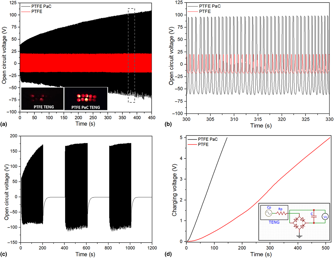
where the active triboelectric layer consists of thin layer PaC adhered to 30 mm × 30 mm PTFE sample on a copper electrode while the other consists of a copper substrate connected to the measurement unit. PTFE, a material with high electron affinity, shows a better capability of trapping charges over long period. The effect of PaC layer on PTFE shows a good prospect in increasing the charge density and enhances the contact electrification process. As the top copper electrode approaches the PaC triboelectric layer, the surface polarization reduces by driving the positive charges from the bottom Cu electrode to the top electrode. While the residual polarization present in PaC will enhance the consecutive triboelectric charge transfer mechanism leading to increase in the charge density. Given the same amount of charges (ΔQ) transported back and forth, a faster contact–separation process is expected to produce larger current peaks (I sc = ΔQ/Δt) than that during the slower separation and increase the charge accumulation. A comparative electrical response of bare PTFE and charge accumulation layer inclusion on PTFE open circuit voltage under the contact separation TENG mechanism is presented in Fig. 4(a) with enlarged curves in Fig. 4(b). With a continuous triboelectrification process at 20 mm/s, acceptance ability of more charges from the electrodes increases the transferred charges, thereby increasing the output voltage. A bare PTFE reached 17 V but explicitly increases to reach 120 V after the inclusion of the 4 µm PaC as a charge accumulation layer, indicating an enhancement of seven times with the charge accumulation layer. The surface charges migrate through the thin film PaC layer and are stored at the interface between the PTFE and PaC layers. Thus, the PaC layer allows the accumulation of the charges generated by triboelectrification and to refill the charges on every contact. The charges initially on the surface are thus permanently accumulated/stored at the interface. This increase of stored charges permits higher charge transfer between the electrodes, thus increasing the electrical output performance of TENGs. The inset photographs shows ten LEDs in series illuminated by a TENG before and after the PaC charge accumulation layer, illustrating an important scale improvement in illumination. (Supplementary material S1 illustrates the influence of cycling speed on the output performance. It is clear that higher the speed generates higher the charge transfer resulting in an enhanced charge accumulation.)
Electrical characterization of the 4 µm charge accumulation layered TENG. (a) Comparison of TENGs output voltage characteristics. The inset shows ten series connected red LEDs illuminated by TENGs. (b) Enlarged view of the output voltage comparison between a bare PTFE and charge accumulation layered TENGs. (c) Cyclic output voltage stability of TENG working intermittently for 15,000 cycles at 20 mm/s. (d) The charging process of a 10 µF capacitor up to 5 V through a bridge circuit under different triboelectric layers. The inset shows the equivalent circuit.
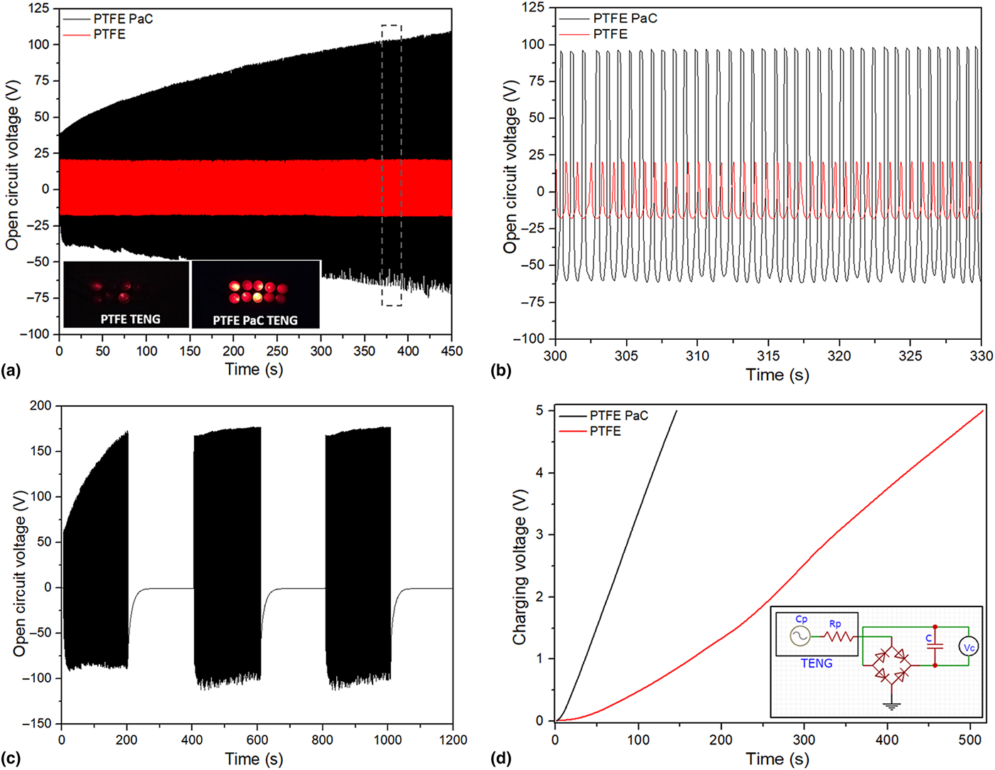
To demonstrate the device reliability and charge retention characteristics of the charge accumulation layered TENG, the open-circuit voltage was measured during the continuous ON–OFF cycles for 1200 s presented in Fig. 4(c) proving no decline is observed after a long-term continuous operation. In the initial 50 s, the material charges rapidly from the contact separation mechanism and reaches a V oc saturation of 160 V and remains stable until the continuous operation for 200 s. After a hold time of 200 s, the open circuit voltage is still maintained at 160 V. The result validates to conclude that the charges are well retained during the OFF period, the maximum voltage holds steadily despite intermediate stops. Thus, the charge accumulation layer accumulates charges during the ON time and maintains the charge retention during the OFF time. Periodic tests are continued until 1200 s evidencing the device stability of the charge accumulation layer inclusion for high-performance TENG applications.
To validate the performance of the charge accumulation layered TENG, an experiment for capacitor charging was conducted. Figure 4(d) shows the charging voltage versus time signals of a capacitor charged to 5 V on a 10 µF capacitor. The charge accumulation layered TENG was connected to charge a capacitor (10 µF) through a bridge circuit, as shown by the equivalent circuit in the inset of Fig. 4(d). The AC output of the TENG was rectified to DC output through the bridge circuit. A comparative charge analysis was performed between a bare PTFE and charge accumulation layer included PTFE. The charge accumulation layered TENG rapidly charges in around 100 s outperforming the bare PTFE which requires more than 500 s to reach 5 V. The charge accumulation layered TENGs charging time is five times much faster than the bare PTFE demonstrating the charge accumulation layered TENGs viability for use in a wide array of smart applications as well as to effectively increase the output performance.
Conclusion
In summary, the charge accumulation layer inclusion structure to increase the surface charge density using PaC layer for TENGs has been developed successfully. Owing to the excellent friction and mechanical properties of the PaC structure, the output voltage performance was enhanced by a factor of sevenfold (120 V from the initial 17 V). Furthermore, the influence of charge accumulation at the PaC PTFE interface on the electrical output performance is optimized, the V oc increases from 24 to 262 V as the PaC thickness decreases from 10 to 0.5 µm, giving a tenfold enhancement.
By this technique, the effective surface charge density improved from 0.5 to 70.2 µC/m2, which is 140 times greater than the initial results demonstrating the increased output performance. Considering these merits of simple fabrication, increased performance, robust characteristics, and cost-effective technology, we believe that effective charge accumulation layer included TENGs make it attractive for charging applications for wearables/portable electronics.
Supplementary material
The supplementary material for this article can be found at https://doi.org/10.1557/mrc.2019.64
Acknowledgments
This research was supported under the AMPEERS-2 project by the theme “Networks and energy storage”. The authors thank Thierry CAMILLIONI for the Instron setup and Jessica MAZUIR for advice in preparation of cross section sample for imaging by SEM.