Introduction
A block copolymer (BCP) is a polymer that is made up of blocks of chemically distinct monomers. For example, a polystyrene-block-polymethylmethacrylate (PS-b-PMMA) BCP consists of a PS chain covalently bonded to a PMMA chain. If the blocks are immiscible, the BCP can self-assemble into periodic nanostructures with dimensions ranging from a few nanometers to several 100 nanometers.Reference Bates and Fredrickson1–Reference Nunns, Gwyther and Manners5 The phase-separated structure consists of “microdomains” of each block whose geometry depends on the volume fraction of the block and whose periodicity depends on the length of the polymer chain.Reference Hillmyer6 The periodicity of the structure can range from a few nanometers to hundreds of nanometers.
A rich variety of nanostructures can be self-assembled based on the intrinsic properties of the blocks and the microdomain geometry, which is influenced by the polymer architecture, the annealing process (e.g., annealing by exposure to a solvent vapor environment or to an elevated temperature), and constraints such as those imposed by a patterned substrate.Reference Cheng, Ross, Smith and Thomas3,Reference Sinturel, Vayer, Morris and Hillmyer7 BCPs with two chemically distinct blocks (e.g., diblock copolymers [Figure 1a–c]) or three (e.g., triblock copolymers) or three (e.g., triblock terpolymers) chemically distinct blocks are most commonly used, but incorporating further blocks and various architectures such as linear, star, cyclic, or brush copolymers brings more diversity to both the properties and the morphology of the resulting self-assembled structure (Figure 1d).Reference Bates, Hillmyer, Lodge, Bates, Delaney and Fredrickson8
Schematics of block copolymer (BCP) self-assembly. (a) Self-assembled morphology of a diblock copolymer and the morphology revealed after etching one block. (b–d) Representative structures from BCP self-assembly. (b) Lamellae; (c) cylinders, both from a diblock copolymer; (d) Archimedean tiling from a star terpolymer.

BCPs can be used in a wide range of applications,Reference Schacher, Rupar and Manners9,Reference Yoo, Byun, Jeong and Lee10 constituting functional materials themselves by virtue of the properties of the blocks, or by selectively etchingReference Choi, Gwyther, Manners and Ross11 one block to form masks or templates for the synthesis of functional materials. BCPs can include organic coil-like blocks, liquid-crystalline blocks, Si- or metal-containing blocks, biological blocks, or conductive blocks, thereby providing a multitude of properties.Reference Kulbaba and Manners12–Reference Ross, Jung, Chuang, Ilievski, Yang, Bita, Thomas, Smith, Berggren, Vancso and Cheng15 The BCP nanostructure can be altered by several chemical methods such as sequential infiltration synthesis (SIS), which introduces metals or oxides from a precursor as in chemical vapor deposition,Reference Peng, Tseng, Darling and Elam16 by salt complexation,Reference Kim, Misner, Yang, Gang, Ocko and Russell17 or by nanoparticle incorporation.Reference Zhao, Thorkelsson, Mastroianni, Schilling, Luther, Rancatore, Matsunaga, Jinnai, Wu, Poulsen, Fréchet, Alivisatos and Xu18
Many of these applications are based on thin films of BCPs, and one of the most widely studied applications is in nanoscale lithography, where one block is removed by etching, and the other is used as a mask to define features in a microelectronic device (Figure 1a). In this article, we will first discuss the applications of thin-film BCPs in lithography and other fields where a two-dimensional (2D) nanopatterned structure is required. We will then discuss three-dimensional (3D) BCP assemblies. We show that BCP nanostructures have applications in fabrication of integrated circuits,Reference Yi, Bao, Tiberio and Wong19,Reference Black, Ruiz, Breyta, Cheng, Colburn, Guarini, Kim and Zhang20 magnetic storage media,Reference Xiao, Yang, Edwards, La and Nealey21–Reference Cheng, Ross, Tsui and Russell23 sensors,Reference Guenther, Kuckling, Corten, Gerlach, Sorber, Suchaneck and Arndt24,Reference Jeong, Jin, Ahn, Park, Yoo, Koo, Choi, Kim and Lee25 photonic crystals,Reference Kang, Walish, Gorishnyy and Thomas26 photovoltaics,Reference Zhang, Cirpan, Russell and Emrick27 and separation membranes,Reference Metz, Potreck, Mulder and Wessling28 as well as for making 3D nanostructures.Reference Ross, Berggren, Cheng, Jung and Chang4
BCPs for nanolithography
In nanolithography, a film of a BCP is prepared on a substrate, and one of the blocks is removed. The remaining structure serves as a mask for pattern transfer into a metal, dielectric, or other material. This can be carried out using the microdomain pattern made from an untemplated BCP film, producing a dense array of dots, holes, or lines without long-range order. However, the greatest efforts have been expended in developing BCP nanolithography for nanoscale electronic devices, where precise registration and reproducibility of the self-assembled nanostructures and low defect levels are essential. Conventional 193-nm wavelength photolithography feature sizes are limited by diffraction, although sublithographic feature sizes may be obtained by complex double or quadruple patterning processes.Reference Fonseca, Somervell, Scheer, Kuwahara, Nafus, Gronheid, Tarutani, Enomoto, Dusa and Conley29 However, 193-nm lithography does not produce features below about 20-nm dimensions, and directed self-assembly (DSA) of BCPs has become a candidate planar process for semiconductor device nanofabrication, according to the International Technology Roadmap for Semiconductors.
The period of the microphase-separated BCP structure is governed by the polymer chain length and hence the degree of polymerization, N (the number of monomers constituting the chain), but the driving force for self-assembly is governed by the product χN, where χ is the Flory–Huggins interaction parameter quantifying the incompatibility between the blocks. Therefore, high χ is desirable to obtain features with small period from BCPs with low N. BCPs that yield a feature period below 10 nm can microphase-separate at room temperature if χ is high enoughReference Sinturel, Bates and Hillmyer30 or by design of the macromolecular architecture (such as brush BCPs). This makes BCP lithography an attractive path to continued device miniaturization.
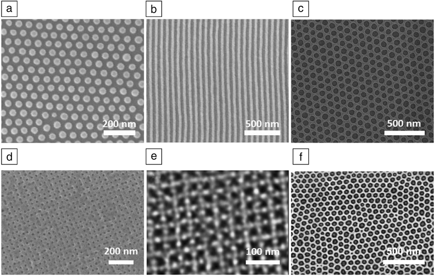
BCP thin films can be spin-coated from solution like a resist layer, annealed using a hotplate at moderate temperatures or by placing them in a solvent vapor, and etched by reactive ion etching (RIE), making them compatible with conventional semiconductor fabrication technology.Reference Kim, Park and Hinsberg31,Reference Delgadillo, Gronheid, Thode, Wu, Cao, Neisser, Somervell, Nafus and Nealey32 Diblock copolymer films on unpatterned substrates form periodic morphologies after annealing, consisting of close-packed spheres, in-plane or out-of-plane-oriented cylinders or lamellae, perforated lamellae, or gyroids, by controlling the block volume fractionReference Bates and Fredrickson1 and the annealing process (Figure 2a–c).Reference Sinturel, Vayer, Morris and Hillmyer7,Reference Bai, Hannon, Gotrik, Choi, Aissou, Liontos, Ntetsikas, Alexander-Katz, Avgeropoulos and Ross33
Representative scanning electron microscope images of thin-film self-assembled block copolymer (BCP) structures. (a) Monolayer of spheres; (b) in-plane cylinders; (c) perforated lamellae; (a–c) are from a diblock copolymer. (a–c) Reproduced with permission from Reference Reference Bai, Hannon, Gotrik, Choi, Aissou, Liontos, Ntetsikas, Alexander-Katz, Avgeropoulos and Ross33. © 2014 ACS Publications. (d) Square array of holes from a linear triblock terpolymer blended with a homopolymer. Reproduced with permission from Reference Reference Choi, Gwyther, Manners and Ross11. © 2012 ACS Publications. (e) Archimedeam tiling pattern, from a three-miktoarm star terpolymer blended with a homopolymer. Reproduced with permission from Reference Reference Aissou, Choi, Nunns, Manners and Ross34. © 2013 ACS Publications. (f) Hierarchical nanostructure from a blend of a silicon-containing BCP and an iron-containing BCP. Reproduced with permission from Reference Reference Park, Kim, Jeong, Kim, Yoo, Hur, Kim, Thomas, Alexander-Katz and Jung35. © 2013 Nature Publishing Group.
More diverse morphologies can be produced from tri-BCPs (or multi-BCPs),Reference Bates, Hillmyer, Lodge, Bates, Delaney and Fredrickson8,Reference Aissou, Choi, Nunns, Manners and Ross34 mixtures of di-BCPs,Reference Park, Kim, Jeong, Kim, Yoo, Hur, Kim, Thomas, Alexander-Katz and Jung35 or multi-BCPs blended with a homopolymer.Reference Choi, Gwyther, Manners and Ross11 For example, square arrays were achieved by using triblock terpolymer/homopolymer blends (Figure 2d),Reference Choi, Gwyther, Manners and Ross11 Archimedean tiling patterns were produced from a three-miktoarm star terpolymer (a star-shaped polymer where three different polymer arms emanate from a core) (Figure 2e),Reference Aissou, Choi, Nunns, Manners and Ross34 and blended morphologies between spheres and perforated lamellae were demonstrated by blending a Si-containing BCP with an iron-containing BCP (Figure 2f).Reference Park, Kim, Jeong, Kim, Yoo, Hur, Kim, Thomas, Alexander-Katz and Jung35
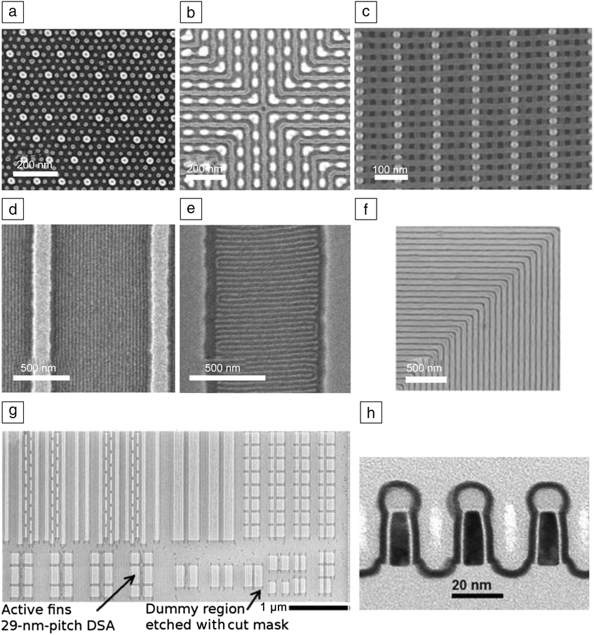
The microdomain patterns formed in thin films of BCPs possess short-range order, but lack long-range order, as seen in some of the images in Figure 2. A top-down method can be employed to guide BCP self-assembly, providing registration and alignment with features in the substrate, and minimizing the defectivity. Graphoepitaxy and chemoepitaxy are the two main templating strategies for DSA,Reference Cheng, Mayes and Ross36–Reference Mansky, Liu, Huang, Russell and Hawker40 using physical confinement to direct the arrangement of the polymer chains and interfacial interactions to induce preferential wetting by the polymer chains, respectively, to control BCP self-assembly. This can produce well-ordered periodic arrays as well as aperiodic structures not found in bulk.Reference Wu, Cheng, Katsov, Sides, Wang, Tang, Fredrickson, Moskovits and Stucky41–Reference Luo and Epps43 Topographical templates for graphoepitaxy include small posts fabricated by electron-beam lithography, functionalized to be attractive to one block,Reference Tavakkoli, Gotrik, Hannon, Alexander-Katz, Ross and Berggren44 or trenches fabricated by photolithography or interference lithography.Reference Bosworth, Paik, Ruiz, Schwartz, Huang, Ko, Smilgies, Black and Ober45–Reference Segalman, Hexemer and Kramer48 On the other hand, chemoepitaxy templates consist of chemically distinct regions of the substrate that are attractive to one or the other block, such as stripes, bends, dots, and other features.Reference Ruiz, Kang, Detcheverry, Dobisz, Kercher, Albrecht, de Pablo and Nealey49–Reference Cheng, Rettner, Sanders, Kim and Hinsberg51 In both graphoepitaxy and chemoepitaxy, pattern multiplication has been demonstrated (i.e., the density of templating features can be less than the final density of the BCP pattern).Reference Bita, Yang, Jung, Ross, Thomas and Berggren37,Reference Ruiz, Kang, Detcheverry, Dobisz, Kercher, Albrecht, de Pablo and Nealey49 To optimize the templates in order to produce the desired self-assembled BCP geometries, inverse design algorithms combined with self-consistent field theory (SCFT) simulations have been developed, where SCFT can predict the BCP morphologies for different conditions of film thickness, topographic or chemical confinements, and surface energy.Reference Yi, Bao, Tiberio and Wong19,Reference Hannon, Ding, Bai, Ross and Alexander-Katz52–Reference Khaira, Qin, Garner, Xiong, Wan, Ruiz, Jaeger, Nealey and de Pablo54
Figure 3 shows examples of BCP films templated by graphoepitaxy (Figure 3a–e, g–h) and chemoepitaxy (Figure 3f).Reference Yang, Jung, Chang, Mickiewicz, Alexander-Katz, Ross and Berggren55,Reference Jung and Ross56 The scale-up of these processes to the wafer level, using templates made by photolithography, has been demonstrated.Reference Liu, Nealey, Raub, Hakeem, Brueck, Han and Gopalan57,Reference Cheng, Sanders, Truong, Harrer, Friz, Holmes, Colburn and Hinsberg58
Directed self-assembly (DSA) of block copolymers (BCPs). (a–c) Scanning electron microscope (SEM) images of ordered BCP morphology formed within a sparse 2D lattice of posts (brighter dots). (a) Sphere array. Reproduced with permission from Reference Reference Bita, Yang, Jung, Ross, Thomas and Berggren37. © 2008 AAAS. (b) Nested-elbow structures with a cross-point junction in the center. Reproduced with permission from Reference Reference Yang, Jung, Chang, Mickiewicz, Alexander-Katz, Ross and Berggren55. © 2010 Nature Publishing Group. (c) 3D bilayer cylindrical structure. Reproduced with permission from Reference Reference Tavakkoli, Gotrik, Hannon, Alexander-Katz, Ross and Berggren44. © 2012 AAAS. SEM images of cylinders (d) parallel and (e) perpendicular to steps on a trenched substrate. (d–e) Reproduced with permission from Reference Reference Jung and Ross56. © 2007 ACS Publications. (f) Top-down SEM of 90°-angled lamellae from chemoepitaxy of a ternary polystyrene-block-poly(methyl methacrylate)/polystyrene/polymethyl methacrylate blend. Reproduced with permission from Reference Reference Stoykovich, Müller, Kim, Solak, Edwards, de Pablo and Nealey50. © 2005 AAAS. (g) DSA of a lamellar phase BCP to form line-space circuit patterns in order to fabricate Si fin features. (h) Transmission electron microscope image of 29-nm pitch silicon-on-insulator fins formed by BCP DSA. (g–h) Reproduced with permission from Reference Reference Tsai, Pitera, Miyazoe, Bangsaruntip, Engelmann, Liu, Cheng, Bucchignano, Klaus, Joseph, Sanders, Colburn and Guillorn46. © 2014 ACS Publications.
As mentioned previously, a high χ is desirable to obtain microdomains with small dimensions. However, high-χ BCPs usually exhibit large differences in surface energy between the blocks, favoring in-plane orientation of lamellar or cylindrical microdomains. Perpendicularly oriented microdomains provide high-aspect-ratio features that facilitate pattern transfer, and can be promoted by a neutral coating that has equal affinity to both blocks of the polymer chain,Reference Bates, Seshimo, Maher, Durand, Cushen, Dean, Blachut, Ellison and Willson59,Reference Kim, Kim, Lee, Ross and Son60 a comb-like polymer architecture,Reference Hong, Gu, Huh, Sveinbjornsson, Jeong, Grubbs and Russell61 and processing under external conditions, including an electric field,Reference Olszowka, Hund, Kuntermann, Scherdel, Tsarkova and Böker62 magnetic field,Reference Osuji, Ferreira, Mao, Ober, Vander Sande and Thomas63 temperature gradient,Reference Singh, Yager, Berry, Kim and Karim64,Reference Hashimoto, Bodycomb, Funaki and Kimishima65 solvent gradient,Reference Kim, Kim, Lee, Ross and Son60,Reference Cui, Fujikawa, Nagano, Shimokita, Miyazaki, Sakurai and Yamamoto66 shear,Reference Angelescu, Waller, Adamson, Deshpande, Chou, Register and Chaikin67 zone casting,Reference Tang, Wu, Smilgies, Matyjaszewski and Kowalewski68 electrohydrodynamic jet printing,Reference Onses, Ramírez-Hernández, Hur, Sutanto, Williamson, Alleyne, Nealey, de Pablo and Rogers69 or electrospray deposition.Reference Hu, Choo, Feng and Osuji70Figure 4 shows examples of the alignment of BCP microdomains perpendicular to the substrate.Reference Böker, Elbs, Hänsel, Knoll, Ludwigs, Zettl, Urban, Abetz, Müller and Krausch71
Controlling the orientation of microdomains. (a) Perpendicular microdomains from the self-assembly of a brush block copolymer (BCP). Left: schematic. Right: atomic force microscope image. Reproduced with permission from Reference Reference Hong, Gu, Huh, Sveinbjornsson, Jeong, Grubbs and Russell61. © 2013 ACS Publications. (b) The solvent annealing of BCP thin films with a top coat layer to produce perpendicular microdomains. Left: schematic, t A: top coating thickness, t B: BCP film thickness. Right: Scanning electron microscope image of cross-section and top-down view. Reproduced with permission from Reference Reference Kim, Kim, Lee, Ross and Son60. © 2014 Wiley-VCH. (c) Zone casting method to direct the self-assembly of BCPs; Left: schematic. Right: atomic force microscope images and grazing incidence small-angle x-ray scattering (upper left inset) patterns of aligned microdomains. Arrow indicates casting direction. Reproduced with permission from Reference Reference Tang, Wu, Smilgies, Matyjaszewski and Kowalewski68. © 2011 ACS Publications. (d) Electric-field-induced alignment of BCP microdomains. Reproduced with permission from Reference Reference Böker, Elbs, Hänsel, Knoll, Ludwigs, Zettl, Urban, Abetz, Müller and Krausch71. © 2002 APS. (e) The electrospray process of a tri-BCP. Arrows indicate solvent evaporation direction. Reproduced with permission from Reference Reference Hu, Choo, Feng and Osuji70. © 2015 Wiley-VCH.
Pattern transfer from two-dimensional BCP films
In some applications, the BCP film itself forms the functional material, such as a porous dielectric formed by etching a BCP film, but in many cases, the BCP film is used as a sacrificial mask for patterning another material.Reference Hamley72,Reference Tu, Bai, Liontos, Ntetsikas, Avgeropoulos and Ross73 Monolayers of in-plane cylinders or spheres, perpendicular cylinders and lamellae, and perforated lamellae are particularly suitable for pattern transfer. Pattern transfer takes advantage of the methods developed for planar processing, including additive (e.g., liftoff) and subtractive (etching) methods.
Etching an underlying material through a BCP mask allows pattern transfer into many materials, including multilayers or epitaxial structures that cannot be grown on top of the BCP mask.Reference Segalman2,Reference Tu, Bai, Liontos, Ntetsikas, Avgeropoulos and Ross73,Reference Cheng, Ross, Chan, Thomas, Lammertink and Vancso74 RIE or ion-beam etching are typically used, and the BCP pattern may first be transferred into a hard mask such as a heavy metal (Ta, W, etc.) or hard carbon, which has greater durability than the BCP film during the etch of the functional material.
Additive patterning has also been widely applied, including electrodeposition, liftoff, and damascene processes.Reference Xiao, Yang, Edwards, La and Nealey21,Reference Thurn-Albrecht, Schotter, Kastle, Emley, Shibauchi, Guarini, Black, Tuominen and Russell75 Liftoff involves depositing the functional material onto a soluble BCP pattern with vertical or undercut pores, using a collimated vapor deposition process such as evaporation to produce well-defined edge morphologies of the deposited material. Dissolving the BCP pattern removes the material on top of it, leaving only the material that was deposited on the substrate at the bottom of the pores. In a damascene process, the functional material is deposited over BCP topographical features, then etched back and planarized by, for example, RIE. Etching is stopped once it has reached the BCP features, leaving the functional material within the pores of the BCP film.Reference Black, Guarini, Sandstrom, Yeung, Zhang and Moss76
BCP-based routes to three-dimensional nanostructured materials
BCPs can also produce 3D structures, which can be built up from 2D layers, or formed in one step from thick-film or bulk BCPs with multiple layers of microdomains (Figure 5). One class of synthetic routes involves building a 3D functional material from stacks of 2D layers or by repeatedly templating one BCP on another (Figure 5a–c).Reference Ross, Berggren, Cheng, Jung and Chang4,Reference Shin, Mun, Hwang, Yoon, Kim, Yun, Yang, Oh, Lee, Shin, Lee, Park, Kim and Kim77 Independent BCP layers can be stacked by separating them, for example, using a graphene or silicon layer in between the layers (Figure 5d).Reference Kim, Kim, Hwang, Jeong, Shin, Mun, Choi, Jin and Kim78,Reference Rose, Bosworth, Dobisz and Ruiz79 The orientation of microdomains in different layers can be controlled independently by shear alignment induced by a laser pulse (Figure 5e),Reference Thorkelsson, Mastroianni, Ercius and Xu80 solvent incorporation, a thermal gradient, or direct mechanical shear. This has been used to make lattice structures with arbitrary symmetries from a cylinder-forming BCP.Reference Jeong, Hur, Kim, Kim, Park, Kim, Kim and Jung81,Reference Majewski, Rahman, Black and Yager82 Sequential self-assembly processes use the etched, self-assembled BCP microdomains of a lower layer as a new template for an upper layer of the same or different BCP, which can result in a wide range of novel 3D nanostructures.Reference Son, Hannon, Gotrik, Alexander-Katz and Ross83 The orientation of one layer of cylinders on another one can be controlled by substrate chemistry and topography.Reference Hong, Huh, Gu, Lee, Jo, Park, Xu and Russell84 Meshed structures consisting of two layers of cylinders at an angle to each other can also be made in one step by suitable templating (Figure 3c).Reference Tavakkoli, Gotrik, Hannon, Alexander-Katz, Ross and Berggren44
Sequential self-assembly processes. (a–b) Hierarchical line-on-line structures (a) and dots-on-line structures (b) made from a 16-kg mol–1 polystyrene-block-polydimethylsiloxane (PS-b-PDMS) on a 45-kg mol–1 PS-b-PDMS pattern. Reproduced with permission from Reference Reference Son, Hannon, Gotrik, Alexander-Katz and Ross83. © 2011 Wiley-VCH. (c) Multicomponent nanopatterning and elemental mapping of a Pt nanowire-Pd nanodot array made using sequential block copolymer (BCP) self-assembly. Reproduced with permission from Reference Reference Shin, Mun, Hwang, Yoon, Kim, Yun, Yang, Oh, Lee, Shin, Lee, Park, Kim and Kim77. © 2013 ACS Publications. (d) Left: schematic of independent control of a double layer of BCP microdomains by inserting a graphene layer in between the BCP layers (PR, photoresist). Right: Al nanowire (NW) crossbar array made from double layers of orthogonally directed self-assembly. Reproduced with permission from Reference Reference Kim, Kim, Hwang, Jeong, Shin, Mun, Choi, Jin and Kim78. © 2013 Wiley-VCH. (e) Soft-shear laser zone annealing, where laser absorption induced both a sharp local temperature raise and mechanical shear from the thermal expansion of the top layer of polydimethylsiloxane. Scale bars 200 nm. Reproduced with permission from Reference Reference Majewski, Rahman, Black and Yager82. © 2015 Nature Publishing Group.
Converting these 3D morphologies into functional materials can be done by a variety of methods. One block can be replaced by another material, for example, by etching it and backfilling by electrodeposition,Reference Vignolini, Yufa, Cunha, Guldin, Rushkin, Stefik, Hur, Wiesner, Baumberg and Steiner85 or by selectively depositing material by SISReference Peng, Tseng, Darling and Elam16,Reference Peng, Tseng, Darling and Elam86 or chemical reduction.Reference Kim, Misner, Yang, Gang, Ocko and Russell17 Nanoparticles such as Au can be formed within poly-4-vinylpyridine blocks by reduction of salts.Reference Mendoza, Pietsch, Gutmann, Jehnichen, Gindy and Fahmi87 Alternatively, nanoparticles can be synthesized separately and blended with the BCP during casting to produce a co-assembled structure.Reference Warren, Messina, Slaughter, Kamperman, Zhou, Gruner, DiSalvo and Wiesner88,Reference Kao, Thorkelsson, Bai, Zhang, Sun and Xu89
Functional materials made from BCPs
Nanostructured films made by pattern transfer from a BCP layer using planar processing exhibit a wide range of interesting and useful properties.Reference Tseng and Darling90 Some examples of these structures are given in Figure 6, including patterned magnetic media (Figure 6a),Reference Cheng, Ross, Tsui and Russell23,Reference Jung, Jung and Ross91 nanowire transistors,Reference Black92,Reference Son, Son, Moon, Lee, Myoung, Strano, Ham and Ross93 capacitors,Reference Black, Guarini, Zhang, Kim, Benedict, Sikorski, Babich and Milkove94 phase-change memories (Figure 6f),Reference Park, You, Mun, Seo, Lee, Hosaka, Yin, Ross, Lee and Jung95 resistive memories,Reference You, Park, Kim, Park, Seo, Lee, Jung and Lee96 or triboelectric generatorsReference Jeong, Baek, Niu, Nam, Hur, Park, Hwang, Byun, Wang, Jung and Lee97 made using BCPs. Well-ordered BCP microdomain arrays can produce photonic bandgaps spanning the entire visible spectrum and with large tunability by swelling (Figure 6b).Reference Lim, Lee, Walish and Thomas98
Functional materials made using block copolymers (BCPs). (a) Left: the surface topography of cobalt nanodots. Right: the corresponding magnetic structure showing in-plane magnetization. Reproduced with permission from Reference Reference Tu, Bai, Liontos, Ntetsikas, Avgeropoulos and Ross73. © 2015 IOPscience. (b) Left: cross-sectional scanning electron microscope (SEM) image of a lamellar BCP film. Right: schematic representation of the mechanism for color change in a photonic lamellar BCP gel, where photonic bandgap was tuned by changing lamellar periodicity in order to control structural coloration. Reproduced with permission from Reference Reference Lim, Lee, Walish and Thomas98. © 2012 ACS Publications. (c–d) Side-view SEM images of a silicon superhydrophobic surface textured with nanocones (c), silicon nanotextured surface (d). (c–d) Scale bars 20 nm. Reproduced with permission from Reference Reference Checco, Rahman and Black107. © 2014 Wiley-VCH. (d) Reproduced with permission from Reference Reference Rahman, Ashraf, Xin, Tong, Sutter, Eisaman and Black108. © 2015 Nature Publishing Group. (e) Transmission electron microscope image of BCP and nanoparticle co-assembly. Reprinted with permission from Reference Reference Thorkelsson, Mastroianni, Ercius and Xu80. © 2012 ACS Publications. (f) Cross-sectional SEM images of a phase-change memory device using a cylindrical BCP nanostructure. GST: Ge2Sb2Te5. Reproduced with permission from Reference Reference Park, You, Mun, Seo, Lee, Hosaka, Yin, Ross, Lee and Jung95. © 2013 ACS Publications. (g) Schematic of a field-effect transistor based on graphene nanoribbon arrays patterned by BCP lithography and the corresponding SEM image. Reproduced with permission from Reference Reference Son, Son, Moon, Lee, Myoung, Strano, Ham and Ross93. © 2013 Wiley-VCH. (h) Chiral plasmonic structure made from Au templated in a gyroid triblock terpolymer. Reproduced with permission from Reference Reference Vignolini, Yufa, Cunha, Guldin, Rushkin, Stefik, Hur, Wiesner, Baumberg and Steiner85. © 2011 Wiley-VCH. (i) Branched Au plasmonic structures from seeded electrodeposition in a gyroid BCP. Reproduced with permission from Reference Reference Hsueh, Chen, Hung, Ling, Gwo and Ho114. © 2013, Wiley-VCH. (j) Filtration membrane: A sponge-like nanostructure with a vertical channel on top was fabricated from BCP self-assembly. Scale bar is 100 nm. Reproduced with permission from Reference Reference Phillip, Dorin, Werner, Hoek, Wiesner and Elimelech101. © 2011 ACS Publications.
In contrast to the precise and intricate structures formed by DSA, some applications only require short-range-ordered nanostructures with or without a common orientation. This is straightforward to accomplish by BCP thin-film self-assembly. Examples include porous dielectrics,Reference Zhao, Feng, Huo, Melosh, Fredrickson, Chmelka and Stucky99 such as the IBM Airgap,Reference Hedrick, Miller, Hawker, Carter, Volksen, Yoon and Trollsås100 filtration membranes,Reference Phillip, Dorin, Werner, Hoek, Wiesner and Elimelech101 or water desalination membranes (Figure 6j),Reference Yang, Park, Yoon, Ree, Jang and Kim102,Reference Jackson and Hillmyer103 photovoltaic membranes,Reference Guo, Lin, Witman, Smith, Wang, Hexemer, Strzalka, Gomez and Verduzco104 and electrodes for batteries.Reference Javier, Patel, Hallinan, Srinivasan and Balsara105,Reference Orilall and Wiesner106 Superhydrophobic surfaces have self-cleaning, antireflection, and antibacterial functions and can be produced from nanostructured films of BCPs, such as nanocone textures (Figure 6c),Reference Checco, Rahman and Black107 or moth-eye nanostructures (Figure 6d).Reference Rahman, Ashraf, Xin, Tong, Sutter, Eisaman and Black108 Amphililic BCPs have been used as building blocks for the preparation of micellar drug carriers.Reference Adams, Lavasanifar and Kwon109
Nanoparticle inclusion within BCPs can produce a well-ordered morphology in which the orientation and spatial arrangement of the nanoparticles, and thus, their anisotropic physical properties, can be controlled (Figure 6e).Reference Balazs, Emrick and Russell110–Reference Chiu, Kim, Kramer and Pine112 For example, localized surface plasmon resonance and surface-enhanced Raman scattering from nanorods with ordered arrangement and common orientation can be used for photonics or sensing (Figure 6i).Reference Guldin, Kolle, Stefik, Langford, Eder, Wiesner and Steiner113,Reference Hsueh, Chen, Hung, Ling, Gwo and Ho114 A self-assembled BCP nanostructure can be treated as a 3D template after one block is removed, and back-filling of nanoparticles such as those made of transition-metal oxide particles can provide unique electronic, optical, and catalytic properties, useful in applications such as solar cells and batteries (Figure 6h).Reference Vignolini, Yufa, Cunha, Guldin, Rushkin, Stefik, Hur, Wiesner, Baumberg and Steiner85,Reference Orilall and Wiesner106
In a photovoltaic, the donor–acceptor interfaces are critical for photogeneration of charges and device performance.Reference Guo, Lin, Witman, Smith, Wang, Hexemer, Strzalka, Gomez and Verduzco104,Reference Tao, McCulloch, Kim and Segalman115 Organic solar cells intermix the donor and acceptor material in a bulk heterojunction active layer. A conjugated donor–acceptor BCP can produce a stable active layer morphology based on the block volume fraction and annealing process.Reference Darling116
Summary and outlook
We have shown that BCPs offer extensive opportunities for the fabrication of functional materials. This can take advantage of the bulk periodic morphology of the BCP, or of thin films or confined regions of the BCP in which non-bulk morphologies can form. Microdomains can be aligned by applying fields, shear, solvent evaporation, temperature gradients, or substrate topography, and their positions can be precisely controlled by nanoscale graphoepitaxial or chemoepitaxial substrate features. BCPs may themselves be functional, or they can be used as templates to produce other functional materials. Numerous methods exist for pattern transfer, including selective incorporation of nanoparticles, deposition using infiltration or chemical reduction, etching of one block and backfilling, or using a film of the BCP as a mask for planar processes such as etching or liftoff. BCPs enable hierarchical synthesis where one material is templated by another to give a material with different length scales.
There are several important unsolved issues surrounding the use of self-assembled BCPs in the fabrication of functional nanostructures. These include: (1) a lack of theoretical understanding of the BCP self-assembly mechanisms that are associated with specific processing routes, such as solvent vapor annealing, incorporation of nanoparticles, or shear annealing that introduces residual strain, influencing subsequent self-assembly; (2) the ability to precisely control self-assembly to make 3D structures; (3) defects in the self-assembled morphology, in particular, eliminating metastable defects; (4) novel molecular architectures or compositions are needed to realize greater control over the self-assembled morphology and functionality.
BCP-inspired functional materials are already in use or under development for a vast range of applications, including membranes, photovoltaics, and next-generation lithography. Their role will certainly increase as BCP synthesis, processing, and pattern transfer methods improve.
Acknowledgments
The authors gratefully acknowledge financial assistance from C-SPIN, a STARnet Center of SRC supported by DARPA and MARCO, and TSMC.