Introduction
Organic field-effect transistors (OFETs) have attracted the attention of researchers from both academia and industry in the last decade. From a technological standpoint, OFETs offer opportunities for flexible, low-cost, and lightweight electronic applications, such as complementary circuits,Reference Sekitani, Zschieschang, Klauk and Someya1–Reference Crone, Dodabalapur, Lin, Filas, Bao, LaDuca, Sarpeshkar, Katz and Li4 displays,Reference Gelinck, Huitema, Van Veenendaal, Cantatore, Schrijnemakers, Van der Putten, Geuns, Beenhakkers, Giesbers, Huisman, Meijer, Benito, Touwslager, Marsman, Van Rens and De Leeuw5, Reference Rogers, Bao, Baldwin, Dodabalapur, Crone, Raju, Kuck, Katz, Amundson, Ewing and Drzaic6 and sensors.Reference Mannsfeld, Tee, Stoltenberg, Chen, Barman, Muir, Sokolov, Reese and Bao7–Reference Someya, Kato, Sekitani, Iba, Noguchi, Murase, Kawaguchi and Sakurai11 From a scientific standpoint, OFETs provide a platform to investigate charge transport in organic materials. Charge-carrier mobility is one of the key device parameters of OFETs. In the first OFET developed in 1986, the mobility was ∼10–5 cm2 V–1 s–1;Reference Tsumura, Koezuka and Ando12 and since then, mobility values have increased to exceed that of amorphous silicon (∼1 cm2 V–1 s–1) and are quickly approaching that of polycrystalline silicon (10–100 cm2 V–1 s–1). For example, hole mobilities as high as 40 cm2 V–1 s–1 and electron mobilities up to 11 cm2 V–1 s–1 have been reported in recent OFETs.Reference Yan, Chen, Zheng, Newman, Quinn, Dotz, Kastler and Facchetti2, Reference Mitsui, Soeda, Miwa, Tsuji, Takeya and Nakamura13–Reference Li, Tee, Cha, Cui, Chung, Lee and Bao31 The field-effect charge-carrier mobility in OFETs is determined by the molecular packingReference Coropceanu, Cornil, da Silva, Olivier, Silbey and Bredas32 at the semiconductor-dielectric interface. Significant efforts have been made to optimize the molecular packing to improve mobility, and recently, the effects of slight modifications in the molecular packing on mobilities have been unraveled.Reference Coropceanu, Cornil, da Silva, Olivier, Silbey and Bredas32 Another key parameter contributing to the mobility is the long-range order and alignment of the semiconductor material. Organic single-crystals are ideal charge transport media, as they have fewer structural defects than their amorphous and polycrystalline counterparts.Reference Podzorov, Menard, Borissov, Kiryukhin, Rogers and Gershenson18 Single-crystals thus show the highest mobility values reported to date.Reference Sundar, Zaumseil, Podzorov, Menard, Willett, Someya, Gershenson and Rogers16–Reference Podzorov, Menard, Borissov, Kiryukhin, Rogers and Gershenson18, Reference Takeya, Yamagishi, Tominari, Hirahara, Nakazawa, Nishikawa, Kawase, Shimoda and Ogawa21, Reference Minemawari, Yamada, Matsui, Tsutsumi, Haas, Chiba, Kumai and Hasegawa24 Single-crystal devices are difficult to fabricate for technological applications and are currently considered useful only as models for fundamental charge-transport research. However, progress has been made recently toward high-throughput large-area fabrication of organic single-crystal-based FETs. In this article, we review recent progress in controlling molecular packing toward high-mobility OFETs and single-crystal growth methods for constructing large-area devices.
Tuning molecular packing and the resulting charge transport
For crystals composed of small molecular organic semiconductors (OSCs), noncovalent interactions between molecules contribute to charge-carrier transport in FETs. A widely used theory for predicting charge transport in OSCs is the Marcus theory, wherein the orbital overlap (transfer integral) and the reorganization energy are both important in determining the charge-transfer rate.Reference Coropceanu, Cornil, da Silva, Olivier, Silbey and Bredas32 Thus, any method that modifies crystal packing in the OSC layer can affect the orbital overlap and therefore the transfer integral, which then affects charge-carrier mobilities.Reference Kang, da Silva, Bredas and Zhu33–Reference Solomon, Herrmann, Vura-Weis, Wasielewski and Ratner36 The methods of tuning molecular packing can be divided into four categories, depending on the extent of molecular structure changes. The first method is the most widely used, in which chemical modification of the OSC results in different molecular packing. The second method uses co-deposition of various OSCs to fine-tune the molecular packing. The third method relies on surface-OSC interactions, while the fourth method relies on using processing conditions to change the molecular packing.
Using chemical modifications to tune molecular packing
The use of chemical modifications to vary molecular packing of OSCs has been studied extensively.Reference Jung, Tremblay, Yeh and Katz37–Reference Takimiya, Shinamura, Osaka and Miyazaki41 Chemical modifications through the use of synthesizing OSCs with different side chains or synthesizing OSCs with different conjugated backbones can affect the molecular packing to a large extent.Reference Payne, Parkin, Anthony, Kuo and Jackson40 Additionally, fine-tuning of molecular packing is also possible.Reference Takimiya, Shinamura, Osaka and Miyazaki41, Reference Anthony, Eaton and Parkin42 Ideally, the chemical modifications change the molecular packing and increase the electronic overlap, which results in a higher charge-carrier mobility.
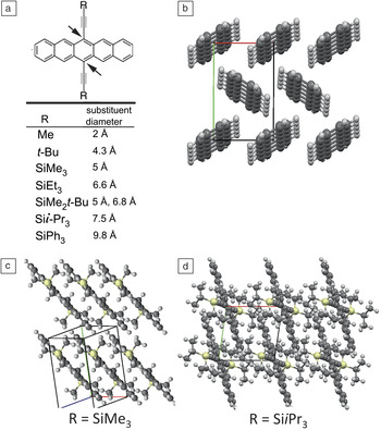
As an example, pentacene has a high hole transport mobility, and recent studies have demonstrated that single crystalline and highly pure pentacene crystals have mobilities as high as 35 cm2 V–1 s–1 at room temperature.Reference Klauk, Halik, Zschieschang, Schmid, Radlik and Weber43, Reference Jurchescu, Baas and Palstra44 Depending on the bulkiness of the 6 and 13 position (Figure 1a, arrows) substituents in pentacene, its resulting packing structure can be either a 1D slipped-stack packing motif, characterized by strong intermolecular interactions along one axis, or a 2D brick-wall packing motif, characterized by strong intermolecular interactions along two axesReference Anthony, Eaton and Parkin42, Reference Anthony, Brooks, Eaton and Parkin45, Reference Liu, Song, Zeng, Zhou, Shi, Ma, Yang, Zhang and Gong46 (Figure 1). These bulky substituent pentacene derivatives are stable and solution soluble.Reference Anthony, Eaton and Parkin42 The brick-wall packing structure may increase the intrinsic charge-transport properties because of good electronic overlap along the OSC π-conjugated backbones and a 2D film morphology.
Using chemical modifications to tune molecular packing. (a) Chemical structure of 6,13-substituted pentacene. The 6 and 13 positions (arrows) can be modified with a variety of substituents, R, such as those listed here. (b) The herringbone packing motif in a thin film of pentacene.Reference Yoshida and Sato47 (c) Single-crystal packing structure of R = SiMe3 pentacene derivative, showing 1D slipped-stack packing.Reference Anthony, Eaton and Parkin42 (d) Single-crystal structure of R = Sii Pr3 pentacene derivative, showing 2D brick-wall packing.Reference Mannsfeld, Tang and Bao48 In (b) and (d), the rectangle marks the view of the unit cell looking down from the c-axis, with the red and green lines representing the a- and b-axes. The atoms present in the organic semiconductors are represented as spheres (white = hydrogen, black = carbon, yellow = sulfur).

Several reviews have already discussed the chemical structure-molecular packing relationships for a variety of small molecule OSCs.Reference Takimiya, Shinamura, Osaka and Miyazaki41, Reference Tang, Oh, Reichardt and Bao49–Reference Anthony, Facchetti, Heeney, Marder and Zhan51 Briefly, Moon et al. have shown that chlorination of tetracene changes the molecular packing from a herringbone structure to a slipped-stack structure.Reference Moon, Zeis, Borkent, Besnard, Lovinger, Siegrist, Kloc and Bao52 Increasing the number of chlorination sites in a perylene-3,4:9,10-tetracarboxylic diimide backbone also changes the molecular packing from a herringbone arrangement to either a planar or a 2D contorted brick-wall packing.53
Additionally, Reese et al. have shown that attaching bulky trimethylsilane side groups to an aromatic oligothiophene core can significantly affect the tilt and packing compared to the unsubstituted oligothiophene core.Reference Reese, Roberts, Parkin and Bao54 The tilt of the molecular packing can cause improved electronic overlap between OSC molecules in a crystal, thus improving charge carrier mobility. The use of OSCs that can pack together stoichiometrically as a co-crystal can be used as an alternative route to modify molecular packing by making OSC dimers.Reference Sokolov55 Finally, Che et al. have incorporated hydrogen-bonding pyrazolyl and imidazolyl units into organoplatinum (II) complexes to reduce the π–π stacking distances and increase charge transport mobilities.Reference Che, Chow, Yuen, Roy, Lu, Chen, Chui and Zhu56 Chemical modifications are widely used to change the molecular packing of OSCs and subsequently affect charge transport properties in these materials.
Controlling packing through co-deposition
A second, but less frequently used, method to control molecular packing is through co-deposition of two similar OSCs that possess slightly different crystal packing structures. This method of tuning crystal lattice parameters is reminiscent of methods used in the inorganic semiconductor industry, where epitaxial deposition of silicon and germanium is used to strain the silicon lattice.Reference Thompson, Armstrong, Auth, Cea, Chau, Glass, Hoffman, Klaus, Ma, McIntyre, Murthy, Obradovic, Shifren, Sivakumar, Tyagi, Ghani, Mistry, Bohr and El-Mansy57 Unlike synthetic methods, this method usually only affords small changes to the OSC crystal structure. For example, the OSCs copper phthalocyanine (H16CuPc) and copper-hexadecafluoro-phthalocyanine (F16CuPc) have been co-deposited by Opitz et al., and the lattice spacing was found to be dependent on the H16CuPc concentration.Reference Opitz, Ecker, Wagner, Hinderhofer, Schreiber, Manara, Pflaum and Brutting58 The interlayer spacing linearly changed as a function of composition, from 1.3 nm for pure H16CuPc to 1.45 nm for pure F16CuPc. While the H16CuPc/F16CuPc bilayer has reciprocal lattice peaks similar to those of the pure phases, the co-deposited blend showed reciprocal lattice peaks between the two pure phases.Reference Opitz, Ecker, Wagner, Hinderhofer, Schreiber, Manara, Pflaum and Brutting58
Co-deposition has also been performed with pentacene and perfluoropentacene to tune the ionization energy of the resulting thin film.Reference Salzmann, Duhm, Heimel, Oehzelt, Kniprath, Johnson, Rabe and Koch59 Similarly, by varying the relative concentrations of α-sexithiophene (6T) or the alkylated version, α,ω-dihexylsexithiophene (DH6T), with the phenyl analogue sexiphenyl (6P), intercalation and subnanometer control of the lattice spacing was achieved.Reference Vogel, Salzmann, Opitz, Duhm, Nickel, Rabe and Koch60 These intercalated 6T/DH6T thin films were then used to tune the performance of organic transistors from enhancement to depletion modes.Reference Cosseddu, Vogel, Fraboni, Rabe, Koch and Bonfiglio61
More recently, Huang et al. have shown that two similar molecules, 2,5-bis(4-biphenylyl)-thieno[3,2-b]thiophene (BPTT) and 2,7-bis(4-biphenylyl)-phenanthrene (BPPh), can be co-deposited epitaxially to form an induction layer for another OSC, vanadyl phthalocyanine (VOPc). Tuning the lattice parameter of this induction layer varied the morphology of VOPc and the injection barrier. VOPc mobilities as high as 3.0 cm2 V–1 s–1 were obtained using this method.Reference Huang, Liu, Qiao, Tian, Geng and Yan62 The use of co-deposited OSCs finely tunes the crystal packing, but the degree of tuning is restricted to the range between the original packing structures of the pure OSCs.
Changing molecular packing through the use of an interfacial layer
Many polymorphs of the same OSC molecule can be present because of the weak intermolecular bonding in OSC crystals. One method of introducing polymorphism is to use the “symmetry breaking effect” of different interfaces to prevent crystal formation from equilibrium growth. In pentacene, at least four polymorphs are known and are characterized by their different interlayer d(001) spacings.Reference Mattheus, de Wijs, de Groot and Palstra63 Recently, Mannsfeld et al. showed that the first layer of pentacene on amorphous SiO2 grows in a herringbone fashion, with the pentacene molecules upright on the surface; this structure differs from other known pentacene polymorphs.Reference Mannsfeld, Virkar, Reese, Toney and Bao64 This interfacial structure has a higher electronic overlap compared to the other pentacene polymorphs, resulting in a higher mobility in pentacene thin films than the reported bulk single-crystal mobility.
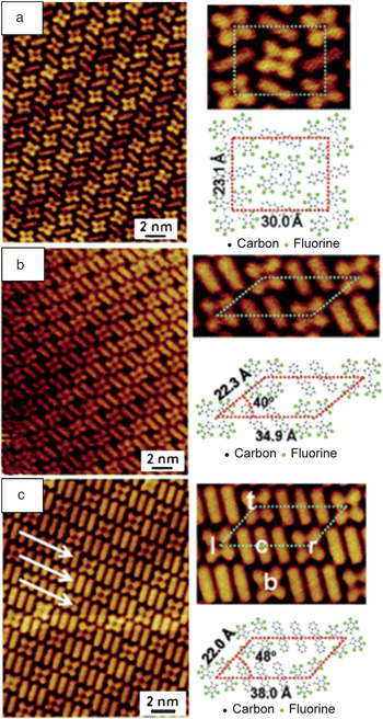
Another well-studied effect of changing molecular packing of OSCs is through the use of single crystalline metallic or graphitic interfaces. Single crystalline metal surfaces and the interface dipole moments formed between the metal and OSC molecules can be used as an ordering layer for OSCs. This effect has been studied for a variety of OSCs, such as C60, phthalocyanines, and porphyrins on different metal surfaces such as Cu(111), Ag(111), and Au(111).Reference Yoshimoto and Kobayashi65–Reference Chen, Pan, Yan, Wan, Matsuo and Nakamura68 Co-deposition of different adsorbates have also been studied, forming mono- and multilayers where the adsorbates pack as co-crystals.Reference Fendrich, Wagner, Stohr and Moller69–Reference Wei and Reutt-Robey72 Wakayama et al.Reference Wakayama, de Oteyza, Garcia-Lastra and Mowbray70 have deposited mixed F16CuPc:pentacene blends at different relative concentrations on Au(111). It was observed that phase segregation occurred at >50% F16CuPc. However, different crystalline phases and packing were observed at 3:1, 2:1, and 1:1 ratios of F16CuPc:pentacene (Figure 2).
Different packing structures in pentacene: F16CuPc blends with a ratio of (a) 1:1, (b) 2:1, and (c) 3:1. The lattice structure changes significantly.Reference Wakayama, de Oteyza, Garcia-Lastra and Mowbray70 For an increasing ratio, the crystal unit cell accommodates the increasing density of pentacene molecules. The molecules were assembled in rows (arrows) in a similar manner to pentacene assembly. Pentacene at the trimer center and surrounding four F16CuPc were labeled c, t, b, l, and r, respectively. Adapted from Reference Reference Wakayama, de Oteyza, Garcia-Lastra and Mowbray70 with permission. © 2011 American Chemical Society.

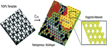
De Wild et al. observed the formation of a crystalline phase when co-depositing chloro[subphthalocyanianto] boron(III) (SubPc) and C60.Reference de Wild, Berner, Suzuki, Yanagi, Schlettwein, Ivan, Baratoff, Guentherodt and Jung71 Recently, Wei and Reutt-Robey have shown Kagome lattice packing of C70 molecules on a layer of titanyl phthalocyanine (TiOPc) (Figure 3), showing directed design of OSC molecular packing is possible, which can lead to higher mobilities.Reference Wei and Reutt-Robey72 Blunt et al. have also extended self-assembly into the third dimension. They deposited a layer of p-terphenyl-3,5,3,“5”-tetracarboxylic acid (TPTC) onto highly oriented pyrolytic graphite, and then deposited C60 as a guest molecule. The C60 molecules were deposited in the pores formed by the first layer of TPTC, after which a subsequent layer of TPTC was deposited above and parallel to the surface.Reference Blunt, Russell, Gimenez-Lopez, Taleb, Lin, Schroder, Champness and Beton73 Thus, molecular packing and crystallization can be modified in a variety of ways, such as using crystal-metal or crystal-graphite interfaces.
Kagome lattice of C70 on TiOPc.Reference Wei and Reutt-Robey72 Left: a TiOPc monolayer on a metal surface. Right: deposition of C70. Green signifies the TiOPc template layer, red signifies the first layer of deposited C70, and yellow signifies the second layer of C70 that deposits in a Kagome style lattice. Adapted from Reference Reference Wei and Reutt-Robey72 with permission. © 2011 American Chemical Society.

Tuning molecular packing through varying processing conditions
Controlling OSC polymorph formation and the crystal packing through processing conditions is also being actively explored. Cheng and Lin showed that solvent annealing of pentacene using p-xylene and other solvents changes the crystal structure from a metastable “thin-film” polymorph to a more stable “bulk” polymorph.Reference Cheng and Lin74
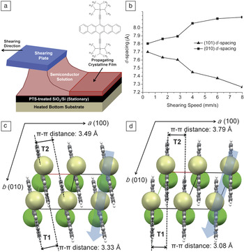
Solution shearing is another method that can be used to tune the crystal packing. In this method, an OSC solution is sandwiched in between a nonstick, moving blade and a heated device substrate. As the blade is translated, an evaporation front is created where the solvent evaporates and a uniform OSC thin film is cast on the device substrate. Giri et al. showed that by controlling the shearing speed, the molecular packing of 6,13-bis(triisopropyl-silylethynyl) pentacene (TIPS-pentacene) changes from the thermodynamically stable single-crystal structure to metastable crystal structures.Reference Giri, Verploegen, Mannsfeld, Atahan-Evrenk, Kim, Lee, Becerril, Aspuru-Guzik, Toney and Bao75 Because of the rapid solvent evaporation during solution shearing, metastable, “lattice strained” crystal packing structures are obtained (Figure 4). Interestingly, in the case of TIPS-pentacene, the lattice strained structure leads to a shorter π–π stacking distance, which is the distance between the π-conjugated faces of the OSC, leading to a higher charge-carrier mobility. This method is applicable to electronic device fabrication because it can be readily adapted for large-area deposition.
Tuning the crystal packing by solution shearing. (a) Schematic of 6,13-bis(triisopropyl-silylethynyl) pentacene (TIPS-pentacene) solution shearing on phenyl-trichlorosilane (PTS) treated silicon oxide/silicon substrates. (b) Lattice strain in TIPS-pentacene at different shearing speeds. (c) Thin-film molecular packing structure of evaporated TIPS-pentacene. (d) Thin-film molecular packing structure of solution sheared and lattice strained TIPS-pentacene. The green and yellow spheres indicate the TIPS side group. The blue arrow represents the fast charge transport direction. T1 and T2 denote the unique molecular pairs. Adapted from Reference Reference Giri, Verploegen, Mannsfeld, Atahan-Evrenk, Kim, Lee, Becerril, Aspuru-Guzik, Toney and Bao75 with permission. © 2011 Nature Publishing Group.

The control of molecular crystal packing is an exciting area of research in the OSC community because of its potential to achieve higher device charge-carrier mobilities. The control of organic small molecule polymorphs has also been extensively explored in the pharmaceutical industry.Reference Bag, Patni and Reddy76, Reference Lopez-Mejias, Knight, Brooks and Matzger77 Bag et al.Reference Bag, Patni and Reddy76 have demonstrated the concept of growing metastable polymorphs using kinetically controlled conditions (through rapid solvent evaporation). Also, different polymorphs can be selected using nano-confinement, as well as directed epitaxial growth on molecular crystal substrates.Reference Beiner, Rengarajan, Pankaj, Enke and Steinhart78, Reference Mitchell, Yu and Ward79 These methods may also be useful to create OSC polymorphs and to explore the metastable states that improve charge transport.
Large-area fabrication of single-crystal FETs
Organic single crystals with long-range periodic molecular packing are desired for FETs, as the intrinsic charge transport properties are not degraded because of the absence of grain boundaries. Approaches for fabricating single-crystal transistors are widely studied and have been previously reviewed.Reference Reese and Bao23, Reference Li, Hu, Liu and Zhu80 Here, we focus on single-crystal growth methods that are potentially applicable for large-area fabrication for arrays of devices and thus are promising for technological applications. Although chemists have investigated the growth mechanisms in organic crystals, nonetheless the coupling of crystal growth and device fabrication is still challenging, especially for large-area devices (a criterion desired for most organic electronic products). Typically, integrating device arrays on substrates requires growth of single crystals over a large area, as well as precise positional control between the crystals and electrodes. This section surveys two aspects, namely patterning and aligning single crystals, to achieve this aim.
Patterning single crystals
Patterning of OSCs achieves large arrays in devices.Reference Menard, Meitl, Sun, Park, Shir, Nam, Jeon and Rogers81 Patterning precisely controls the position between semiconductors and electrodes and also minimizes cross-talk between adjacent devices. Typically, OSCs do not grow into large single crystals (e.g., smaller than millimeter-scale), and the fabrication of large arrays of single-crystal FETs relies on bottom-up patterning techniques.
Patterning nucleation sites
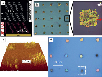
OSC crystal patterning has been achieved on substrates modified by self-assembled monolayers (SAMs).Reference Briseno, Aizenberg, Han, Penkala, Moon, Lovinger, Kloc and Bao82 Briseno et al. examined the growth of anthracene crystals on SAM-modified gold-coated substrates. They found that crystals nucleated from oligophenylene thiol SAMs in an epitaxial fashion, and the selective nucleation is associated with the interaction between the terminal group of SAMs and the OSC (Figures 5a–b). Oligophenylene-thiols were favored for OSC nucleation rather than alkanethiols. When SAMs with different nucleation activities were micropatterned, crystals were selectively nucleated and formed patterns as governed by the SAMs (Figure 5b).
Patterning nucleation sites. (a) Molecular modeling of (001)-oriented anthracene crystals on a terphenylthiol (-3P) self-assembled monolayer (SAM). (b) Optical micrographs of the patterned anthracene crystals. Crystal nucleation occurs from the -3P SAM regions (red arrow) and not from the HS(CH2)11CH3 SAM regions (white arrow). The patterned domains are 100 × 100 μm2. (c) A 3D atomic force microscopy image (20 × 20 μm2) of an OTS layer with polydimethylsiloxane regions (5 × 5 μm2) on a SiO2 substrate. (d) An optical micrograph of patterned C60 single-crystal arrays. The white dashed square indicates the size and location of one of the octadecyltriethoxysilane-stamped domains. Adapted from References Reference Briseno, Aizenberg, Han, Penkala, Moon, Lovinger, Kloc and Bao82 (© 2005 American Chemical Society) and 83 (© 2006 Nature Publishing Group) with permission.

In addition to SAMs, Briseno et al. used rough surfaces as nucleation sites to pattern crystals. They successfully fabricated large FET arrays based on the patterned single crystals.Reference Briseno, Mannsfeld, Ling, Liu, Tseng, Reese, Roberts, Yang, Wudl and Bao83, Reference Mannsfeld, Briseno, Liu, Reese, Roberts and Bao84 Octadecyltriethoxysilane (OTS, average thickness 13 ± 2 nm) films were micropatterned onto SiO2/Si surfaces using a polydimethylsiloxane (PDMS) stamp (Figure 5c). Crystals selectively nucleated from the rough OTS-coated regions (Figure 5d). Both p- and n-type crystal patterns, including rubrene, pentacene, tetracene, C60, fluorinated copper phthalocyanine (F16CuPc), and tetracyanoquinodimethane (TCNQ) were demonstrated. Since the OTS-coated domain is small enough to support only one nucleation event, patterning of discrete single crystals was achieved, and device arrays based on individual single crystals became possible (Figure 5d).
Besides OTS-coated surfaces, Liu et al. used spray-coated carbon nanotube (CNT) bundles to introduce rough surfaces as nucleation sites to obtain patterned OSC crystals.Reference Liu, Briseno, Mannsfeld, You, Locklin, Lee, Xia and Bao85 They also used an Au film with defined hole patterns (Au mask), to directly pattern α-sexithiophene single crystals that nucleated from the rough edges of the holes.Reference Liu, Mannsfeld, Wang, Sun, Stoltenberg and Bao86 One of the advantages of this method is that both the size and shape of the crystals are dictated by the holes in the mask, hence facilitating device fabrication.
In all the methods presented, patterning of OSC single crystals is achieved via nucleation sites. In the OTS/CNT-nucleation method, the crystals nucleate from rough surfaces; therefore the semiconductor/dielectric interfaces are also rough,Reference Mannsfeld, Briseno, Liu, Reese, Roberts and Bao84, Reference Liu, Briseno, Mannsfeld, You, Locklin, Lee, Xia and Bao85 and the orientation and alignment of the crystals are thus random. These features reduce device performance. In contrast, SAM surfaces are smooth, and epitaxial crystal growth is achieved. Crystals grown from SAMs usually exhibit smooth interfaces and controlled crystallographic orientation and alignment. However, it is not possible to pattern only one single crystal in a defined orientation, as the nucleation density is too high.
Patterning solution/dispersion droplets
As OSCs are usually soluble in organic solvents, solution deposition methods, which are cost-effective compared to vacuum deposition methods,Reference Laudise, Kloc, Simpkins and Siegrist87 can be used to grow the crystals. Another advantage of solution deposition is that the “precursor” OSC crystal solutions can be easily patterned, hence providing a facile approach to the patterning of solution-grown crystals. In addition to solutions, OSC dispersions in solvents can serve as crystal carriers for patterning.
The wetting/dewetting method was first used to pattern OSC solutions. Liu et al. patterned OSC crystals on substrates with patterned wettability.Reference Liu, Wang, Mannsfeld, Locklin, Erk, Gomez, Richter and Bao88 Depending on the different solvent–substrate interactions, OSC crystals dispersed in solvents can be selectively deposited or removed, resulting in desired patterns. Mannsfeld et al. developed a simple and efficient method to pattern organic single-crystal FETs from solutions.Reference Mannsfeld, Sharei, Liu, Roberts, McCulloch, Heeney and Bao89 A solution of OSCs was first dispersed into tiny droplets in a water host where a liquid vortex was created by rapid stirring before being poured onto a FET substrate pre-patterned with gold pad electrodes. Since the OSC organic solution has better wettability on the gold pads compared to the OTS-modified SiO2 surface, a clean pattern of droplets is achieved. The droplets evaporate, and single crystals are formed. Although the researchers have patterned only two OSCs [bis(cyclohexyl)-α-quaterthiophene and trimethylsilane-aquarterthiophene],Reference Mannsfeld, Sharei, Liu, Roberts, McCulloch, Heeney and Bao89 this method should be applicable to pattern other OSCs as well, as only the wetting characteristics of the solution is important.
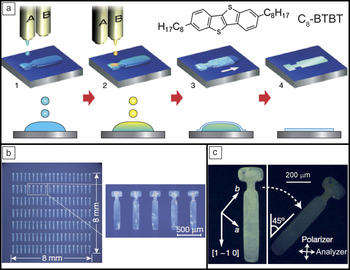
One advantage of this method is that OSC crystals adhere easily to the gold electrodes, which facilitates device fabrication. In addition to forming droplets using the liquid vortex technique, micro-liquid inkjet printing techniques are also being used to print droplets directly onto a substrate with pre-patterned wetting/dewetting regions (Figure 6).Reference Minemawari, Yamada, Matsui, Tsutsumi, Haas, Chiba, Kumai and Hasegawa24 Subsequent crystallization from the droplet solutions results in patterned single crystals. Using this method, single-crystal arrays of 2,7-dioctyl[1]benzothieno[3,2-b][1] benzothiophene (C8-BTBT) were prepared. The observed maximum hole mobility was 31.3 cm2 V–1 s–1 (average over 54 FETs: 16.4 ± 6.1 cm2 V–1 s–1), which is one of the highest reported values for OSCs and the highest value reported for solution-processed OSCs.
(a) Schematic of the inject printing process for organic semiconductor (OSC) crystals. Antisolvent ink is inkjet-printed (step 1), and then OSC solution ink is dropped on top to form intermixed droplets confined to a predefined area (step 2). OSC crystals nucleate at the liquid-air interface (step 3), before the solvents completely evaporate (step 4). (b) Micrographs of a 20 × 7 array of inkjet-printed C8-BTBT single crystal. (c) Crossed Nicols polarized micrographs of a crystal with the entire crystal extinguishing the light simultaneously, thus showing single crystallinity. Adapted from Reference Reference Minemawari, Yamada, Matsui, Tsutsumi, Haas, Chiba, Kumai and Hasegawa24 with permission. © 2011 Nature Publishing Group. Note: (C8-BTBT), 2,7-dioctyl[1]benzothieno[3,2-b][1] benzothiophene.

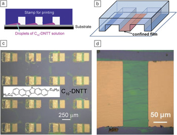
Recently, NakayamaReference Nakayama, Hirose, Soeda, Yoshizumi, Uemura, Uno, Li, Kang, Yamagishi, Okada, Miyazaki, Nakazawa, Nakao, Takimiya and Takeya19 and Akkerman et al.Reference Akkerman, Li and Bao90 reported another interesting approach to pattern OSC solutions by spatially confining the solution droplets using a template (Figure 7). This method is similar to conventional micro-contact printing processes,Reference Qin, Xia and Whitesides91 except that an inclined gap (Figure 7a) or a restricted channel (Figure 7b) confines the solution volume, allowing the solution to crystallize onto defined regions. Using this method, 2,9-alkyl-dinaphtho[2,3-b:2,‘3’-f]thieno[3,2-b]thiophene (C10-DNTT) single crystals were successfully patterned on both rigid (SiO2/Si) and flexible polyethylene naphthalate substrates. FETs based on the patterned crystals exhibit hole mobilities as high as 11 cm2 V–1 s–1 (average over 16 FETs: 7 cm2 V–1 s–1).
(a–b) Schematic of the organic semiconductor (OSC) solution patterning droplet process. A stamp is designed with gaps (a) or channels (b) to confine droplets of OSC solution. (c–d) Micrographs of a 4 × 4 array of OSC crystals (green) patterned using the stamp. Adapted from References Reference Nakayama, Hirose, Soeda, Yoshizumi, Uemura, Uno, Li, Kang, Yamagishi, Okada, Miyazaki, Nakazawa, Nakao, Takimiya and Takeya19 (© 2011 Wiley) and 90 (© 2012 Elsevier) with permission. Note: C10-DNTT, 2,9-alkyl-dinaphtho[2,3-b:2,‘3’-f]thieno[3,2-b]thiophene.

Patterning techniques using OSC solution droplets confines the area on which the OSC crystals can grow, leading to the patterning of crystals. To obtain single crystals, the crystallization process inside the droplets (especially the nucleation event) should be controlled. For example, Minemawari et al. showed that the protuberant shape of the droplets seen in Figure 6a is necessary for controlled nucleation of crystals and to avoid polycrystal formation.Reference Minemawari, Yamada, Matsui, Tsutsumi, Haas, Chiba, Kumai and Hasegawa24
Pattern etching a big piece of crystal
OSCs seldom form large flat single crystals, but when they do, top-down techniques can be used for patterning.Reference Siegrist, Kloc, Laudise, Katz and Haddon92–Reference Briseno, Tseng, Ling, Falcao, Yang, Wudl and Bao95 Bae et al. developed a method called selective contact evaporation printing to selectively etch a cm-sized TIPS-pentaceneReference Anthony, Brooks, Eaton and Parkin45 single crystal to produce patterned micron-sized single crystals.Reference Bae, Kang, Shin, Park, Kim, Mathevet and Park94 During the process, a PDMS mold in contact with a heated TIPS-pentacene single crystal results in pseudo adiabatic conditions for effective heat accumulation, which evaporates the TIPS-pentacene. Recently, a similar method was used to pattern rubrene crystals.Reference Lee, Kim, Choi and Cho96
Aligning single crystals
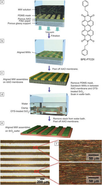
Current flows unidirectionally in an FET, while charge-carrier transport is anisotropic in most OSC single crystals.Reference Sundar, Zaumseil, Podzorov, Menard, Willett, Someya, Gershenson and Rogers16, Reference Li, Jiang, Meng, Gao, Li, Tang, He, Hu, Liu and Zhu97–Reference He, Zhang, Jia, Li and Tao99 Hence, to achieve maximum performance, organic single crystals need to be aligned to allow current to flow along the direction of the highest mobility. Alignment facilitates the relative position between crystals and electrodes, as the source and drain electrodes can be easily deposited perpendicular to the alignment direction. Oh et al. described a filtration and transfer method to align OSC single crystals (Figure 8).Reference Oh, Lee, Mannsfeld, Stoltenberg, Jung, Jin, Kim, Yoo and Bao15 A dispersion containing single-crystalline microwires (MW) of N,N’-bis(2-phenylethyl)-perylene-3,4:9,10-tetracarboxylic diimide (BPE-PTCDI) was prepared. The suspension was filtered in vacuo through a PDMS template with channels where the MWs could be aligned by fluid flow. The degree of alignment was observed to be associated with the vacuum pressure and the MW length, with lower pressure and longer MW length leading to a better alignment. The aligned MWs were finally transferred onto FET substrates to complete the device fabrication. Although the alignment was demonstrated on a substrate of 2.5 cm in diameter, a larger operational area should also be achievable.
(a–e) Schematic illustration of the filtration and transfer process. (a) A microwire (MW) dispersion is filtered by vacuum through a polydimethylsiloxane (PDMS) mask placed on a porous anodized aluminum oxide (AAO) membrane. (b) After vacuum filtration, MWs are aligned along PDMS mask channels. (c) Removal of the AAO membrane. (d) Transfer of the MWs onto field-effect transistor substrates (SiO2/Si wafer covered by n-octadecyl triethoxysilane [OTS]). (e) Removal of the AAO and PDMS masks and transfer of the MWs onto the wafer. (f) Micrographs of the obtained aligned MWs. Adapted from Reference Reference Oh, Lee, Mannsfeld, Stoltenberg, Jung, Jin, Kim, Yoo and Bao15 with permission. © 2009 National Academy of Sciences. Note: BPE-PTCDI, N,N’-bis(2-phenylethyl)-perylene-3,4:9,10-tetracarboxylic diimide.

In addition to the filtration and transfer method (in which the crystals are first grown and then aligned), both the growth and alignment processes can be coupled together in one simple step. Dip coating,Reference Rogowski, Dzwilewski, Kemerink and Darhuber100, Reference Li, Gao, Schuermann, Ostendorp, Wang, Du, Lei, Fuchs, De Cola, Mullen and Chi101 solution-shearing deposition,Reference Becerril, Roberts, Liu, Locklin and Bao102, Reference Liu, Becerril, Roberts, Nishi and Bao103 zone casting,Reference Pisula, Menon, Stepputat, Lieberwirth, Kolb, Tracz, Sirringhaus, Pakula and Mullen104–Reference Duffy, Andreasen, Breiby, Nielsen, Ando, Minakata and Sirringhaus106 and confined solution depositionReference Akkerman, Li and Bao90 were used to grow aligned OSC crystals from solution. The directional receding of the solution meniscus leads to crystal alignment. It is only when the growth conditions are well-controlled that aligning single crystals becomes possible. For example, the droplet-pinned methodReference Li, Tee, Cha, Cui, Chung, Lee and Bao31, Reference Uemura, Hirose, Uno, Takimiya and Takeya107–Reference Li, Tee, Giri, Chung, Lee and Bao109 was developed recently to provide a steady condition for crystal growth, and aligned single crystals of C60, and TIPS-pentacene have been obtained.
Conclusions
Tuning molecular packing of organic semiconductors (OSCs) is an effective method to control charge transport characteristics. Chemical modifications on well-known high-performance OSC systems such as acenesReference Anthony, Eaton and Parkin42 and thienoacenesReference Oh, Suraru, Lee, Konemann, Hoffken, Roger, Schmidt, Chung, Chen, Wurthner and Bao38 have successfully improved their charge transport properties and device performance.Reference Wang, Dong, Hu, Liu and Zhu110 Preparation of metastable polymorphs with shorter π–π stacking distances and selective displacement allows further tuning. To make use of OFETs in electronic applications with their highest (intrinsic) performance, large-area fabrication of OSC single crystals is desired. We believe that progress will be made to achieve this goal by patterning or aligning OSC single crystals. Simultaneous control of both single-crystal patterning and alignment will further increase FET performance. Practical electronic applications of single-crystalline high-performance OFETs require integrated materials engineering with both preferential microscopic molecular packing as well as large-scale oriented crystalline domains. As such, this is one of the most challenging issues, and future efforts need to be directed toward developing materials with both high intrinsic charge transport properties and facile processability to prepare large-scale single crystals.
Acknowledgments
This work was supported by the National Science Foundation (NSF) Division of Materials Research (DMR) Solid-State Chemistry under Award DMR-0705687–002, Air Force Office of Scientific Research (AFOSR) (Grant No. FA9550–12–1-01906) and the Stanford Global Energy and Climate Program. This work was partially supported by the National Natural Science Foundation of China (Grants No. 51222302) the Fundamental Research Funds for the Central Universities (2012 QNA 4025), and the Department of Energy, Laboratory Directed Research and Development funding, under contract DE-AC02-76SF00515.