I. INTRODUCTION
Ultra-wideband (UWB) is fast growing technology, which makes use of unlicensed frequency band (3.1–10.6 GHz) allocated by US-FCC, to transmit signals at higher data rates. This frequency band can be used to setup personal networks to control different devices within home or office [1]. As with any wireless communication there is an effect of multipath fading which degrades the system performance. Multiple-input multiple-output (MIMO) is a technique that can be employed to reduce the effects of fading and hence increase the system performance [Reference Foschini and Gans2]. Using multiple antennas at transmitter and receiver, data rate of the system can also be increased. Performance of MIMO system depends upon the isolation between the antenna elements, it is however difficult to increase the isolation between antennas on the limited space available.
Besides there are various narrowband communication systems such as WiMAX (3.4–3.6 GHz) and WLAN (5.725–5.825 GHz) working in UWB, and in order to cancel the interference between UWB and these narrowband systems, antennas should have band-notched characteristics [Reference Sung3].
So far various MIMO antennas have been reported to achieve wideband isolation over entire UWB using different decoupling methods to obtain isolation [Reference Zhang, Ying, Xiong and He4–Reference Gao, He, Wei, Xu, Wang and Zheng8]. Decoupling has been achieved by a tree-like structure in the ground plane [Reference Hallbjörner9], by stubs [Reference Chen, Yang, Guo and Chia10] and by etching slots in the ground to reduce coupling between radiators [Reference Gogosh, FarhanShafique, Saleem, Usman and Faiz5]. However, in the UWB MIMO antennas [Reference Zhang, Ying, Xiong and He4–Reference Gao, He, Wei, Xu, Wang and Zheng8, Reference Liu, Wang, Yin, Ren and Wu11–Reference Liu, Cheung and Yuk13] band-rejected characteristics are not employed and hence these cannot be used in environments with WiMAX and WLAN.
Though there have been reports on antennas with band rejected characteristics [Reference Lee, Kim, Ryu and Woo14–Reference Gao, He, Wei, Xu, Wang and Zheng17], yet in [Reference Lee, Kim, Ryu and Woo14] an UWB MIMO antenna is proposed with single band-notch characteristics using λ/2 open stub. This stub will be large if WiMAX band is to be rejected using the same antenna. In [Reference He15] a polarization diversity antenna is proposed for UWB MIMO application with triple band-notched characteristics. This antenna has an overall size of 60 × 30 = 1800 mm2. Dual-band-notched UWB MIMO antenna is presented in [Reference Tang and Lin16], wherein band-notch and decoupling (|S12| > 15 dB) is achieved using neutralization lines, with dimensions 40 × 30 = 1200 mm2.
In this paper, a compact dual-band-notched UWB antenna is proposed for MIMO application. Our proposed antenna has size of 35 × 30 = 1050 mm2 about 42 and 12% smaller than those in [Reference He15, Reference Tang and Lin16], respectively. It consists of two monopoles separated by ground stub and slots to achieve maximum isolation. Notched characteristics are achieved using complementary split ring resonator (SRR) etched in the radiators. Antenna system covers entire UWB with notched bands 3.4–3.6 GHz (WiMAX) and 5.725–5.825 GHz (WLAN), thus is an ideal candidate to avoid interference in these bands. Moreover, this antenna achieves an isolation of 20 dB in most of the band with envelope correlation coefficient (ECC) value less than 0.015.
II. ANTENNA SYSTEM AND ANALYSIS
A) Antenna configuration
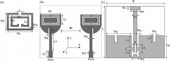
The proposed antenna system shown in Fig. 1 consists of two identical elements placed in mirror configuration about Y-axis on Roger 5870 substrate with volume 35 × 30 × 0.8 mm3.
Antenna configuration. (a) CSRR, (b) front side, and (c) back side.

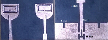
Antenna system consists of two identical cup-shaped monopole radiators to achieve UWB characteristics. They share common ground with rectangular slots and a ground stub to achieve better isolation. Both antennas are fed with 50 Ω microstrip lines spaced by distance, ds (=0.3 λg/2 at 3 GHz) from each other. The antenna system has been optimized using CST Microwave Studio, the optimized dimensions of the fabricated prototype is as follows (millimeters): W = 35, L = 30, Lg = 13, Wa = 10, Wb = 5.5, Wm = 0.4, W1 = 8.4, W2 = 3.9, g = 0.5, Lj = 0.4, We = 1.5, Wf = 2.4, Le = 9.8, Lf = 4, Wn = 1.5, Ln = 4, Lk = 3, Wk = 0.5, L1 = 7, Wp = 1.2, Lh = 5, Lu = 4, Wt = 6, r = 6, Wr = 12, Lr = 5.5, th = 1, Wh = 4.4, S = 1.5. The effect of these dimensions and effectiveness of slots and stubs are presented below. The fabricated prototype antenna is shown in Fig. 2.
Photograph of prototype antenna.

B) Ground stub and rectangular slots
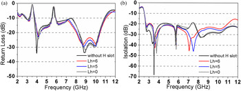
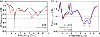
The rectangular slots in both the radiators next to feed lines are etched out in order to achieve impedance matching. For further matching of impedance two rectangular slots are made in the ground plane under the feed lines as shown in Fig. 2. A novel H-shaped slot is also cut in the ground plane between two radiators to improve return loss and isolation at around 7.3 GHz. By introducing H-slot, the return loss improves from 9.9 to 13 dB and isolation is increased to 23 dB at 7.3 GHz as observed in Fig. 3.
Effect of H-slot and length Lh on (a) |S11| and (b) |S12|.

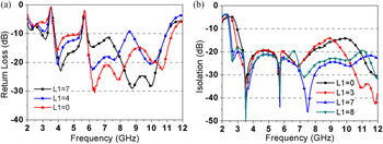
A novel T-shaped ground stub separating two radiators is added to achieve better isolation. This stub acts as monopole and resonates at frequency defined by its length. In order to increase the length of the T-stub so that it may reflect the lower frequencies between ports 1 and 2, this is done by etching the slots next to the stub in the ground plane. In this way we can achieve a good isolation at lower frequencies without any increase in the overall antenna size. This is an effective way to maintain the good isolation at this compact size. As shown in Fig. 2, the length of the T-stub is controlled by the length L1. It can be seen from Fig. 4(a) that with L1 = 0, lower cut-off frequency of the antenna is 4 GHz. With the increase in length L1 the return loss of antenna reduces at about 3 GHz. Another effect of increasing length L1 is, as the length of stub is increased isolation at lower frequencies (around 3 GHz) also increases. This could be due to the fact that the stub acts as a monopole and the distribution of surface current taking place around the stub gives rise to increased isolation. By etching slot1, two edges are formed in the ground plane. One edge controls the length of ground stub and the other acts as monopole increasing the isolation at higher frequency around 7.5 GHz as seen in Fig. 4.
Effect of variations in length L1 on (a) |S11| and (b) |S21|.

C) CSRR slot
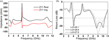
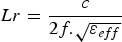
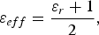
Figure 5(a) shows the S-parameters of the antenna without complementary split ring resonator (CSRR) slot. The notched characteristics at the desired frequencies 3.3 and 5.8 GHz are introduced by two complementary SRR slots etched in the radiators. As seen from the input impedance, in Fig. 6(a), antenna acts as short and open at notch frequencies 3.3 and 5.8 GHz, respectively. The outer split ring slot in CSRR act like two parallel open guided quarter wavelength transmission line to short the antenna at the desired frequency [Reference Kerkhoff and Ling18] and the inner ring working is analogous to two parallel shorted quarter wavelength transmission line, because outer and inner split rings are complementary to each other. The total length of the slot is chosen to be λ/2 at the designated frequency and can be calculated by
 $$Lr = \displaystyle{c \over {2f.\sqrt {{\varepsilon _{eff}}}}} $$
 $${\varepsilon _{eff}} = \displaystyle{{{\varepsilon _r} + 1} \over 2},$$
(a) Antenna S-parameters without CSRR. (b) Effect of variation in CSRR length Lr on |S11|.

(a) Input impedance plot. (b) Effect of variation in CSRR length Lr2 on return loss.

where ‘c’ is the speed of light, ε eff is the effective dielectric constant and Lr (Lr = 2(w1 + w2 + Lj) − g − 5 × Wm) is the average length of the SRR slot. According to (1), the length corresponding to 5.8 GHz comes out to be 20.04 mm.
Figure 5(b) shows the return loss at three different values of Lr = 20, 22.8, and 23 mm. It may be seen from the figure that, by increasing the length of SRR, the notched band moves to lower frequencies. In order to reject the center frequency 5.8 GHz the practical length of slot is found 22.8 mm.
Similarly, the average length of the outer SRR slot, Lr2 (Lr2 = 2(wa + wb) − g − 4 × Wm) controls the notched frequency band around 3.3 GHz. Figure 6(b) shows the effect of varying the length Lr2 on the return loss. The practical length of the slot for band notching at 3.3 GHz is found to be 28.9 mm.
III. RESULTS AND DISCUSSION
A) Impedance performance
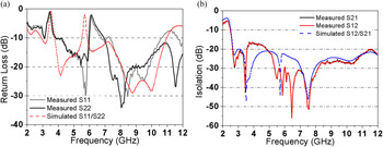
The antenna is designed using CST MWS and a prototype is fabricated with the optimized dimensions as above. The return loss of the antenna system is plotted in Fig. 7(a). It could be seen that the system covers the entire band with notched characteristics at 3.3 and 5.8 GHz. The isolation between the two radiators is shown in Fig. 7(b), the measured isolation is greater than 20 dB in the entire band. In the measured results as in Fig. 7(a), there is a shift in the upper notch frequency to 6 GHz. The increased width (Wm) in the fabricated prototype, which affects the average length (Lr) is the reason why the notch has shifted to higher frequency. Other discrepancies between the simulated and measured results might be due to the fact one the antenna system has been fabricated using chemical etching process and second the antenna ground plane is smaller in comparison with connectors [Reference Chen, Yang, Guo and Chia10].
Measured and simulated S-parameters of dual-element dual-notched antenna system. (a) Return loss. (b) Isolation.

B) Radiation performance
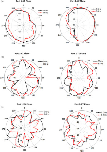
The radiation patterns of the prototype antenna are shown in Fig. 8 when it is excited at port1 and port2 at 5 and 8 GHz, respectively. As it can be seen the radiations patterns in the XY-plane are different when excited at port1 and port2 owing to pattern diversity, while as the patterns in the YZ-plane are mirror transformation of each other. The radiation patterns are stable in the entire UWB.
Measured radiation pattern of the dual-notch proposed antenna at 5 and 8 GHz. (a) XZ-plane, (b) YZ-plane, and (c) XY-plane.

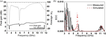
The simulated efficiency and gain of the antenna are plotted in Fig. 9(a). Evidently the antenna radiates efficiently with a stable gain in the entire UWB.
(a) Simulated efficiency and gain plot. (b) Measured and simulated ECC of the antenna.

C) Diversity performance
Diversity is use of multiple numbers of antennas at transmitter and receiver end to increase the number of possibilities for reception of low fade signals. This performance is measured in terms of ECC and is given below [Reference Hallbjörner9]:
 $$ECC = \displaystyle{{{{\left \vert {S_{11}^{\ast} S12 + S_{21}^{\ast} S22} \right \vert} ^2}} \over {(1 - ( \vert S11{ \vert ^2} + \vert S21{ \vert ^2}))(1 - ( \vert S22{ \vert ^2} + \vert S12{ \vert ^2}))}}.$$
Measured and simulated results show that the ECC is below 0.015 in the entire UWB as shown in Fig. 9(b), thus the proposed antenna is a potential candidate for diversity applications.
IV. CONCLUSION
Compact antenna with notched characteristics is proposed for application in the UWB MIMO system. This antenna consists of two monopole radiators formed on a low loss substrate of size 35 × 30 = 1050 mm2 to achieve UWB characteristics. Isolation between the antennas is obtained using ground stub and slots. To achieve notched characteristics CSRR is etched in both the radiators. Result show good performance in terms of impedance matching, as well as the isolation and stable radiation pattern. ECC below 0.015 is obtained proving this antenna to be a good candidate for UWB MIMO applications.
 Zamir Ah. Wani received his M.Sc. degree in Electronic Science from the University of Kashmir, India in 2011 and received his M.Tech. degree in Electronics and Communication Engineering from Indian Institute of Information Technology, Design and Manufacturing, Jabalpur, India in 2015. His main research interests include design of planar antennas for MIMO terminals, microwave circuits, and computational electromagnetics.
 Dr. Dinesh Kumar Vishwakarma received his Ph.D. degree in Electrical Communication Engineering from Indian Institute of Science, Bangalore in 2005. He is currently an Associate Professor with Department of Electronics and Communication Engineering, Indian Institute of Information Technology, Design and Manufacturing, Jabalpur, India. During 2006–2009, he was a visiting foreign researcher in Japan. Prior to this, he was employed in Ministry of Communication & IT through Indian Engineering Services. His research interests include computational electromagnetics, microwave circuits, antenna and wave propagation, photonics, and optical communication.