


Introduction
The ternary alloy InGaN has a direct band gap ranging from 1.9 eV (InN) to 3.4 eV (GaN) and has now shown its potentiality for light emitters in the visible range of the electromagnetic spectrum. [Reference Nakamura and Fasol1]. Most of the nitride based structures and devices are currently fabricated using metal-organic chemical vapor deposition (MOCVD), which has proven its ability for the growth of high quality nitrides [Reference Nakamura and Fasol1]. MBE is however emerging as an alternative growth technique. It allows the use of high efficiency in situ characterization tools (reflection high energy electron diffraction (RHEED), mass spectroscopy…) and high quality GaN can be grown in the two versions of the MBE of nitrides, i.e. using NH3 or an N2 plasma source [Reference Popovici, Morkoç, Mohammad and Gil2,Reference Grandjean, Massies, Vennéguès, Leroux, Demangeot, Renucci and Frandon3]. Presently, apart MOCVD, InGaN/GaN QW based LEDs have been reported only by plasma-assisted MBE growth [Reference Tews, Averbeck, Graber and Riechert4]. We show in this paper that NH3 is also well suited for achieving InGaN/GaN QWs with sharp interfaces. LEDs have been processed from that material and exhibit room temperature EL at 440 nm.
Experiments
The growth of GaN and InGaN was carried out in a Riber 32 P MBE system equipped with RHEED and laser reflectivity facilities. Ga and In were provided by double-filament effusion cells. A flow of 50 sccm of purified NH3 was used for the growth of both GaN and InGaN. Before growing the InGaN alloys or QW structures, 2 μm-thick GaN epilayer were deposited on (0001) sapphire substrates following the procedure described in ref. [Reference Grandjean, Massies, Vennéguès, Leroux, Demangeot, Renucci and Frandon3]. The substrate temperature was decreased around 600°C to grow InGaN. The growth rate is 0.2 μm/h and the thicknesses ranging from 70 to 200 nm. Concerning the In composition, it has been checked by XRD, Rutherford back scattering, and RHEED intensity oscillations. The two first techniques give roughly the same In composition while RHEED leads to larger values. Actually, RHEED intensity oscillations are observed only at the beginning of the growth. Therefore, a growth transient which can be provoked in particular by In surface segregation could affect the measurements. The structural properties of the layers were assessed by TEM and XRD. The optical properties were studied by PL using a 10 mW HeCd laser as excitation source.
Results and Discussions
The specificity of InGaN MBE growth with NH3, compared to plasma sources, is the cracking of this nitrogen precursor on the growing surface which depends on the substrate temperature. This implies that the amount of nitrogen active species is a function of the substrate temperature. For instance, it has been reported that the decomposition of NH3 below 450°C is insignificant [Reference Mesrine, Grandjean and Massies5]. When increasing the substrate temperature, the NH3 efficiency increases too but remains rather low (4 % at 700°C). Therefore, with the aim of growing GaInN alloy, we have to take care of the high dissociation rate of InN, the high In volatility and the NH3 cracking efficiency pattern. We have determined that the best InGaN properties are obtained for temperatures ranging between 570 and 620°C.
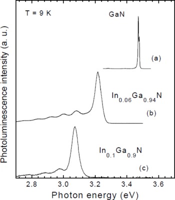
Fig. 1 displays two low temperature (9 K) PL spectra of InGaN layers grown at ∼600°C with a growth rate of 0.2 μm/h (the GaN spectrum is given in Fig. 1(a) as reference). The indium compositions are 6% and 10% in Figs. 1(b) and 1(c), respectively. A sharp PL peak (full width at half maximum (FWHM) of ∼50 meV) is observed for the two In compositions. The transition energies are 3.22 eV and 3.07 eV. The PL spectra of InGaN layers exhibits also deep luminescence on the low energy side of the main PL peak. Unfortunately, interference makes difficult to ascribe this luminescence to standard shallow donor acceptor pair recombinations or to deep-levels, or other origins (In rich and/or strain relaxed areas). When growth conditions depart from an optimum window, this deep-level PL dominates the spectra. Fig. 2 shows a cross section TEM image of a thin In0.06Ga0.94N layer (160nm) deposited at 570°C and 0.18 μm/h on GaN template. One can see that no further defects are introduced in the InGaN layer. Only the preexistent dislocations propagate into the InGaN layer resulting in pits at the surface as for the case of MOCVD growth [Reference Kawaguchi, Shimizu, Yamaguchi, Hiramatsu, Sawaki, Taki, Tsuda, Kuwano, Oki, Zheleva and Davis6].
9 K PL spectra of InGaN layers
TEM image in cross section of an In0.6Ga0.94N layer grown at 570°C and 0.18 μm/h

The strain state of the In0.06Ga0.94N layer has been checked by XRD reciprocal space mapping of the [-105] and [105] reflections. Fig. 3 shows that the 160nm-thick InGaN layer is almost perfectly pseudomorphically strained onto the GaN template.
reciprocal space mapping of the In0.06Ga0.94N layer grown on a GaN template

The InGaN alloys, previously characterized, have been used to grow InGaN/GaN QWs. Fig. 4 displays the 9 K PL spectrum of 3 GaInN/GaN QWs of width 25 Å. The In composition is about 10 %. For comparison, the upper spectrum in Fig. 4 corresponds to a bulk GaInN of similar composition. The peak energy of the QW sample is only slightly blue shifted (3.08 eV) relative to that of the bulk (3.07 eV). Actually, it is known that the energy of nitride QWs is determined by the interplay between quantum confinement and polarization field [Reference Takeuchi, Sota, Sakai, Amanoa, Akasaki, Kaneko, Nakagawa, Yamaoka and Yamada7,Reference Chichibu, Abare, Minsky, Keller, Leisher, Bowers, Hu, Mishra, Coldren, DenBaars and Sota8]. LEDs with a 5 InGaN(25Å)/GaN(35Å) active region have been grown on sapphire by MBE and characterized by TEM. Fig. 5 and 6 show low magnification and high resolution TEM image of the structure, respectively. One can clearly distinguish the wells. It should be remarked that the first well is thinner that the other ones (Fig. 7). The In surface segregation effect is likely responsible for such a feature.
9 K PL spectra of a GaInN layer (70nm) and of a 3xInGaN(25Å)/GaN(35Å) QWs

dark field TEM image of the 5 GaInN(25Å)/GaN(35Å) QWs (LED active region)

high resolution TEM image of LED active region

The room temperature electroluminescence spectrum of the LED of Figs. 5 and 6 is reported in Fig. 7. The EL emission is in the blue region of the visible electromagnetic spectrum with EL maxima at 440 nm for injection currents of 20 mA. The linewidth of the EL spectrum is 40 nm. A maximum output power of 10 μW at 20 mA has been measured using a calibrated Si diode. This is still low compared to the current MOCVD state of the art. Nevertheless, the demonstration of LEDs based on InGaN/GaN MQW structures grown entirely by MBE is encouraging in view of the fabrication of more sophisticated devices. Actually, epitaxial lateral overgrowth (ELOG) substrates will certainly boost the MBE based nitride device development in the near future.
room temperature EL of a LED with a 5 GaInN(25Å)/GaN(35Å) QW active region

Conclusions
InGaN layers have been grown by MBE using ammonia as nitrogen precursor. The PL spectrum of InGaN (x≤0.1) alloy is narrow (FWHM ≤ 50 meV) and TEM reveals InGaN layers of reasonable quality. They are pseudomorphically strained on the GaN template as demonstrated by XRD reciprocal space mapping. InGaN/GaN quantum wells with sharp interfaces have been grown and inserted in the active region of LEDs. Their room temperature electroluminescence yields blue emission at 440 nm with a FWHM of 40 nm.
Acknowledgments
This work is supported in part by BRITE EURAM EC contract N° BRPR-CT96-0334 “ ANISET ”.



