I. INTRODUCTION
Size-dependent electronic and optical properties of colloidal semiconductor nanocrystals (colloidal quantum dots) have been intensively studied over the last decade. A number of outstanding studies on various semiconductor nanocrystals from simple spherical nanocrystalsReference Murray, Norris and Bawendi1 to objects with more complicated shapeReference Yin and Alivisatos2–Reference Manna, Scher and Alivisatos4 and compositionReference Kim, Fisher, Eisler and Bawendi5–Reference Cozzoli, Pellegrino and Manna9 have been reported. Modern colloidal chemistry approaches allow synthesizing nanocrystals with various architectures such as nanorods,Reference Manna, Scher and Alivisatos4 nanowires,Reference Kuno, Ahmad, Protasenko, Bacinello and Kosel10 octapods,Reference Deka, Miszta, Dorfs, Genovese, Bertoni and Manna11 nanodumbbells,Reference Mokari, Rothenberg, Popov, Costi and Banin12 tetrapods,Reference Talapin, Nelson, Shevchenko, Aloni, Sadtler and Alivisatos13 and hyperbranched nanocrystals.Reference Kanaras, Sonnichsen, Liu and Alivisatos14 Shape control was realized because of crystal structure polymorphism and selective stabilizer attachment.Reference Yin and Alivisatos2 The ability to tune nanocrystal shape in a predictable manner and to control the optical properties by shape variation is of significant fundamental and practical interest.
In our study, we focused on CdTe/CdSe colloidal nanocrystals with epitaxial heterojunction, so-called colloidal nanocrystal heterostructures. Spherical CdTe/CdSe core/shell nanocrystals show near-infrared emission with energy lower than that of semiconductor components and long luminescence lifetime because of electron-hole spatial separation.Reference Kim, Fisher, Eisler and Bawendi5 Conduction and valence band alignment of CdTe/CdSe heterostructure result in preferred localization of the photoexcited electron in the CdSe part, whereas hole is mostly confined to the CdTe part. The degree of carriers separation increases as CdSe shell thickness became larger. In nanocrystal heterostructures, emission wave length and extinction coefficients may be tuned independently by varying core size and shell thickness.Reference Ivanov, Nanda, Piryatinski, Achermann, Balet, Bezel, Anikeeva, Tretiak and Klimov15, Reference Piryatinski, Ivanov, Treiak and Klimov16 Such objects can find practical applications as biolabels, laser media, and materials for photovoltaics. On the other hand, for anisotropic CdSe/CdTe rod-like nanocrystals, there was shown rather more complicated behavior with both charge-transfer luminescence and excitonic luminescence of CdTe and CdSe counterparts.Reference Dooley, Dimitrov and Fiebig17–Reference Scholes, Jones and Kumar19 Such kind of nanostructures can be prepared within the framework of seeded-growth technique only, which is important to design nanocrystal heterostructures morphology and composition.Reference Carbone and Cozzoli8 In this work, we demonstrate facet-selective growth of CdSe tips on the end of CdTe tetrapod arms. We studied the evolution of absorption and photoluminescence spectra of CdTe/CdSe heterostructures during CdSe tip growth.
II. EXPERIMENTAL PROCEDURE
A. Chemicals and stock solutions
Trioctylphosphine (TOP; 90%), 1-octadecene (ODE; 90%), oleic acid (90%), cadmium acetate dihydrate (98%), tellurium (Te; 99.5%), and selenium (Se; 99.5%), were purchased from Sigma-Aldrich (Steinheim, Germany). A 1-M stock solution of Te in TOP was prepared by weighing 0.638 g of pure Te powder in a flask, adding 5 mL of TOP, and then heating the mixture at 80 °C with vigorous stirring under an argon atmosphere. A stock solution of 0.395-g Se in 5-mL TOP was prepared at room temperature. A 0.1-M stock solution of cadmium oleate for CdTe seeds was prepared by mixing 0.133 g of cadmium acetate dihydrate powder with 5 mL of ODE and 0.48 mL of oleic acid in a three-neck flask. A cadmium oleate stock solution for CdTe/CdSe heterostructures was prepared in the same way but with 0.32 mL of oleic acid. After mixing, the solution was heated at 150 °C for 1 h with vigorous stirring under an argon atmosphere.
B. Synthesis of CdTe tetrapod seeds
CdTe tetrapods were synthesized analogously to Ref. Reference Vasiliev, Dirin and Gaskov20, but ODE was used as solvent. The Cd:oleic acid molar ratio was 1:3, and the Cd:Te molar ratio was 1:1. The growth process was carried out under argon flow at 250 °C for 5 min. After the synthesis of CdTe tetrapods, they were precipitated with acetone. They were then purified by suspension in hexane and precipitation with acetone and finally dissolved in hexane.
C. Synthesis of CdTe/CdSe nanocrystal heterostructures
CdSe growth was performed analogously to Refs. Reference Vasiliev, Dirin, Sokolikova, Dorofeev, Vitukhnovsky and Gaskov21 and Reference Dirin, Vasiliev, Sokolikova and Gaskov22, but Cd:oleic acid molar ratio was 1:2. For a typical synthesis of CdTe/CdSe heterostructures, an aliquot of CdTe tetrapods was transferred to 5 mL of ODE. In our experiments, the optical density of the seed solution at the excitonic peak of the tetrapods was 48 cm−1. CdSe was grown at 200 °C by sequential addition of the 0.01 mL of Se stock solution and 0.1 mL of the cadmium oleate stock solution (Cd:Se molar ratio was 1:1). After the addition of each aliquot, the system was allowed to react for 3 min. The total amount of the precursors was 0.5 mmol. The final sample was purified in the same way as the tetrapods. Solutions of the heterostructures in nonpolar solvents were optically transparent and stable to flocculation.
D. Characterization methods
The size and morphology of the nanocrystals were determined by transmission electron microscopy (TEM) with a LEO19 AB OMEGA operated at 100 kV (LEO, Carl Zeiss, Germany). Resolution at optimum defocus was 0.37 nm. High-resolution TEM (HRTEM) and scanning TEM (STEM) lattice images were obtained by using a Titan 80-300 TEM/STEM equipped with a probe Cs corrector (FEI, Hillsboro, OR), a high-angle annular dark-field (HAADF) detector, an atmospheric thin-window energy dispersive spectrometer (EDS) (Phoenix System, EDAX, Mahwah, NJ), and a post-column energy filter (Gatan, Pleasanton, CA), which was used for bright-field zero-loss image filtering. The TEM was operated at 300 kV. The resolution in HAADF STEM mode was 0.79 nm. The powder x-ray diffraction (XRD) measurements were performed with a Rigaku D/MAX-2500V/PC powder diffractometer (Cu Kα radiation) with an 18-kW rotating anode (Rigaku, Tokyo, Japan). Concentrated solutions of the purified nanocrystals were spread on top of a silicon wafer. The optical absorption measurements on samples dissolved in hexane were performed on a Varian Cary50 spectrophotometer (Varian, Cary, NC), and luminescence spectra were recorded on a PerkinElmer LS55 spectrometer under excitation at 460 nm (PerkinElmer, Waltham, MA).
III. RESULTS AND DISCUSSION
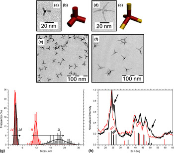
Figures 1(a) and 1(c) show bright field (BF) TEM images of CdTe tetrapod-shaped seeds with arm length of 12 ± 1 nm and width of 3.0 ± 0.7 nm. CdTe nanocrystals had a high degree of shape homogeneity and size distribution of about 10–20%. Colloidal CdTe/CdSe nanocrystal heterostructures were grown by a similar procedure as described in Refs. Reference Vasiliev, Dirin, Sokolikova, Dorofeev, Vitukhnovsky and Gaskov21 and Reference Dirin, Vasiliev, Sokolikova and Gaskov22 but at stoichiometric 1:2 [Cd]:[oleic acid] precursors molar ratio. This ratio corresponds to oleic acid consumption on cadmium oleate formation and absence of free oleic acid in the reaction mixture. It was shown by TEM [Figs. 1(d) and 1(f)] that used synthesis conditions promoted CdSe-oriented growth at the ends of CdTe arms along the [0001] crystallographic direction. This led to arm elongation by two times without substantial thickening [Fig. 1(g)]. Selective growth of CdSe tips out of the arms of CdTe tetrapod seeds was confirmed by XRD data. Figure 1(h) shows powder diffraction pattern collected on CdTe/CdSe heterostructures as well as corresponding pattern of CdTe seeds. The arrows indicate the most evident differences between two patterns. Here, an increase in the intensity at 2θ angles of 26° [(002) reflection of CdSe] and 50° [(112) reflection of CdSe] was clearly observed, indicating the formation of CdSe tips. Note that (002) reflection of CdSe and (101) reflection of CdTe are strongly overlapped but (10l) reflections of CdTe nanocrystals are dampened usually,Reference Fiore, Mastria, Lupo, Lanzani, Giannini, Carlino, Morello, De Giorgi, Li, Cingolani and Manna23 suggesting that increase in the intensity at 26° originates mainly from narrow (002) reflection of anisotropic CdSe tips. As the tip is grown, the diffraction peaks shift toward larger 2θ that indicates compression of the lattice planes in CdTe core.
Transmission electron microscopy (TEM) images show (a) CdTe tetrapod seed and (c) its ensemble as well as (d) typical CdTe/CdSe nanocrystal heterostructure and (f) its ensemble. The schematics of (b) initial CdTe and (e) final CdTe/CdSe nanocrystal heterostructure are also shown. The particles are not aggregated. (g) Size histogram of arm width (d) and length (l) for initial CdTe tetrapods (1, red) and CdTe/CdSe heterostructures (2, black). (h) Powder x-ray diffraction patterns of CdTe tetrapods (red line) and CdTe/CdSe heterostructures (black line). The arrows indicate the most evident differences.

It was shown earlierReference Vasiliev, Dirin, Sokolikova, Dorofeev, Vitukhnovsky and Gaskov21, Reference Dirin, Vasiliev, Sokolikova and Gaskov22 that the presence of free oleic acid led to concentric shell growth around tetrapod arms without significant arm elongation. We propose that free oleic acid breaks CdSe growth on CdTe arm ends. This agrees well with tetrapod crystallographic structure,Reference Manna, Scher and Alivisatos4 rigorously described growth mechanism,Reference Manna, Scher and Alivisatos4, Reference Peng and Peng24 and the previously reported n-octadecylphosphonic acid concentration influence on CdTe tetrapods growth.Reference Manna, Milliron, Meisel, Scher and Alivisatos25 In the presence of free stabilizer molecules, the Cd (0001) facet is effectively passivated and growth in this direction is strongly inhibited. In the absence of free stabilizer, this facet may have dangling bonds and higher growth rate on (0001) facet is favored relative to {hkl0} ones.
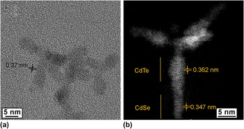
BF HRTEM image [Fig. 2(a)] of CdTe tetrapods utilized as a seed for CdSe growth demonstrates well-resolved stacking sequences of planes along the arms, with random transitions from a zinc blende type (ABCABC...) to a wurtzite type (ABAB...). Such a high density of stacking faults is quite obvious for tetrapods and rods in which the arms are made of CdTe,Reference Fiore, Mastria, Lupo, Lanzani, Giannini, Carlino, Morello, De Giorgi, Li, Cingolani and Manna23 and it has also been observed extensively in the growth of CdTe thin films.Reference Yan, Al-Jassim, Jones, Wei and Zhang26 The interplanar distance obtained from lattice images of CdTe in zone axis perpendicular to c-axis was c/2 = 0.37 ± 0.01 Å. Figure 2(b) shows an HAADF HRSTEM image of a representative CdTe/CdSe tetrapod. Minor variation (<2 monolayers) of arm width was observed along the long-axis direction. The length of thick part correlates with CdTe arm length. Arm width variation may correspond to both partial overcoating of lateral arm facets and Ostwald ripening at their end as was shown for CdTe tetrapods.Reference Manna, Milliron, Meisel, Scher and Alivisatos25 The contrast of the HAADF HRTEM image is strongly related to the average atomic number of the specimen and to its thickness. Thus, the brighter area in Fig. 2(b) corresponds to the CdTe part of the arm. Close inspection of the images demonstrated difference in the interplanar distance c/2 along the tip axis: these are 0.362 ± 0.012 nm for CdTe and 0.347 ± 0.012 nm for CdSe parts. It should also be noted that in the CdSe portion of the tips, similar stacking faults were observed. In any case, continuous stacking sequence indicates epitaxial growth of CdSe tips on the CdTe arms. Short-axis constants are also estimated: a = 4.1 ± 0.1 Å for CdSe; a = 5.1 ± 0.2 Å for CdTe. These values are close to those reported previously for bulk CdSe and CdTe wurtzite structures: c is 7.011 and 7.4512 (calculated) for CdSe and CdTe, respectively; a is 4.3 and 4.5499 (calculated) for CdSe and CdTe, respectively.Reference Wei and Zhang27 Note that for CdSe, the measured lattice constant a was less than that for bulk CdSe but the opposite relation was found for CdTe.
(a) Bright field high-resolution TEM (HRTEM) image of initial CdTe tetrapod seeds. (b) High-angle annular dark-field HRSTEM image of CdTe/CdSe heterostructure. Examination of a linear junction between CdTe (upper part of bottom arm) and CdSe (lower part of bottom arm) reveals continuous epitaxial growth. The lattice distances are indicated.

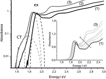
Optical absorption measurements of tetrapod seeds show a distinct CdTe excitonic absorption band near 1.93 eV with full width at half maximum (FWHM) of 96 meV. CdSe growth caused monotonous shift of CdTe excitonic absorption maximum to longer wavelengths and slight variation of its absorbance (Fig. 3). On reaching a certain length of CdSe, a low-energy feature appeared in the absorption spectrum. This feature has absorbance an order of magnitude lower than the CdTe excitonic band and may correspond to charge-transfer band of the spatially separated electron and hole because low absorbance indicates weak overlap of electron and hole wave functions.Reference Ivanov, Nanda, Piryatinski, Achermann, Balet, Bezel, Anikeeva, Tretiak and Klimov15 It should be noted that analogous absorption feature was observed in Ref. Reference Scholes, Jones and Kumar19 for CdTe/CdSe nanorod heterostructures but was not found for seeded-grown CdSe/CdTe as well ZnTe/CdTe tetrapod heterostructures, probably due to small size of heterostructure core.Reference Fiore, Mastria, Lupo, Lanzani, Giannini, Carlino, Morello, De Giorgi, Li, Cingolani and Manna23 Energy difference between CdTe excitonic and charge-transfer bands was about 80 meV for maximal CdSe length. At the same time, absorption far above the band edge (3.1 eV) increased during nanocrystal growth because of linear superposition of absorption per ion pair unit at these energies similarly to absorbance behavior of monocomponent nanocrystals reported in Ref. Reference Donega and Koole28.
The absorption spectra of a CdTe tetrapod seeds (1) and CdTe/CdSe tetrapod-shaped heterostructures with 5 nm (2) and 9 nm (3) CdSe tips. Gaussian bands corresponding to CdTe excitonic absorption band and charge-transfer band, retrieved from fitting spectra, are shown. Consecutive absorption spectra of heterostructure series during CdSe tips growth are shown in the inset.

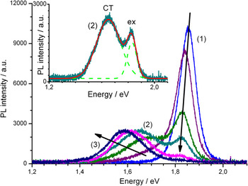
Evolution of sample luminescence during CdSe growth is represented in Fig. 4. Initial CdTe seeds demonstrated very weak luminescence (not shown) with quantum yield less than 1%. Just after growth started, a distinctive CdTe excitonic luminescence was observed and luminescence intensity increased gradually owing to passivation of surface-dangling bonds. At the same time, luminescence maximum shifted to the lower energy. As luminescence maximum reached about 1.85 eV, it splits into two subbands. The first one shows continuous evolution of initial excitonic band and maintains original width (FWHM is 77 meV) and, therefore, may be related to excitonic state in CdTe core. The new wide (FWHM is 207 meV) band appears in the lower energy side (1.67 eV) of spectrum. This band correlates with weak charge-transfer absorption and may be related to the recombination from the spatially separated electron and hole near CdTe–CdSe interface. This observation correlates with dataReference Scholes, Jones and Kumar19 for CdSe/CdTe nanorods. CdTe excitonic subband position slightly changed to 1.82 eV while charge-transfer subband shifted to lower energy down to 1.58 eV (about 0.3 eV relative to initial CdTe seeds). Splitting energy ΔE increased from 80 to 260 meV in accordance with the length of the grown CdSe. Charge-transfer luminescence involves electron state that is mostly confined in four CdSe tips, probably close to CdTe/CdSe interface. Note that in spite of long distance from tetrapod center to interface plane (∼12 nm), the formation of type II carriers’ localization regime was observed for CdTe/CdSe tetrapods, which suggests the possibility of localization of both carriers into the same arm.
Photoluminescence spectra of CdTe/CdSe tetrapod-shaped nanocrystal heterostructures with different CdSe tip length. Arrows show spectra modification during tip growth. Redistribution of dual luminescence intensity is clearly seen. Samples (1)–(3) are the same as in Fig. 3. Inset shows the photoluminescence spectrum of sample (2) fitted by two Gaussians.

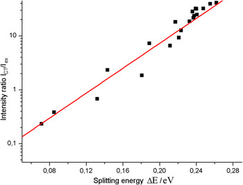
An interesting effect was observed in behavior of subbands luminescence intensity variation after splitting. We found that the ratio of luminescence intensities of subbands changed during CdSe growth. Intensity of charge-transfer band I CT increased as intensity of CdTe excitonic band I ex decreased. Such behavior indicates coupling of spatially separated CdTe excitonic and CdTe/CdSe charge-transfer states. Measured intensity ratio I CT/I ex of these subbands exponentially depends on splitting energy (Fig. 5). This effect may relate to exciton populations controlled by the energy difference between charge transfer and CdTe excitonic level positions.
Charge-transfer luminescence band intensity I CT with respect to CdTe excitonic luminescence band intensity I ex in dependence on splitting energy. Line is the fitting result according to exponential law.

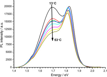
Strong redistribution of luminescence intensities was found to be sensitive to temperature-dependent band positions as well. We tested the modification of photoluminescence spectrum with temperature from 10 to 60 °C. There was considerable (up to two times) variation of charge-transfer band intensity and moderate (∼10%) variation of CdTe excitonic band intensity (Fig. 6). However, this effect cannot be attributed to temperature change solely because of noticeable shifts of both luminescence bands’ maximum position. Net value of the change of splitting energy reached 30 meV, which is comparable with splitting energy change owing to the growth of CdSe tips as plotted in Fig. 5. The fact that photoluminescence spectrum of the certain sample may be considerably modified with temperature suggests practical applications as luminescence-based temperature sensors.
Photoluminescence spectra of CdTe/CdSe tetrapod-shaped nanocrystal heterostructures collected at temperatures in the range of 13–53 °C.

IV. CONCLUSIONS
Using colloidal CdTe/CdSe tetrapod-shaped heterostructures with CdSe tips grown selectively on the end of CdTe arms, we studied the evolution of optical properties during the gradual increase in tip volume for the first time.
Selective CdSe growth at the ends of CdTe arms in [0001] crystallographic direction has been achieved at Cd:oleic acid precursors molar ratio of 1:2. Absence of free oleic acid maintains rapid growth of high-energetic (0001) facet in contrast to condition of free surfactant presence, which breaks growth in [0001] direction. HAADF HRSTEM investigation confirms the continuous stacking sequence along the CdTe/CdSe arm.
We have shown that formation of CdSe tips causes not only red-shift of excitonic band, which is typical for nanocrystal heterostructures, but also the appearance of two different bands in absorption as well as luminescence spectra. The first one is attributed to CdTe excitonic band, whereas the second one is attributed to charge-transfer band, which corresponds to spatially separated electron-hole pairs. We found that the ratio of charge transfer and CdTe excitonic luminescence intensities varies with CdSe tip length and depends on the energy difference between the respective levels. Redistribution of luminescence was found also with temperature variation.
ACKNOWLEDGMENT
This work was partially supported by the Russian Foundation for Basic Research (RFBR) Grants Nos. 07-03-00843 and 09-02-00546.