I. INTRODUCTION
Transient liquid phase (TLP) bonding is a very promising technology for chip bonding and chip stacking in a three-dimensional (3D) packaging process. Reference Munding, Hübner, Kaiser, Penka, Benkart, Kohn, Tang, Gutmann and Reif1 This bonding process, also known as solid–liquid interdiffusion (SLID) bonding, can be processed at relatively low temperatures while resulting in higher re-melting temperatures of the produced joints which fully consist of intermetallic compounds (IMCs). Reference Humpston and Jacobson2,Reference Cook and Sorensen3 On heating, the interlayer melts and solidifies as a result of interdiffusion with the substrates. It has the advantage of not requiring high pressures needed in typical solid state diffusion bonding processes. Several TLP bonding schemes have been developed to join base metals Cu, Au, Ag, Ni, Pd, Zr, and Pt using Sn or In foils of 5–100 μm in thickness as interlayers. Reference Munding, Hübner, Kaiser, Penka, Benkart, Kohn, Tang, Gutmann and Reif1–Reference Li, Agyakwa and Johnson9 Among them, Cu–Sn and Ni–Sn TLP bonding schemes have distinct advantages over the others, such as forming high re-melting temperature IMCs, cost effective, compatible with manufacturing, and commonly used elements in electronic packaging. However, an inherent drawback for the conventional TLP processes is that they all necessitate a very long bonding time for complete consumption of interlayer melts, especially for the Ni–Sn system. Moreover, the Cu–Sn system would experience the transformation process from high-temperature hexagonal η-Cu6Sn5 to low-temperature monoclinic η′-Cu6Sn5 at equilibrium temperature 186 °C and from Cu6Sn5 to Cu3Sn which brings in serious reliability concern for the formation of massive Kirkendall voids. Reference Li, Agyakwa and Johnson9–Reference Ho, Yang and Kao11
In recent years, Cu–Ni cross-interaction in solder joints has attracted a wide attention. Reference Ho, Yang and Kao11–Reference Huang, Hsiao, Chen and Tu13 Studies have indicated that the interfacial reactions in the Cu/solder/Ni sandwich structure are different from those of single Cu/solder and Ni/solder systems. Reference Ho, Yang and Kao11,Reference Wang and Liu12 For example, the Ni3Sn4 phase is the primary IMC that forms at the Ni/Sn interface, while the (Cu,Ni)6Sn5 phase becomes the primary IMC phase on the Ni side of the Cu/Sn/Ni sandwich structure. Reference Wang and Liu12 Both Cu and Ni atoms could diffuse across the entire liquid solder layer to the opposite sides of the sandwich structure in a very short time during the soldering process. The diffusion of Cu to the Ni side could form a single layer of (Cu,Ni)6Sn5 or a bilayer of (Cu,Ni)6Sn5 and (Ni,Cu)3Sn4 over the Ni substrate and the diffusion of Ni to the Cu side could form a layer of (Cu,Ni)6Sn5 over the Cu substrate. Cu–Ni cross-interaction accelerates the growth of IMCs and the consumption of substrates. Reference Ho, Yang and Kao11 With the diameter of solder bumps downsizing from current 100 to 1 μm in the future Reference Hsiao, Liu, Lin, Liu, Lu, Huang, Chen and Tu14 and the diffusion or reaction distance continually decreasing, the Cu–Ni cross-interaction becomes more significant since the driving force for the cross-interaction process is a chemical potential gradient or chemical force. Reference Huang, Hsiao, Chen and Tu13
Meanwhile, recent experimental studies by several research groups consistently showed that thermomigration (TM) occurred in solder joints when reflowing under a certain temperature gradient, resulting in a different interfacial reaction behavior between the cold and hot ends of the solder joints. Reference Chen, Hsiao, Chang, Ouyang and Tu15–Reference Zhao, Zhong, Huang, Ma and Dong20 That is, the consumption of Cu or Ni substrates at the hot end was significantly accelerated, whereas that at the cold end was inhibited. At the same time, the growth of the IMCs at the cold end was abnormally fast while that at the hot end was strongly restrained.
Since both TM and Cu–Ni cross-interaction can accelerate the IMC growth, how the coupling effect of TM and Cu–Ni cross-interaction affects the interfacial microstructure of microinterconnect deserves detailed studies. However, few data are available and thus an in-depth study needs to be carried out. In the present work, the evolution of IMCs in Cu/Sn/Ni ultrafine interconnects during soldering under a temperature gradient was investigated. The coupling effect of TM and cross-interaction on the IMC growth at both cold and hot ends was discussed. A new TLP bonding process with high bonding speed and stable IMCs was proposed based on the developed method.
II. EXPERIMENTAL
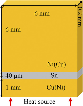
Cu/Sn/Ni sandwich structure specimens were prepared by immersion soldering at 250 °C for 20 s. Cu (99.95%) and Ni (99.99%) plates were prepared with one surface being carefully grounded, polished, and cleaned in ethanol. After the polished faces were aligned and fixed, the whole configuration was immersed into a pure Sn (99.99%) bath. The gap between the Cu and Ni plates was controlled by two spacers. After immersion soldering, the specimen was cooled immediately in water to room temperature and cut into individual Cu/Sn/Ni microjoints following by grinding and polishing. The Sn solder layer between the Cu and Ni substrates was about 40 μm in thickness. TLP bonding experiments under the temperature gradient were carried out by reflowing the interconnects on a hot plate exposed to air at 250 °C for different durations. Figure 1 shows the schematic of the TLP bonding experiments under the temperature gradient. Silicone grease with a high thermal conductivity was used to fix the interconnects onto the hot plate. For comparison, isothermal TLP bonding experiments were conducted in an Espec STH-120 high-temperature chamber at 250 °C for same reaction durations.
Schematic of the TLP bonding experiments under temperature gradient.

The microstructure of the Cu/Sn/Ni ultrafine interconnects after TM and isothermal TLP bonding was analyzed using a scanning electron microscope (SEM) equipped with an energy dispersive X-ray (EDX) spectrometer. Electron probe microanalysis (EPMA) was used to identify the compositions of the phases. The temperature distribution in the liquid solder layer was simulated by computational fluid dynamics (CFD).
III. RESULTS AND DISCUSSION
A. Simulation of temperature distribution in the liquid solder layer
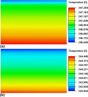
As the Cu/Sn/Ni interconnects were too small to directly measure the temperature difference between the two interfaces, CFD was utilized to simulate the temperature distribution in the liquid solder layer. The thermal conductivities of Cu, Ni, molten Sn, and silicone grease used for the simulation were 401.0, Reference Incropera and DeWitt21 90.7, Reference Incropera and DeWitt21 30.7, Reference Peralta-Martinez and Wakeham22 and 4.5 W/m·K, respectively. The effective thickness of the silicone grease layer was set to be 100 μm. The ambient temperature and gravity vector were set to be 20 °C and −9.81 m/s2, respectively. The cabinet for calculation was 400 × 400 × 400 mm in dimension. The Boussinesq approximation and zero equation of turbulence were used to model the natural convection. The bottom interface close to the hot plate was defined as the hot end and the top interface was defined as the cold end.
Figure 2 shows the simulated temperature distribution in the liquid solder layers during reflow on the hot plate. Though Cu has a much higher thermal conductivity than Ni, the simulated results show a small difference in temperature distribution when Cu and Ni substrates are the hot end, respectively. The temperature difference across the liquid solder layers was about 0.6 °C for both conditions. Accordingly, a temperature gradient of 150 °C/cm was established in the ultrafine interconnects.
Simulated temperature distribution in the liquid solder layers during reflow on the hot plate with (a) Cu and (b) Ni as the hot end, respectively.

B. Microstructure of as-soldered interconnect
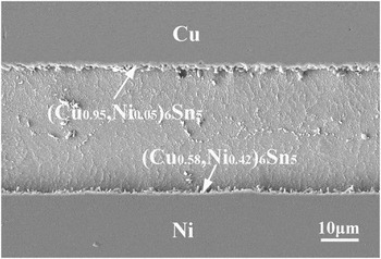
Figure 3 shows the cross-sectional microstructure of an as-soldered Cu/Sn/Ni ultrafine interconnect. The presence of the Cu signals on the Ni side and the Ni signals on the Cu side was identified by EPMA. A cross-interaction between Cu and Ni readily occurred within 20 s with a 40-μm-thick Sn separation layer when the interconnect was fabricated at 250 °C. The diffusion of Cu to the Ni side resulted in the formation of facet-like (Cu0.58Ni0.42)6Sn5 IMCs over the Ni substrate, and the presence of Ni on the Cu side produced a continuous thin (Cu0.95,Ni0.05)6Sn5 layer over the Cu substrate, instead of the typical scallop-like Cu6Sn5. Additionally, many particles with size ranging from submicron scale to several microns scattered in the Sn solder matrix. These particles were identified to be Cu6Sn5 with a small amount of Ni and were believed to be the precipitates formed during solidification, due to the limited solubilities of Cu and Ni in solid Sn.
Cross-sectional microstructure of an as-soldered Cu/Sn/Ni ultrafine interconnect.

C. Evolution of interfacial IMCs during isothermal TLP bonding
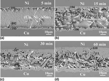
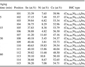
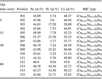
Figure 4 shows the cross-sectional microstructure of the Cu/Sn/Ni ultrafine interconnects after isothermal TLP bonding at 250 °C for different durations. The compositions of the IMCs at different positions as marked in Fig. 4 are listed in Table I. The interfacial IMCs gradually grew thicker with increasing reaction duration, whereas the asymmetrical growth of the interfacial IMCs between the Cu and Ni sides was observed, i.e., the IMC growth at the Cu side was obviously slower than that at the Ni side. Meanwhile, the IMC morphology and composition between the Cu and Ni sides were both in significant difference. After bonding for 5 min, Cu atoms dissolved into the solder and diffused to the opposite Ni side, resulting in the interfacial IMCs transforming from the initial facet-like (Cu0.58,Ni0.42)6Sn5 into rod-like (Cu0.88,Ni0.12)6Sn5. Similarly, the dissolution and diffusion of Ni atoms resulted in the formation of a continuous (Cu0.89,Ni0.11)6Sn5 layer instead of (Cu0.95,Ni0.05)6Sn5 at the Cu side. Additionally, some (Cu0.88,Ni0.12)6Sn5 IMC particles were detected in the solder matrix. After bonding for 15 min, bulky rod-like (Cu0.86,Ni0.14)6Sn5 IMCs formed at the Ni side and scallop-like (Cu0.92,Ni0.08)6Sn5 IMCs formed at the Cu side. Plenty of hollow rod-like (Cu0.87,Ni0.13)6Sn5 IMCs were observed in the solder matrix. After bonding for 30 min, the IMCs formed at the Ni and Cu sides were (Cu0.80,Ni0.20)6Sn5 and (Cu0.94,Ni0.06)6Sn5, respectively. With increasing bonding time to 60 min, the interfacial IMCs from the two interfaces along with the IMCs in the solder matrix even had merged together at some regions. With the EPMA points stepping from the Cu side to the Ni side, the Ni concentration increased while the Cu concentration decreased in the IMCs. A strong Cu–Ni cross-interaction occurred in the ultrafine interconnects, especially at the Ni side. Moreover, the rough Cu/IMC interface indicated a serious dissolution of the Cu substrate.
Cross-sectional microstructure of the Cu/Sn/Ni ultrafine interconnects after isothermal TLP bonding at 250 °C for (a) 5 min, (b) 15 min, (c) 30 min, and (d) 60 min.

Compositions of the IMCs at different positions as marked in Fig. 4.

It is noted that there was no obvious formation of Cu3Sn at the Cu side during the reaction. It has been reported that only a small amount of Ni (0.1 wt%) participating in soldering reaction with Cu would significantly accelerate the growth of Cu6Sn5 [or (Cu,Ni)6Sn5] but decelerate that of Cu3Sn. Reference Ho, Yang and Kao11,Reference Tsai, Hu, Tsai and Kao23 The decrease in Cu3Sn would substantially improve the drop reliability due to the reduction in the growth of Kirkendall voids as a function of Cu3Sn thickness. Reference Huang, Wu, Lai and Chan10,Reference Ho, Yang and Kao11 In addition, the growth rate of the (Cu,Ni)6Sn5 IMCs at the Ni side was much higher than that at the Cu side, which was attributed to the large amount of Cu atoms continually diffusing from the Cu side to the opposite Ni side. Cu–Ni cross-interaction plays a significant effect on the IMC growth in the Cu/Sn/Ni ultrafine interconnects during isothermal bonding.
D. Evolution of interfacial IMCs during TLP bonding under temperature gradient
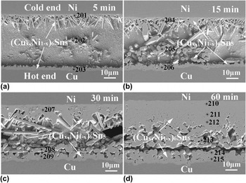
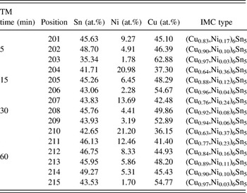
Figure 5 shows the cross-sectional microstructure of the Cu/Sn/Ni ultrafine interconnects after TLP bonding under the temperature gradient for different durations with the Cu substrate as the hot end. The compositions of the IMCs at different positions as marked in Fig. 5 are listed in Table II. Compared with the isothermal aging cases, the asymmetrical growth of the IMCs at the two interfaces became more obvious. After bonding for 5 min, ragged needle-like (Cu0.83,Ni0.17)6Sn5 IMCs precipitated at the Ni cold end and a laminar scallop-like (Cu0.97,Ni0.03)6Sn5 IMCs precipitated at the Cu hot end. Additionally, plenty of rod-like (Cu0.90,Ni0.10)6Sn5 IMCs were observed in the solder matrix. After bonding for 15 and 30 min, the IMCs at the Ni cold end grew fast toward the Cu hot end, while those at the Cu hot end grew relatively slowly. Masses of (Cu,Ni)6Sn5 IMCs precipitated in the solder matrix, indicating a very strong Cu–Ni cross-interaction. After bonding for 60 min, the IMCs from the Ni cold end had merged with those in the matrix and almost met the opposite IMCs with a narrow gap in between. The temperature gradient enhanced the Cu–Ni cross-interaction and thus the IMC growth at the Ni cold end. Moreover, no obvious Cu3Sn formation was detected at the Cu hot end.
Cross-sectional microstructure of the Cu/Sn/Ni ultrafine interconnects after TLP bonding under temperature gradient at 250 °C for (a) 5 min, (b) 15 min, (c) 30 min, and (d) 60 min. The Cu substrates were the hot end.

Compositions of the IMCs at different positions as marked in Fig. 5.

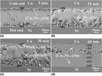
Figure 6 shows the cross-sectional microstructure of the Cu/Sn/Ni ultrafine interconnects after TLP bonding under the temperature gradient at 250 °C for different durations with the Ni substrate as the hot end. The compositions of the IMCs at different positions as marked in Fig. 6 are listed in Table III. After bonding for 5 min, the IMC morphology was similar with the isothermal aging case, i.e., rod-like (Cu0.83,Ni0.31)6Sn5 IMCs precipitated at the Ni/Sn interface (hot end) and a continuous (Cu0.97,Ni0.10)6Sn5 IMC layer formed at the Cu/Sn interface (cold end). Some (Cu0.87,Ni0.13)6Sn5 IMC particles were also observed in the solder matrix. However, after bonding for 15 and 30 min, plenty of promiscuous needle-like (Cu,Ni)6Sn5 IMCs formed at the Ni hot end and rod-like (Cu,Ni)6Sn5 IMCs, instead of the scallops in the cases of isothermal aging, abnormally precipitated at the Cu cold end. With increasing bonding time to 60 min, the IMCs from the two interfaces had merged together. However, the IMCs at the Ni hot end were much denser and thicker than those at the Cu cold end. The temperature gradient enhanced the Cu–Ni interaction and thus the IMC growth at the Ni hot end. Moreover, no obvious Cu3Sn formation was detected at the Cu cold end.
Cross-sectional microstructure of the Cu/Sn/Ni ultrafine interconnects after TLP bonding under temperature gradient at 250 °C for (a) 5 min, (b) 15 min, (c) 30 min, and (d) 60 min. The Ni substrates were the hot end.

Compositions of the IMCs at different positions as marked in Fig. 6.

It should be noted that in spite of Cu or Ni as the hot end, the Cu substrates were consumed more seriously than the Ni substrates, evidenced by the rougher Cu/IMC interface and the higher Cu concentration in the IMCs; however, the growth of the (Cu,Ni)6Sn5 IMCs at the Sn/Ni interfaces was always much faster. Moreover, the Ni concentration increased while the Cu concentration decreased in the IMCs with the EPMA points stepping from the Cu substrate to the Ni substrate. Apparently, the additional temperature gradient had a significant influence on the Cu–Ni cross-interaction and their coupling effect remarkably affected the interfacial reactions in the Cu/Sn/Ni ultrafine interconnects during the reflow process.
E. Coupling effect of TM and cross-interaction on IMC evolution
The composition, morphology, and thickness of the (Cu,Ni)6Sn5 IMC in the Cu/Sn/Ni ultrafine interconnects depend strongly on the temperature gradient (Figs. 4–6 and Tables I–III). The essential cause of such dependence could be attributed to the different amounts of Cu and Ni atomic fluxes being introduced into the solder. The driving force of TM F is given as Reference Chen, Hsiao, Chang, Ouyang and Tu15
 $$F = - {{Q*} \over T}\left( {{{\partial T} \over {\partial x}}} \right)\quad ,$$
where Q* is the heat of transport, T is temperature, and ∂T/∂x is the temperature gradient. Taking the temperature gradient (150 °C/cm) and heat of transport (11.12 kJ/mol Reference Zhao, Zhong, Huang, Ma and Dong18 for Cu and 0.76 kJ/mol Reference Yang, Yang and Ouyang16 for Ni) into Eq. (1), the driving forces of TM in liquid Sn at 250 °C F Cu and F Ni equal to 5.30 × 10⁻¹⁹ N and 3.62 × 10⁻²⁰ N, respectively. Since F Cu is more than an order of magnitude larger than F Ni, Cu is more sensitive to the temperature gradient than Ni.
The results in this study are very different from those in our previous study where the Cu/Sn(90 μm)/Ni interconnects had a greater reaction distance and a much higher temperature gradient of 1500 °C/cm. Reference Zhong, Huang, Ma, Dong, Wang and Zhao19 In our previous study, when Ni was the hot end, both Cu and Ni atoms could diffuse to the opposite interfaces, resulting in the occurrence of Cu–Ni cross-interaction and the formation of (Cu,Ni)6Sn5 at both interfaces. However, when Cu was the hot end, only Cu atoms could diffuse to the opposite interface, resulting in the occurrence of the Cu–Ni cross-interaction only at the cold end and the formation of Cu6Sn5 the at the hot end. This is due to the fact that the driving force of the chemical potential gradient in the ultrafine interconnects is larger and that of TM is much smaller in the current study.
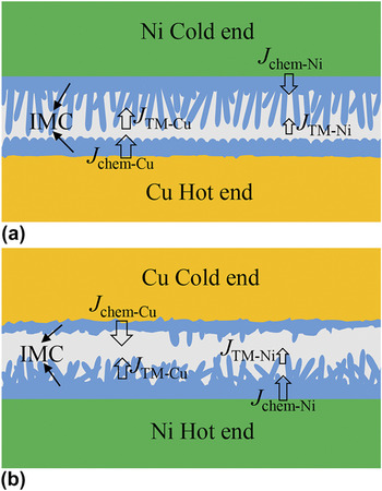
Figure 7 shows the schematics of the atomic fluxes in the Cu/Sn/Ni interconnects undergoing TLP bonding under the temperature gradient. With the Cu substrate as the hot end, as shown in Fig. 7(a), the Cu and Ni atomic fluxes, J Cu and J Ni, in the liquid Sn can be written as follows:
 $${J_{{\rm{Cu}}}} = {\rm{\ }}{J_{{\rm{chem}} ‐ {\rm{Cu}}}} + {J_{{\rm{TM}} ‐ {\rm{Cu}}}}\quad ,$$
 $${J_{{\rm{Ni}}}} = {\rm{\ }}{J_{{\rm{chem}} ‐ {\rm{Ni}}}} - {J_{{\rm{TM}} ‐ {\rm{Ni}}}}\quad ,$$
where J chem-Cu and J TM-Cu are the Cu atomic flux and J chem-Ni and J TM-Ni are the Ni atomic flux induced by the chemical potential gradient and temperature gradient, respectively.
Schematics of atomic fluxes in the Cu/Sn/Ni ultrafine interconnects undergoing TLP bonding under temperature gradient with (a) Cu and (b) Ni substrates as the hot end, respectively.

Since J chem-Cu and J TM-Cu are in the same direction, the consumption of the Cu substrate is accelerated and the diffusion of Cu atoms across the liquid Sn is significantly enhanced. However, J chem-Ni and J TM-Ni are in the opposite directions, resulting in limited consumption of the Ni substrate and a small amount of Ni atomic flux. At the Cu hot end, as Ni atoms are difficult to diffuse across the liquid Sn against the temperature gradient, the Ni concentration in the IMCs at the Cu/Sn interface is obviously lower comparing with the isothermal bonding case, as shown in Tables I and II. At the Ni cold end, massive Cu atoms migrate from the opposite side, resulting in an enhanced Cu–Ni cross-interaction and thus an abnormally fast IMC growth at the Ni/Sn interface.
In the case of the Ni substrate as the hot end, as shown in Fig. 7(b), the Ni and Cu atomic fluxes, J Cu and J Ni, in the liquid Sn can be written as follows:
 $${J_{{\rm{Cu}}}} = {J_{{\rm{chem}} ‐ {\rm{Cu}}}} - {J_{{\rm{TM}} ‐ {\rm{Cu}}}}\quad ,$$
 $${J_{{\rm{Ni}}}} = {J_{{\rm{chem}} ‐ {\rm{Ni}}}} + {J_{{\rm{TM}} ‐ {\rm{Ni}}}}\quad .$$
Since J chem-Cu and J TM-Cu are in the opposite directions, the diffusion of Cu atoms across the liquid Sn to the Ni hot end should be significantly retarded. However, J chem-Ni and J TM-Ni are in the same direction, resulting in an enhanced diffusion of Ni atoms from the Ni hot end toward the Cu cold end. With a profused Ni concentration, the Cu solubility in the molten Sn can be dramatically reduced, Reference Ho, Yang and Kao11 which enlarges the J chem-Cu item much over the J TM-Cu item and thus causes a large total Cu atomic diffusion flux J Cu. As a result, the consumption of the Cu cold end becomes comparable with the Cu hot end case. At the Cu hot end, the high Ni concentration (Table III) leads to the transformation of IMC morphology from scallop-like to rod-like. At the Ni hot end, a mass of the dissolved Cu atoms can diffuse countering a temperature gradient to the Ni/Sn interface under an enlarged J chem-Cu, which maintains the interfacial IMCs still as (Cu,Ni)6Sn5. Under this circumstance, the interfacial IMCs at the hot end grow even abnormally faster than those at the cold end.
In practice, the processes of IMC formation and dissolution can occur simultaneously. According to Dybkov’s model, Reference Dybkov24 the dissolution rate of IMC into liquid solder during reflow can be expressed as
 $${{{\rm{d}}C} \over {{\rm{d}}t}} = {K_{\rm{d}}}{S \over V}\left( {{C_{\rm{s}}} - C} \right)\quad ,$$
where C s represent the saturated concentrations (or solubility) of the solute (i.e., Cu or Ni) in the solder, K d is the dissolution rate constant, S is the area of solid in contact with liquid solder, and V is the solder volume.
According to Eq. (6), the dissolution rate of interfacial IMC into liquid solder is proportional to C s − C. Therefore, the higher the C s − C is, the faster the interfacial IMC dissolves. The IMC formation occurs when the local concentration at the interface region exceeds C s. At the same time, the solute (e.g., Cu or Ni) near the interface region continues to diffuse outward because of the concentration gradient or temperature gradient, and the local concentration at the interface region drops below C s as a result. This causes the dissolution of the newly formed IMCs to maintain equilibrium with the molten solder. The dissolution slows down while the growth of the IMC continues when C becomes approximately equal to C s. At this stage, the IMC growth becomes the dominant contributor to substrate consumption.
The reaction products at Sn/Ni interface are particularly sensitive to the Cu concentration in Sn-based solders and the growth of (Cu,Ni)6Sn5 becomes dominant when the Cu concentration increases to or exceeds 0.6 wt%. Reference Ho, Yang and Kao11,Reference Wang and Liu12 In this work, the presence of the abnormally thick and dense (Cu,Ni)6Sn5 layer at the Sn/Ni interfaces suggests that the Cu concentration reaches a relatively high level. Moreover, the large (Cu,Ni)6Sn5 precipitations in the solder matrix and the formation of (Cu,Ni)6Sn5 IMCs at the Cu hot end indicate that the Ni concentration in the solder also reaches a high level. The temperature gradient causes mass TM of Cu and Ni atoms and further enhances the Cu–Ni cross-interaction in Cu/Sn/Ni the ultrafine interconnects. Under the coupling effect of TM and Cu–Ni cross-interaction, the dissolution of the Cu substrates is more serious while the growth of the (Cu,Ni)6Sn5 IMCs at the Sn/Ni interface is abnormally fast.
Ouyang et al. reported that Ni3Sn4 IMC with a total thickness of 6.54 μm formed in Ni/SnAg(50 μm)/Ni interconnects after soldered under a temperature gradient of 160 °C/cm at 260 °C for 60 min. Reference Yang, Yang and Ouyang16 Our previous study found that Cu6Sn5 IMC with a total thickness of 29.95 μm formed in Cu/Sn(200 μm)/Cu interconnects after soldered under a temperature gradient of 135 °C/cm at 250 °C for 60 min. Reference Zhao, Zhong, Huang, Ma and Dong18 While in the present study, under the coupling effect of TM and cross-interaction, the Cu/Sn(40 μm)/Ni interconnects almost fully consist of (Cu,Ni)6Sn5 IMC after soldered under a temperature gradient of 150 °C/cm at 250 °C for 60 min regardless of the direction of the temperature gradient. The growth of the dense (Cu,Ni)6Sn5 IMC is significantly accelerated while the formation of Cu3Sn is eliminated. Both are benefit to the TLP bonding process.
In addition, it has been reported that when Ni is present at 4.6–17.2 at.%, the high-temperature hexagonal η-Cu6Sn5 does not transform to the low-temperature monoclinic η′-Cu6Sn5 at the equilibrium temperature of 186 °C and the hexagonal phase remains stable from room temperature to 250 °C. Reference Nogita, Mu, McDonald, Read and Wu25 The allotropic transformation from η to η′ during solid cooling is expected to introduce internal stresses due to the volume change of transformation. Also, the presence of Ni can decrease the magnitude of thermal expansion of IMCs and prevents the discontinuity in expansion that occurs with the polymorphic transformation. Reference Mu, Read, Yang and Nogita26 Therefore, the reliability of the Cu/(Cu,Ni)6Sn5/Ni TLP interconnects would benefit from the stabilization of hexagonal (Cu,Ni)6Sn5 IMC.
IV. CONCLUSION
(Cu,Ni)6Sn5 IMCs were the predominant reaction product in the Cu/Sn/Ni ultrafine interconnects regardless of the direction of the temperature gradient. However, the composition, morphology, and thickness of the (Cu,Ni)6Sn5 IMCs depended strongly on the TM and Cu–Ni cross-interaction. The essential cause of such dependence was attributed to the different amounts of Cu and Ni atomic fluxes being introduced into the solder. When Cu was the hot end, mass Cu was found to be driven to the Ni cold end due to the combination of chemical-potential-induced Cu flux and TM-induced Cu flux, resulting in an enhanced Cu–Ni cross-interaction and thus a fast IMC growth. When Ni was the hot end, under the coupling effect of TM and Cu–Ni cross-interaction, the dissolution of the cold Cu end was more serious and the (Cu,Ni)6Sn5 IMCs at the Ni hot end grew abnormally fast. The consumption of the Ni substrate was limited while that of Cu substrates was serious even at the cold end, since Cu was found to be more sensitive to the temperature gradient. By reflowing Cu/Sn/Ni ultrafine interconnects under the temperature gradient which applies to both situations with Ni or Cu at the hot end, a new TLP bonding process was developed, with the advantages of high bonding speed, elimination of Cu3Sn and stable (Cu,Ni)6Sn5 IMC.
ACKNOWLEDGMENTS
This work was supported by the National Natural Science Foundation of China (Grant Nos. 51675080 and 51571049), the Key Laboratory of Advanced Display and System Applications (Shanghai University) (Grant No. P201601), and the Ministry of Education and the China Scholarship Council (Grant No. 201606065047).