Introduction
Organic electronics are advancing to devices beyond flexible electronics. This trend opens the pathway to stretchable electronics, where the electronic devices are integrated on/in stretchable substrates. Reference Sekitani, Noguchi, Hata, Fukushima, Aida and Someya1 Since the initial implementation of this technology, much attention has been given to the development of stretchable conductors, Reference Sekitani, Noguchi, Hata, Fukushima, Aida and Someya1–Reference Oh, Kim, Baik and Jeong3 e-skin sensors, Reference Lipomi, Vosgueritchian, Tee, Hellstrom, Lee, Fox and Bao4–Reference You, Kim, Park, Koh, Shin, Jung and Jeong6 light-emitting diodes, Reference Sekitani, Nakajima, Maeda, Fukushima, Aida, Hata and Someya7 energy-storage devices, Reference Gaikwad, Zamarayeva, Rousseau, Chu, Derin and Steingart8 and solar cells. Reference Lipomi, Tee, Vosgueritchian and Bao9 Although stretchable field-effect transistors are the fundamental building blocks of most stretchable devices, Reference Sekitani, Noguchi, Hata, Fukushima, Aida and Someya1,Reference Chortos, Lim, To, Vosgueritchian, Dusseault, Kim, Hwang and Bao10,Reference Shin, Song, Lim, Lim, Park and Jeong11 they have been less studied due to a lack of stretchable semiconductors. Further exploration of organic stretchable semiconductors is necessary to bring stretchable transistors into practical use.
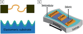
Possible methodological approaches to fabricate stretchable semiconductors are summarized in Figure 1 . The concept of imparting stretchability to organic semiconductors through geometrical engineering is shown in Figure 1a. A semiconductor in the form of a curved-line bridging two electrodes and mounted on an elastomer substrate can be stretched without mechanical failure, Reference Sekitani, Nakajima, Maeda, Fukushima, Aida, Hata and Someya7 or a semiconductor film on a prestrained rubber substrate causes the structure to buckle upon releasing the stress. Reference Wu, Kustra, Gates and Bettinger12 This is straightforward and reviewed in publications that address the fabrication of Si-based stretchable devices. Reference Rogers, Someya and Huang13,Reference Kim, Ahn, Choi, Kim, Kim, Song, Huang, Liu, Lu and Rogers14 This structural approach makes it difficult to generate uniform patterning and buckling over the entire device with miniaturization, which is the major drawback of this approach. Film-type semiconductors are more desirable than the structural design for robust applications. Such stretchable film-type semiconductors are named “intrinsically stretchable” in this article. The intrinsically stretchable semiconductors allow the fabrication of stretchable devices in which all the device components are stretchable (Figure 1b), and the patterning can be achieved by printing or lithography. In addition, such intrinsically stretchable devices ensure high stretchability without any noticeable structural change. The development of stretchable semiconductor film is a key step toward deformable devices, but it is still in the conceptual stage.
Schematic representation of the different approaches used to make stretchable semiconductors. (a) An in-plane wavy pattern (upper image) or an out-of-plane buckled structure (lower image) of the nonstretchable semiconductor becomes stretchable. (b) The flat semiconductor layer is intrinsically stretchable without any noticeable structural change. Such a semiconductor is applicable to the fabrication of all-stretchable transistors.

Here, we discuss technological approaches for intrinsically stretchable polymer semiconductor films. Although low-molecular-weight organic semiconductors have the advantage of long-range order and better transport properties, Reference Pope15 their structures and properties are relatively sensitive to mechanical deformation. Polymer semiconductors are composed of a sequence of semiflexible chains that provide greater possibility of intrinsic stretchability. Reference Pope15,Reference Wu, Benight, Chortos, Lee, Mei, To, Lu, He, Tok, Chen and Bao16 Therefore, this review focuses on polymer semiconductors.
Approaches to stretchable semiconductor layers
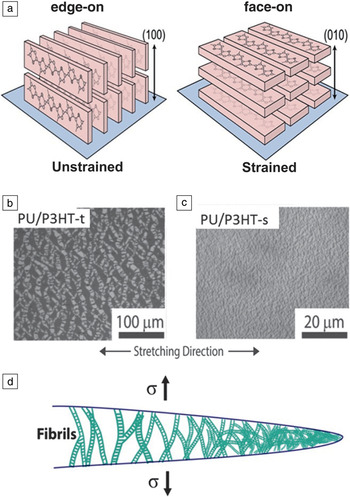
Polythiophenes are the most studied polymer semiconductors for flexible and stretchable devices. O’Connor et al. demonstrated strain-aligned anisotropic charge transport in poly(3-hexylthiophene) (P3HT) by the lamination method. Reference O’Connor, Kline, Conrad, Richter, Gundlach, Toney and DeLongchamp17 A spin-coated film of P3HT was transferred to a poly(dimethylsiloxane) (PDMS) substrate, and then strained to various extents. Upon being stretched, the crystalline P3HT polymer was aligned in the applied strain direction, along with the polymer backbone. This strain-induced alignment changes the predominant edge-on oriented (100) polymer crystallites to face-on orientation (010) ( Figure 2a). The charge mobility increased in the applied strain direction, but decreased in the perpendicular direction, causing a large anisotropy of charge mobility. On the other hand, films strained biaxially by 100% showed increased face-on alignment, but insignificant charge mobility anisotropy. Reference Gargi, Kline, DeLongchamp, Fischer, Toney and O’Connor18 Although crystallites with face-on alignment are not desired for high mobility values, starting with a film containing more face-on crystallites may enhance stretchability.
(a) Schematic illustration of the orientation of polymer crystallites with and without strain. The polymer crystallites reorient to align in the direction of applied strain, transforming the edge-on crystallites into face-on crystallites. Adapted with permission from Reference Reference Gargi, Kline, DeLongchamp, Fischer, Toney and O’Connor18. © 2013 American Chemical Society. (b–c) Effect of strain on microcrack formation in poly(3-hexylthiophene) (P3HT) films prepared by transfer from a Si wafer onto a polyurethane (PU) substrate (b) and by spin-coating on a PU substrate (c). Adapted with permission from Reference Reference Chortos, Lim, To, Vosgueritchian, Dusseault, Kim, Hwang and Bao10. © 2014 Wiley. (d) Schematic illustration of the phenomenon of crazing in ductile polymers under a stretching force σ. Upon being stretched, the polymer filaments bridge the gaps generated by the localized stress and limits them from widening.

Generally, cracks are considered as defects to be avoided, because they deteriorate the mechanical and electrical properties of a semiconductor film. However, when cracks are stable or their growth rate is slow, they are limited to micrometer-length scales. Repeated loading and unloading cycles generate new microcracks, and eventually lead to the formation of a network of ligaments that improve toughness of the material. Reference Vashishth, Tanner and Bonfield19 Bao and co-workers compared the formation of microcracks and their propagation in two P3HT thin films, one was transferred onto a polyurethane (PU) substrate and the other was directly spin-coated on the PU substrate. Reference Chortos, Lim, To, Vosgueritchian, Dusseault, Kim, Hwang and Bao10 The transferred film had 10-μm-wide microcracks under 15% tensile strain, and the microcracks propagated further at higher strains (Figure 2b). The microcracks in the spin-coated film were stable at 50% strain, and the crack width was limited at the micrometer scale, even at 200% strain (Figure 2c). When the spin-coated P3HT layer was sandwiched between two PU layers, using the top PU layer as a dielectric, the device could be operated at 265% strain, although the device charge mobility decreased in both the perpendicular and parallel directions. Reference Chortos, Lim, To, Vosgueritchian, Dusseault, Kim, Hwang and Bao10
Attaching a ductile component to a semiconducting polymer backbone can enhance the intrinsic stretchability of the material, primarily by allowing the formation of polymer filaments when the film is under large stress (Figure 2d). This phenomenon is called crazing, and is routinely observed in ductile crystalline polymers where the polymer chains have enough flexibility to align along the shear direction. The molecular filaments bridge the gaps generated by stress localization and hinder widening of the gap. Since the growth of the craze occurs prior to cracking, the craze absorbs fracture energy and effectively increases the fracture toughness of the polymer film. Lipomi and co-workers took advantage of this enhanced mechanical stability of ductile polymer semiconductors. Reference Savagatrup, Printz, Wu, Rajan, Sawyer, Zaretski, Bettinger and Lipomi20 They showed that moduli of more ductile, long-alkyl chain polythiophenes are smaller by one order of magnitude than P3HT, so the mechanical flexibility and stretchability are considerably enhanced.
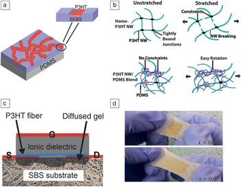
Embedding a bundle of polymer nanofibrils on an elastomer substrate increases the stretchability, because the curved contour of the bundle reduces the stress accumulation. In addition, the stress propagation is delayed in the perpendicular direction of the nanofibril bundle. Reference Prins, Grozema, Schins, Patil, Scherf and Siebbeles21 Jeong and co-workers imparted stretchability to P3HT nanofibrils by embedding them in a polystyrene-block-poly(ethylene-ran-butylene)-block-polystyrene (SEBS) elastomer matrix ( Figure 3a). Reference Shin, Oh, Byun, Lee, Kim, Baik, Park and Jeong22 When spin-coating a blend solution of P3HT and SEBS on a PDMS substrate, a thin film of the P3HT nanofibril bundles was generated on the top surface of the SEBS matrix. The in situ formation of the nanofibril bundle film was caused by the one-dimensional crystal growth of P3HT and the phase separation of P3HT to the air surface, due to the lower surface energy. Reference Shin, Oh, Byun, Lee, Kim, Baik, Park and Jeong22
(a) Schematic description of poly(3-hexylthiophene) (P3HT) nanofibrils phase-separating to the air surface from a polystyrene-block-poly(ethylene-ran-butylene)-block-polystyrene (SEBS) matrix when the mixture solution is spin-coated on a Si substrate. Adapted with permission from Reference Reference Shin, Oh, Byun, Lee, Kim, Baik, Park and Jeong22. © 2015 Wiley. (b) Schematic diagram showing the fracture mechanism in pure P3HT nanowires (NWs) (upper) and in a P3HT NW/poly(dimethylsiloxane) (PDMS) blend (bottom) under a large strain. (c–d) Schematic illustration of a nanofibril-based transistor on a polystyrene-b-polybutadiene-b-polystyrene (SBS) nanofiber mat substrate (c). All of the components in the transistor are stretchable. Digital image exhibiting the dimensional change of the device array observed by stretching at strain ε = 0.7 (d). Adapted with permission from Reference Reference Shin, Song, Lim, Lim, Park and Jeong11. © 2014 Wiley.

Cho and co-workers recently used a similar approach to prepare an intrinsically stretchable and transparent active layer by blending P3HT nanowires (NWs) and PDMS. Reference Song, Kang, Choi, Sin, Lee, Lee and Cho23 The stretchabilities of pure P3HT NWs and a blend of P3HT/PDMS (10 wt% P3HT) were compared. The blend active layer surpassed the pure P3HT NWs layer both in mobility and cyclic stability at 100% strain. This superior stretching behavior of the blended film is considered to originate from the reduced number of tight junctions formed between the P3HT NWs, and easy rotation of the P3HT NWs in the PDMS matrix (Figure 3b). Reference Song, Kang, Choi, Sin, Lee, Lee and Cho23
In a similar strategy, a network of semiconductor nanofibers can also be stretchable. Jeong and co-workers demonstrated that P3HT nanofibers electrospun on a rubbery polystyrene-b-polybutadiene-b-polystyrene nanofiber mat possess high stretchability (Figure 3c). They used Au nanosheets as a stretchable electrode and an ion gel as a gate dielectric for fabricating an all-stretchable transistor. More than 100 devices were fabricated in a single process (Figure 3d). The intrinsically stretchable transistors showed stable operation over 1500 cycles of stretching at 70%. This high stretchability and stability are attributed to the interpenetrated nanofiber networks and the diffusion of the ion gel in the porous substrate. Reference Shin, Song, Lim, Lim, Park and Jeong11
Charge transport in polymer semiconductors largely depends on the degree of structural ordering and the π-π stacking. Formation of a long-range delocalized π-molecular orbit is critical for fast charge transport. Reference Prins, Grozema, Schins, Patil, Scherf and Siebbeles21,Reference Hoofman, de Haas, Siebbeles and Warman24 In highly crystalline semiconductors, charge transport through the amorphous region between the well-ordered crystal domains requires a large activation energy. A highly crystalline polymer semiconductor is inadequate for use as a stretchable semiconductor, because stretching generates a large number of defects that act as transport barriers ( Figure 4a). Reference Yao, Dong and Hu25 Park and co-workers recently developed mechanically stable polythiophenes that also show efficient charge-carrier transport. They synthesized a low-crystalline P3HT via random copolymerization of thiophene units in the hexylthiophene backbone. The thiophene units generated localized aggregates between the well-ordered crystal domains (Figure 4b). Reference Son, Kim, Lee, Lee, Park, Noh, Park and Park26 The small aggregates in the amorphous region decreased the activation energy for charge transport through the amorphous regions and the mobility of the semiconductor polymer film can be maintained upon large stretching.
(a) Schematic representation of charge transport in a polymer semiconductor film with high crystallinity (poly(3-hexylthiophene)). (b) Charge transport in a polymer semiconductor film with a low crystallinity (a random copolymer of hexylthiophene and thiophene). Yellow arrows represent the charge-carrier pathways and the orange arrow indicates charge hopping. The insets at the bottom show the charge-carrier transport in each microstructure and corresponding polymer structures. Localized aggregates of thiophene monomers in the amorphous regions of the random copolymer lower the activation energy (E A), such that charge transport becomes insensitive to external strain. Adapted with permission from Reference Reference Son, Kim, Lee, Lee, Park, Noh, Park and Park26. © 2016 American Chemical Society. (c) Schematic of a stretchable and healable semiconducting polymer upon stretching and releasing. The small crystallites and amorphous matrix are bound with hydrogen bonding. Adapted with permission from Reference Reference Oh, Gagne, Chiu, Chortos, Lissel, Wang, Schroeder, Kurosawa, Lopez, Katsumata, Xu, Zhu, Gu, Bae, Kim, Jin, Chung, Tok and Bao29. © 2016 Nature.

Incorporating an elastic component into the semiconductor polymer is another route toward a more stretchable material. Qui and co-workers demonstrated a block copolymer consisting of P3HT and an elastomer block: polythiophene-b-polymethylacrylate-b-polythiophene. Reference Peng, Pang, Hu, Chen, Zhang, Wang, Lu, Cho and Qiu27 The polythiophene microdomain served as the transport channel and the elastomer matrix provided stretchability. The semiconductor showed a large elongation at break (140%), although the charge mobility was far inferior to the industrial standard. So far, the synthesis of semiconducting polymers which combine high stretchability with high charge mobility has been minimally investigated. This subject merits additional studies.
Another approach is to introduce dynamic noncovalent cross-linking between polymer chains. Upon being stretched, the dynamic bonds break down and allow the shear stress to dissipate, which increases the film stretchability. Reference Ramirez, Kean, Orlicki, Champhekar, Elsakr, Krause and Craig28 On the basis of this concept, Bao and co-workers synthesized a stretchable and healable polymeric semiconductor. Reference Oh, Gagne, Chiu, Chortos, Lissel, Wang, Schroeder, Kurosawa, Lopez, Katsumata, Xu, Zhu, Gu, Bae, Kim, Jin, Chung, Tok and Bao29 In their study, 3,6-di(thiophen-2-yl)-2,5-dihydropyrrolo[3,4-c]pyrrole-1,4-dione was used as the semiconducting polymer unit and nonconjugated 2,6-pyridine dicarboxamide was introduced in the polymer backbone as the dynamic hydrogen bonding unit (Figure 4c). Here, the intermolecular hydrogen bonding physically cross-links the polymer, increasing the stretchability of the film. The hydrogen bonds can break and act as strain-releasing moieties while the film is under strain, which enhances the stretchability of the polymer film without affecting the morphology of its crystallites. As a result, the device shows no sign of degradation in mobility (1.12 cm2 V–1 s–1) even after 100 cycles of stretching and releasing at 100% strain. The mobility of the damaged device can be fully retrieved by healing the hydrogen bonds through solvent and thermal healing treatment. Reference Oh, Gagne, Chiu, Chortos, Lissel, Wang, Schroeder, Kurosawa, Lopez, Katsumata, Xu, Zhu, Gu, Bae, Kim, Jin, Chung, Tok and Bao29
Perspectives
A semiconductor thin film that can stretch without a decrease in performance is a critical component for practical applications of stretchable electronic devices. Stretchable polymer semiconductors are relatively less studied, because conventional crystalline semiconductors trade off transport performance against stretchability. Development of synthetic routes to stretchable polymer semiconductors with high mobility and environmental stability is of the utmost importance. Flexible grafts on a crystallized semiconducting backbone chain can provide stretchability to a small extent, while incorporating small crystal aggregates into a flexible, amorphous matrix may impart high stretchability without losing charge mobility. A viscoelastic semiconductor layer on an elastomer substrate can provide high stretchability, because the semiconductor layer can deform along with the substrate without necessarily causing defects. Physical cross-linking, such as intermolecular hydrogen bonding, can achieve this viscoelastic property. Other physical interactions such as the entanglement of long nanofibrils or strong ionic interactions could be investigated to achieve similar results. Novel engineering approaches imparting stretchability to high-performance semiconductors are also necessary. A method of effectively preventing the growth of microcracks may yield high stretchability. Multiple layers sliding aside under a shear stress may lead to stretchability. Additionally, fundamental understanding of the charge-transport mechanism under a large mechanical strain should be investigated.
Acknowledgments
This work was supported by the Center for Advanced Soft Electronics, funded by the Ministry of Education, Science, and Technology as a “Global Frontier Project” (CASE-2015M3A6A5072945) and the KRICT’s Core Project (SI-1602) funded by the Korea Research Institute of Chemical Technology.

Kaliannan Thiyagarajan is a postdoctoral fellow at Pohang University of Science and Technology, Republic of Korea. He received his BSc and MSc degrees in physics from Bharathiar University, India, and MTech degree in nanotechnology from Anna University, India. He received his PhD degree in mechatronics engineering from Jeju National University, Republic of Korea. His current research focuses on the development of stretchable transistors. Thiyagarajan can be reached by email at thiyagu@postech.ac.kr.

Unyong Jeong joined the Department of Materials Science and Engineering at Pohang University of Science and Technology (POSTECH), Republic of Korea, in 2016. He received a BS degree in chemical engineering in 1998, a MA degree in polymer physics in 2000, and a PhD degree in polymer physics in 2003, all from POSTECH. He joined Yonsei University, Republic of Korea, in 2006, before moving to POSTECH. His current research focuses on understanding the mechanical and electrical properties of conductive materials and fabricating stretchable electronic devices based on material synthesis, assembly of the materials, and formation of nanocomposites. Jeong can be reached by phone at +82-54-279-2148 or by email at ujeong@postech.ac.kr.