Introduction
In the past few decades, the ultra-wideband (UWB, 3.1–10.6 GHz) region has been widely used in a variety of fields as it results in high-speed data transmission and low power consumption, among other advantages [1]. As a transceiver unit in an UWB system, the antenna performance directly affects the quality of the entire system. UWB monopole antennas with a planar structure are superior to the traditional three-dimensional (3-D) structure in terms of size, low dispersion, and system integration; thus, they have received extensive research attention [Reference Liang, Guo, Chiau, Chen and Parini2–Reference Priyanka and Kaushik9]. However, these antennas have some disadvantages, which include a low main lobe gain, poor directivity, and large back radiation. A frequency selective surface (FSS) reflector with a stop-band response can improve the antenna's gain and directivity, and make the antenna insensitive to the installation environment by weakening the back radiation; therefore, it is widely used in UWB systems [Reference Kundu, Chatterjee, Jana and Parui4–Reference Priyanka and Kaushik9]. In addition, the FSS has also found applications in the fields of filters [Reference Dey and Sanyal10], radio-frequency identification [Reference Lazaro, Ramos, Girbau and Villarino11], radar scattering [Reference Joozdani, Amirhosseini and Abdolali12], and array coupling suppression [Reference Akbari, Ali, Farahani, Sebak and Denidni13].
In comparison to the multi-layer design method [Reference Kundu, Chatterjee, Jana and Parui4–Reference Kundu6], the single-layer UWB FSS has several advantages, such as a simple design, low debugging complexity, and an appropriate thickness [Reference Yahya, Nakamura, Itami and Denidni7–Reference Priyanka and Kaushik9, Reference Kim, Cho, Kwon, Kim and Hong14, Reference Kundu15]. Two basic “ring” shaped elements and a crossed dipole element are used in [Reference Yahya, Nakamura, Itami and Denidni7,Reference Aybike, Gonca and Cengizhan8] to achieve the UWB stop-band FSS design. Used as a reflector of the antenna, FSS can effectively improve the antenna gain. In a study by Priyanka et al. [Reference Priyanka and Kaushik9], multiple rectangular patches (low-pass) and circular apertures (high-pass) were used to form a multi-stage parallel resonance to achieve the stop-band characteristic of 4.7–14.9 GHz, and the gain of the UWB monopole antenna increased by approximately 4.5 dB. In an investigation by Kim et al. [Reference Kim, Cho, Kwon, Kim and Hong14], a paper-based integrated square ring and a fan structure were proposed, and lumped elements are introduced through resistive ink to achieve a 4.5–11.4 GHz stop-band FSS design. Kundu [Reference Kundu15] provides a new approach for the design of UWB FSS, which uses a larger square patch to provide a low-frequency response and a 4 × 4 periodic array of square slot apertures to generate a high-frequency response. This combination achieves almost total reflection in the 0.001–17 GHz band.
In the past 10 years, researchers have proposed many feasible ideas for miniaturizing the design. These ideas include the following: designing the basic square or ring unit as a spiral or folding structure to increase its electrical length [Reference Sayi and Ramprabhu16, Reference Da, Tianwu and Erping17]; designing different, similar, or identical elements on both sides of the substrate [Reference Kushwaha, Kumar and Oli18–Reference Umair and Shobit21]; introducing meta-materials [Reference Kundu, Chatterjee, Jana and Parui4]; and loading capacitors and inductor components [Reference Liu, Kenneth and Richard22]. The aforementioned methods are based on the 2-D planar structure. In recent years, a proposed 2.5-dimension (2.5-D) structure represents a new concept for FSS miniaturization research [Reference Da, Tianwu and Erping17, Reference Hua, He and Yang23–Reference Varikuntla and Singaravelu26]. The upper and lower radiation patches are alternately connected through metallized vias, as demonstrated by Da et al. [Reference Da, Tianwu and Erping17], which realizes the single-frequency and dual-frequency miniaturized stop-band FSS design. In [Reference Hua, He and Yang23, Reference Hussain, Cao, Kayani and Majid24], the upper and lower branches are connected through metallized vias to form a closed hexagonal loop and a square loop. Due to the introduction of metallized vias, the resonance frequency is reduced from 9.46 GHz and 4.43 GHz to 4.52 GHz and 1.89 GHz, respectively. In a study by Yu et al. [Reference Yu, Chiu, Chiou and Wu25], the introduction of metallization resulted in the Jerusalem Cross FSS miniaturization design with the resonance frequency adjusted by the number of vias. In an investigation by Varikuntla et al. [Reference Varikuntla and Singaravelu26], two identical elements that are separated by a thin dielectric substrate are combined through vias to enhance the stability of the bandwidth (BW) and angle.
This study proposes a miniaturized single-layer UWB stop-band FSS design that is based on metallized vias. The cell size is less than one-twentieth of the maximum operating wavelength (3 GHz), and it has excellent angle and polarization-independent characteristics. The design process and working mechanism of the structure in this investigation are explained with the equivalent circuit (EC) model. Further research shows that for 2.5-D structures with dense metallized vias, the equivalent capacitance of the parallel metal plates can more accurately evaluate their performance. The designed FSS acts as a reflector for the UWB monopole antenna, and it realizes a quasi-constant gain enhancement (in-band flatness is <0.5 dB). The designed UWB antenna and the stop-band FSS reflector were processed and measured. The measurement results are in good agreement with the simulation results, which verified the feasibility of the design. The electromagnetic (EM) simulations were completed using Computer Simulation Technology Microwave Studio.
Design process and simulation results
FSS design
The geometry and size of the cell structure, the electrical parameters of the substrate, and the incident angle of the EM waves are all closely related to the performance of the FSS. The metal patch FSS exhibits a capacitive impedance. When the wavelength of the incident wave is consistent with its electrical length, the structure resonates and stop-band characteristics can be realized.
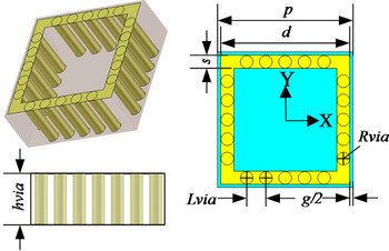
The new, compact single-layer UWB FSS proposed in this study is shown in Fig. 1. The basic unit contains a square loop and multiple metallized vias. The designed FSS structure was printed on an FR-4 substrate with a relative dielectric constant of 4.3; the loss tangent is 0.0025 and the thickness is 1.6 mm. p is the length of the cell's sides and s is the width of the square loop. g is the gap between adjacent cells, and Lvia, Rvia, and hvia are the spacing, radius, and length of the metallized holes, respectively. It should be noted that the dimensional accuracy of the design can be achieved by general processing. If the processing level is further improved, the unit size is expected to be further reduced.
Structure of the proposed FSS unit. p = 4.2 mm, s = 0.4 mm, g = 0.2 mm, Lvia = 0.6 mm, Rvia = 0.2 mm, and hvia = 1.6 mm.

FSS simulation and measurement results
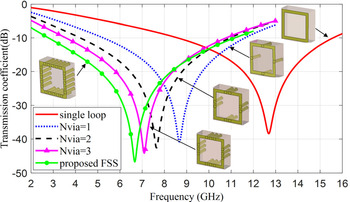
Figure 2 shows the influence of the number of metallized vias on the transmission coefficient of the proposed FSS unit. It can be observed that when there is signal loop structure, the resonant frequency of the FSS is 12.69 GH, and the corresponding −10 dB BW is 8.6–15.6 GHz (BW = 7 GHz). When the number of metallized vias Nvia is 1, the FSS response frequency decreases from 12.69 GHz to 8.67 GHz. As the number of metallized vias increases, the resonance frequency gradually decreases. After all the metallized vias are added, i.e. Nvia = 5, the response frequency of the proposed FSS is 6.67 GHz and the corresponding −10 dB BW is 2.8–11.2 GHz (BW = 8.4 GHz). This result indicates that the FSS response frequency is reduced and the operating BW is widened due to the introduction of metalized vias, which increases the equivalent inductance and capacitance. The corresponding value is related to the radius, length, quantity, and spacing of the adjacent metallized vias.
Influence of the number of metallized vias on the transmission coefficient.

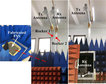
In order to verify the simulation results, the FSS was processed and measured, as shown in Fig. 3. The sample uses 80 × 80 units and has a total size of 336 mm × 336 mm. Rocker 1, rocker 2, transmitting and receiving antenna are used for reflection coefficient measurement. Rocker 1 and rocker 3 cooperate with transmitting and receiving antenna and are used for transmission coefficient measurement. The 3671E vector network analyzer (China Electronics Technology Instruments Limited Company, Qingdao, 370211, China) provided excitation sources and data records.
Fabricated UWB FSS and test environment.

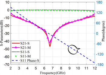
Figure 4 show that the measured results are in good agreement with the simulated results. It can be observed that the FSS has a high attenuation response in the entire frequency range of 3–11 GHz and the reflection phase changes linearly with frequency. When the distance between the antenna and the reflector is $n\lambda /2 ( n = 1, \;2, \;3, \;\ldots ) , \;$ that is, when the co-reflection condition is met, the EM waves reflected by the reflector and the radiated EM waves of the antenna are superimposed in phase to achieve radiation enhancement. The phase of the FSS changes linearly with frequency throughout the operating frequency band, which provides the possibility of achieving broadband radiation enhancement. The transverse electric (TE) and transverse magnetic (TM) modes have the same characteristics at a normal incidence.
Simulated and measured results of the proposed FSS.

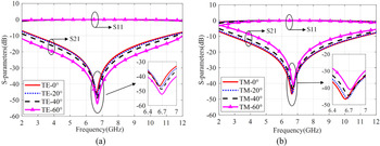
Angle and polarization-independence are also considerations for the design of periodic structures, which are considerably important in UWB systems. Figure 5 shows the S-parameters of the proposed FSS under different polarization modes and incident angles at 2–12 GHz.
S-parameters of the FSS at different incident angles: (a) TE mode, (b) TM mode.

As can be observed from Fig. 5, the FSS has excellent broadband stop-band characteristics in two fundamental modes. In the TE mode (Fig. 5(a)), the resonant frequency is 6.69 GHz at an incident angle of 60°, which is only 0.3% offset relative to the normal incidence. At the same time, in the TM mode (Fig. 5(b)), the resonant frequency is 6.72 GHz and the offset is 0.7%. Thus, the proposed FSS structure has excellent angle and polarization-independence. Similar to the typical characteristics of the conductive element FSS, the resonant BW of the proposed FSS structure in the TE mode widens with an increasing incidence angle; on the other hand, it tends to decrease in the TM mode.
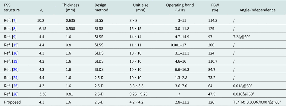
Table 1 compares the size, operating BW, and the angle-independence performance of the proposed FSS with other methods in published literature. In comparison to single-layer single-sided (SLSS) designs [Reference Yahya, Nakamura, Itami and Denidni7–Reference Priyanka and Kaushik9, Reference Kundu15] and single-layer double-face (SLDS) designs [Reference Sayi and Ramprabhu16, Reference Majidzadeh, Ghobadi and Nourinia19,Reference Bashiri, Ghobadi, Nourinia and Majidzadeh20], the structure designed in this study has an advantage in terms of size while ensuring an excellent fractional BW (FBW) performance. Compared with the 2.5-D FSS structure in [Reference Hussain, Cao, Kayani and Majid24–Reference Varikuntla and Singaravelu26], the unit size of the proposed design is 4.2 mm × 4.2 mm, which provides 126% FBW. The resonance frequency under the TE polarization shifts by only 0.003 f 0 at an incident angle of 60°, while the TM polarization shifts by 0.007 f 0. Therefore, the structure proposed in this study is simple and compact, easy to debug and process; it has a large FBW and excellent angle and polarization independence.
Comparison of the proposed design with other FSS designs

Equivalent circuit model
The EC model combines closed equations while providing a simple and efficient means for the initial design and performance estimation of the FSS. The EC model corresponding to the EM simulation model is composed of multiple lumped components. The degree of fineness determines the accuracy of the calculation results; however, this reduces efficiency. Therefore, when the designed model is very complex, the accuracy and efficiency of this method are not satisfactory.
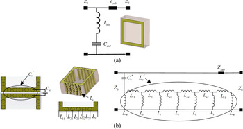
The basic unit in this study contains a square loop and multiple metallized vias. The loop unit can be equivalent to the LC series circuit [Reference Hussain, Cao, Kayani and Majid24, Reference Langley and Parker27]. Figure 6(a) shows the EC of a single loop, where Lout is the inductance of the metal patch and Cout is the capacitance between the adjacent metal patches. Cout and Lout can be calculated according to equations (1) and (2) [Reference Langley and Parker27], where θ is the incident angle of EM waves and s, d, p, and g are the structural parameters in Fig. 1. Because equations (1) and (2) have some limitations, such as p/λ ≪ 1, w/p ≪ 1, and p(1 + sinθ) < 1, the accuracy of the calculation depends on the design parameters.


where


with


Equivalent circuit: (a) signal loop, (b) proposed FSS.

According to equations (1) and (2), Lout and Cout are 2.62 pH and 580.13 nF, respectively.
The capacitance Cv and inductance Lv that are introduced by the via are related to g, Lvia, Rvia, and hvia. The via structure proposed in this study is simple, and the inductance and capacitance can be directly obtained with equations (8) and (9) [Reference Rao28, Reference Savidis and Friedman29].


gvia refers to the spacing of the vias between the adjacent elements, where the value is gvia = g + 2Rvia = 0.6 mm. By applying equations (8) and (9), the capacitance and inductance of the metallized vias can be determined as Lv = 0.616 nH and Cv = 0.199 pF. The total capacitance of the proposed structure is ${C}^{\prime}_v = 5 \times C_v$ .
The inductors L 11 and L 22 can be regarded as metal micro-strip lines in Fig. 6(b), and the inductance value can be obtained according to equations (10) and (11), where b is the thickness of the metal layer, which is usually 0.02 mm. l 1 and l 2 are the lengths of the micro-strip lines corresponding to the L 11 and L 22, and are 0.8 mm and 0.6 mm, respectively.


According to L 11, L 22, Lv, and the EC model shown in Fig. 6(b), the inductance of the proposed structure is equal to ${L}^{\prime}_v$ = 0.443 nH. In addition, the equivalent inductance L e of the virtual cut-off of the periodic structure is equivalent to infinity.
Equation (8) is used to estimate the mutual capacitance of the metallized vias of the two adjacent metal units and the value is closely related to the spacing and length of the via. If the number of metalized vias is large, the dense array of vias on each side is like a metal plate and the capacitance between the neighboring units is similar to the capacitance of parallel metal plates. By applying equation (12), the equivalent capacitance can be approximated as Cp = 1.218 pF. The structural response calculated by the full-wave EM simulation and the EC model is presented in Table 2. It can be observed that the calculation results that use the metal plate capacitor are closer to the EM simulation results.

Comparison of the EM and EC model calculation results

Antenna design
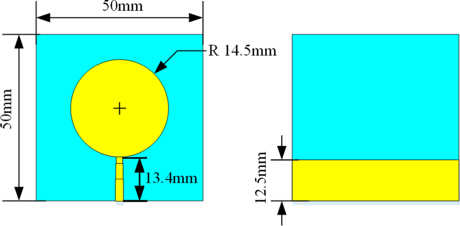
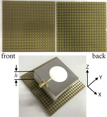
To evaluate the effect of the designed FSS reflector on the UWB antenna port and radiation parameters, a disc monopole antenna was used as the radiator, as shown in Fig. 7. The antenna structure evolved from the monopole antenna in [Reference Liang, Guo, Chiau, Chen and Parini2]. The difference between the antenna used in this study and the one in [Reference Liang, Guo, Chiau, Chen and Parini2] is that the feed mode is changed from co-planar waveguide feed to stepped microstrip feed and the parameters are optimized. The antenna was printed on the Rogers RT5880 substrate with ɛ r = 2.2, tanδ = 0.0009, and a thickness of 1.524 mm. When the feeder length is 2.1, 5.0, and 6.5 mm, the feeder width is 2.0, 2.2, and 2.4 mm, respectively. The FSS reflector is installed directly below the antenna at a distance of h, as shown in Fig. 8.
Structure of the monopole antenna.

Fabricated antenna and FSS reflector.

Antenna loaded proposed FSS
The influence of the reflector on the operating BW and gain of the antenna is closely affected by the distance between the reflector and the antenna. Using the linear relationship between the phase and frequency of the FSS unit, a suitable distance can be determined. In addition, the phase difference can be used to compensate for the wavelength difference. Therefore, the radiated and reflected energy can be superimposed in phase to increase the gain of the antenna within the operating band. The EM wave phase relationship between the FSS reflector and the antenna is given as follows:

where ϕ fss is the phase of the FSS reflection coefficient and β is the free space propagation constant. If ϕ fss = 0, for example, and the corresponding frequency is 7 GHz, h is equal to 21.42 mm; therefore, 22 mm was selected for this study.
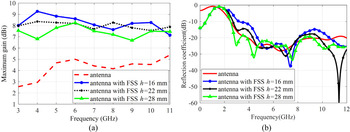
Figure 9 shows the maximum gain and the reflection coefficient of the antenna loaded FSS at different h values. The FSS array that was designed for this investigation uses 20 × 20 units; the overall size of the array is 84 mm × 84 mm.
Effect of the FSS reflector on the antennas at different h values: (a) maximum gain, (b) reflection coefficient.

It can be observed from Fig. 9(a) that the gain of the monopole antenna is about 2.5–5.5 dBi in the 3–11 GHz band and the flatness within the band is poor. The closer the distance, the more evident the effect of FSS reflector is on antenna gain enhancement. In addition, because the antennas have different radiation fields at different frequencies, the amplitude of the antenna gain enhancement at the same distance is also different. The monopole antenna has a relatively large back lobe at low frequencies. After the FSS reflector is loaded, the energy of the back lobe is effectively reflected, which greatly enhances the forward radiation; thus, the antenna has an obvious gain enhancement effect. The main radiation of the monopole antenna in the high-frequency band tends to be parallel to the radiating surface and the radiation of the rear lobe is weak. After the FSS reflector is loaded, the gain enhancement effect is not as evident as in the low-frequency band.
It can be observed from Fig. 9(b) that the reflection coefficient of a monopole antenna is substantially <−20 dB in the entire UWB frequency band. When h = 16 mm, the reflection coefficient of the antenna is significantly worse at 3–4.7 GHz and 9–10 GHz, which is about 5 dB or more. This is mainly because the antenna has a strong backward radiation field at low frequencies and the loading of the FSS reflector has a great influence on the EM field distribution. As the distance increases, this effect gradually decreases. When h = 28 mm, the antenna with and without the FSS has a similar reflection performance for the entire UWB band.
Using the reflection coefficient, gain enhancement, and the in-band gain flatness as the evaluation criteria, it is determined that h = 22 mm is an appropriate choice. This value is consistent with equation (13). After the FSS reflector is loaded, the average gain is 8 dBi, the gain variation is <0.5 dB, and the reflection coefficient is <−15 dB over 3–11 GHz.
Experimental results
The designed antenna and FSS reflector are processed by using common electronic printing techniques. In order to avoid substrate deformation and to fix the distance during the test, the antenna and reflector are supported by a relatively rigid foam (EM parameters are almost equal to air). The SMA-K type connector is attached to the antenna feeding end and the test samples are connected to the test system through a high-frequency coaxial cable.
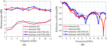
Figure 10 shows the simulated and measured gain and port parameters results for the antenna with and without the FSS reflector when h = 22 mm. It can be observed from Fig. 10(a) that, due to the effect of the FSS reflector, the antenna gain increases by 5.4 dB (3 GHz) and 2.5 dB (11 GHz) at the maximum and minimum, respectively. The gain of the monopole antenna in the UWB band is about 2.5–5.5 dBi, with a gain variation of 3 dB. After loading the FSS reflector, the antenna gain increases to 7.5–8.5 dBi, with a gain variation of only 1 dB, achieving UWB quasi-constant gain enhancement. It can be observed from Fig. 10(b) that the reflection coefficient is lower than the general industry standard of −10 dB in the 3–11 GHz band. In addition, the loading of the FSS reflector does not have a significant influence on the reflection coefficient. Due to the influence of processing and measurement errors, and a difference in the substrate dielectric parameters, there is a certain deviation between the measurement and simulation results; however, it can be determined that the two are in good agreement.
Simulated and measured results for the antenna with and without the FSS reflector. (a) Maximum gain, (b) reflection coefficient.

Table 3 compares the proposed FSS with the previous single-layer UWB FSS in terms of size, BW, and antenna performance. Combining the results shown in Fig. 10(a) and Table 3, it can be determined that the proposed FSS reflector has a clear overall advantage in antenna working BW, antenna quasi-constant gain enhancement and size.
Comparison of the proposed FSS reflector with previous results

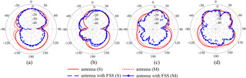
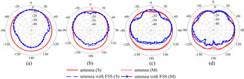
Figures 11 and 12 show the radiation patterns of the antenna in the yz- and xz-plane, respectively. Comparing the results, the improvement effect of the proposed FSS reflector on the radiation characteristics of the UWB antennas is verified. After the antenna is loaded with the FSS reflector, the main lobe is narrowed or the back lobe is made smaller or both, which indicates that the FSS reflector has a significant gain enhancement effect. The results obtained through the measurement are consistent with the simulation. As the influence of the radio frequency connector was not considered in the simulation, it can be observed from Fig. 11 that the agreement between the measurement and the simulation results in the 0°–90° range is better than in the −90° to 0° range. In addition, material differences, machining errors, and measurement errors can also contribute to the deviation of the measurement results.
Radiation patterns of the antenna in the E-plane (yz-plane): (a) 3 GHz, (b) 5 GHz, (c) 7 GHz, and (d) 10 GHz.

Radiation patterns of the antenna in the H-plane (xz-plane): (a) 3 GHz, (b) 5 GHz, (c) 7 GHz, and (d) 10 GHz.

Conclusion
In this study, a miniaturized single-layer UWB FSS design method is proposed. The proposed unit structure has a simple structure (a square loop and metallized vias), a small size (4.2 mm × 4.2 mm, less than one-twentieth of the maximum operating wavelength), excellent angle and polarization independence, and UWB reflection and linear phase attenuation characteristics. As the reflector for a UWB antenna, the proposed structure improves the gain of the antenna and obtains an excellent gain flatness (<0.5 dB). Finally, the measurement and simulation results were compared to prove the feasibility of this design method. This design only involves the application of metalized vias in the FSS miniaturized design. In addition, the miniaturization of antennas, such as branch loading, irregular patterns, and fractal design, could also be combined with 2.5-D structures to obtain an unexpected result, which will also be investigated in future work.
Acknowledgement
This work was partially supported by the Science and Technology on High Power Microwave Laboratory and the Key Research and Development Plan of Shaanxi Province (2017ZDXM-GY-117).
 Yanning Yuan received her B.S. in Electronic Information from Liaoning Shihua University, Fushun, China in 2004 and her M.S. in Communicating Engineering from Xi'an University of Technology, Xi'an, China in 2007. She subsequently joined the Shaanxi Lingyun Science and Technology Co., Ltd. and served as a project manager. She is currently a full-time researcher at Xi'an University of Technology, Xi'an, China. Her research interests include ultra-wideband antennas, multi-frequency antennas, and RF circuits.
 Yuchen Zhao received his B.S., M.S., and Ph.D. degrees in Electronic Science and Technology from Northwestern Polytechnical University, Xi'an, China in 2007, 2010, and 2014, respectively. He joined the faculty at the Electronic Engineering Department, Xi'an University of Technology in 2014. His research interests include wave propagation, photoelectric devices, and microwave integrated circuits.
 Xiaoli Xi received her B.S. in Applied Physics from the University of Defense Technology in Changsha, China in 1990, her M.S. in Biomedical Engineering from the Fourth Military Medical University in Xi'an, China in 1998, and her Ph.D. degree in Electrical Engineering from the Xi'an Jiaotong University in Xi'an, China in 2004. She is currently a Professor at the Department of Electrical Engineering at the Xi'an University of Technology, Xi'an, China. Her recent research interests include antenna design, radio wave propagation and advanced navigation, and electromagnetic technology.