I. INTRODUCTION
The structural order of conjugated polymers and organic molecules, in terms of conformation, aggregation/crystallization, and spatial organization, has a tremendous impact on charge transport properties in organic semiconductor devices.Reference Friederich, Meded, Poschlad, Neumann, Rodin, Stehr, Symalla, Danilov, Ludemann, Fink, Kondov, von Wrochem and Wenzel1–Reference Bassler, Kohler and Metzger3 As a consequence, the film deposition method itself may introduce strong anisotropies in semiconductor organization and thus alongside with that charge transport may exhibit a high orientational dependency. Controlling factors of the molecular organization during the film formation process are OSC material properties (e.g., M N, M W, and PDI for polymers), choice of solvent and solution concentration, preconditioning in solution, and deposition method, as well as processing temperature and atmosphere during deposition. Thus various properties such as molecular aggregation and crystallinity, as well as anisotropy can be fine-tuned by balancing cohesion and adhesion forces.Reference Nguyen, Hoppe, Erb, Günes, Gobsch and Sariciftci4–Reference Zhokhavets, Gobsch, Hoppe and Sariciftci7
While it is known that the charge carrier density may play a crucial role in charge carrier mobility,Reference Tanase, Meijer, Blom and De Leeuw8 and thus highest mobility can generally be obtained for lateral geometry in organic field-effect transistors by making use of mobility anisotropy,Reference Crossland, Tremel, Fischer, Rahimi, Reiter, Steiner and Ludwigs9 the function of organic solar cells essentially depends on the vertical charge transport capabilities. Hence, evaluating the charge carrier mobility of OSCs for use in organic solar cells requires the application of time-of-flight, charge-extraction-by-linearly-increasing-voltage, or space-charge-limited-current (SCLC) methods. The advantage of the latter approach allows investigation of film thicknesses of close to those commonly used in organic photovoltaic devices.Reference Mozer, Sariciftci, Pivrikas, Österbacka, Juška, Brassat and Bässler10–Reference Kastner, Xuechen, Egbe, Ade and Hoppe12
Furthermore, not only the processing of organic solar cells may require the application of thermal annealing steps but also an investigation of photoactive layer stability involves the use of increasing thermal stress recently.Reference Diacon, Derue, Lecourtier, Dautel, Wantz and Hudhomme13,Reference Harnonnet, Nakano, Nakano, Sugino, Takimiya and Tajima14 As a long-term, smaller thermal stress may accumulate to a correspondingly shorter but higher thermal stress; the photovoltaic layer stack should not limit the thermal stability of such devices itself. Ultimately, the charge carrier mobility (µ) of semicrystalline semiconductors such as P3HT can be optimized by melt-crystallizationReference Singh, Gupta, Lohwasser, Engmann, Balko, Thelakkat, Thurn-Albrecht and Hoppe15 or a combination of melt-crystallization and orientation of P3HT-backbones vertically to the substrate.Reference Boulanger, Yu and Barbero16–Reference Skrypnychuk, Boulanger, Yu, Hilke, Toney and Barbero20 Thus, the quest for thermally stable layer stacks and charge extraction layers gained importance for further developing OPV stability and the search for performance limitations. In this contribution, we focused on the thermal stability of the hole extraction layer–electrode combination. By application of single-carrier hole-only SCLC diode devices, superior stability of molybdenum oxide (MoO3)/gold (Au) is demonstrated, which is sufficient to evaluate melt crystallization of the semicrystalline polymer P3HT. It should be noted that the test is performed in the injection mode. However, superior injection as required for obtaining the space-charge-limit is requiring ohmic contacts and thus as well efficient extraction of charge carriers across the same electrode can be concluded.
II. EXPERIMENTAL
The nominal energy levels according to the literature of the materials used in this study, and an exemplary SCLC device architecture and the chemical structure of P3HT are shown in Figs. 1(a)–1(c), respectively. The P3HT batch (P200) used in this study was purchased from BASF. The polymer was dissolved in chlorobenzene yielding solutions of 2 wt% (20 mg/mL). The solutions were prepared and stored in the glovebox under a nitrogen atmosphere at 50 °C and continuously stirred at 600 rpm for at least two weeks.
Energy level diagram of the materials are used in the studiesReference Synooka, Kretschmer, Hager, Himmerlich, Krischok, Gehrig, Laquai, Schubert, Gobsch and Hoppe21,Reference Guo and Robertson22 (a), an exemplary SCLC device architecture (b), and the chemical formula of regio-regular P3HT (c) are depicted.

The hole transport layers (HTLs) used in this study were either poly(3,4-ethylenedioxythiophene)-poly(styrene sulfonate) (PEDOT:PSS) (formulation Heraeus Clevios PH) or MoO3, both in contact with gold electrodes. PEDOT:PSS (was modified by the addition of 10 vol% Isopropanol) and the formulation was spin cast in all cases outside of the glovebox at 3000 rpm, no matter at which side it was used. PEDOT:PSS films were always annealed at 178 °C for 15 min for drying. In the case where PEDOT:PSS was applied on top of the P3HT layers, this already yielded some annealing of the P3HT layer. MoO3 and gold were deposited by physical vapor deposition within a glovebox-attached MiniSpectros from Kurt J. Lesker (Jefferson Hills, Pennsylvania). All films, layer stacks, and complete devices were processed on top of float glass.
A. Film, layer stack, and hole-only SCLC device preparation
Single-carrier hole-only SCLC devices were prepared on glass substrates, yielding a device area of 4 mm2 via the definition of gold electrode overlap. Two different sets of devices were realized: asymmetric devices, bearing on one of the two sides only gold as an injection or extracting electrode, and symmetric devices, were on both sides either PEDOT:PSS or MoO3 was used as a modification of the gold electrodes. The sample preparation consisted of substrate cleaning and deposition of gold, HTLs (MoO3 and PEDOT:PSS) and P3HT active layer on the substrates. Bare glass substrates were subsequently cleaned with acetone and isopropanol in an ultrasonic bath and dried via N2 gun. 100 nm of Au was thermally evaporated on cleaned substrates under high vacuum conditions from tungsten boat; the evaporation rate was 20 A/s. The electrode structure was defined by the shadow mask that was used for the evaporation. After that, either no HTL, 30 nm of PEDOT:PSS or 15 nm MoO3 were deposited by either spin coating or thermal evaporation (physical vapor deposition) through a shadow mask, respectively. The evaporation rate for MoO3 was 8 A/s. Then a ∼300 nm thick layer of P3HT was spin cast on top; the spin coating process was performed inside the glovebox. Finally, either no HTL, PEDOT:PSS or MoO3 was deposited over the P3HT active layer, or yielding either asymmetric or symmetric devices. Devices were completed with the thermal evaporation of the gold top electrode through shadow mask exactitude an active area of 0.04 cm2. SCLC devices were subjected to thermal annealing between 150 and 250 °C with 50 °C increments for 10 min. To protect the completed devices from environmental conditions, the samples were encapsulated using glass and an UV-curing epoxy resin under an inert environment. An exemplary layer stack of the device is depicted in Fig. 1(b).
B. SCLC device characterization
The SCLC devices were characterized in the dark at room temperature with a computer-controlled Keithley 2400 source measure unit (Keithley Instruments, Solon, Ohio). Dark I–V data were recorded from −8 to +8 V. To evaluate the charge carrier mobility, the I–V curves were fitted by using the Murgatroyd SCLC formula for the mobility (µh) determination.Reference Murgatroyd23 Thereby a slight variation of the built-in voltage (V bi) was allowed and evaluated via best fit. The series resistances of specific electrode structures were determined from the respective reference devices fabricated without the active layer.
C. Atomic force microscopy
Film topography was characterized with a Veeco/Bruker Dimension atomic force microscopy (AFM; Veeco Instrument Co., Bruker, Plainview, New York) in the tapping mode, to gain further insight into possible changes of charge transport layers, using super sharp tips (TESP-SS). The images were analyzed by Nanoscope v720 software (Bruker, Karlsruhe, Germany). For AFM measurements, either PEDOT:PSS or MoO3 on gold were investigated.
D. Kelvin probe
To detect a possible change in work function of the layers upon annealing, a single point Kelvin probe (KP) system from Anfatec was used. The probe head dimension was 1.4 mm2. For calibration of the system, freshly cleaved highly oriented pyrolytic graphite was used, and work functions were calculated based on the difference measured.
III. RESULTS AND DISCUSSION
In SCLC devices, the current–voltage (I–V) characteristics are controlled by two fundamental processes: first, injection of charge carriers from the electrodes into the active layer and extraction from the same into the second electrode, second, charge transport in the bulk of the active layer. Thus, the current is either injection (ILC) or bulk limited via built-up of a space charge region. The latter condition is desired in SCLC devices, to determine the charge carrier mobility within the OSC, in this case, P3HT, which was subjected to various annealing conditions. Thus, it is mandatory to have optimized ohmic contacts to ensure that injection is not limiting and hence the electrode-HTL combinations are yielding the highest overall current densities and associated with the hole mobilities also depict optimal interfacial contacts in case of solar cells.
Since OSCs are intrinsically disordered, charge carriers transport happens under the presence of potential barriers causes electric field dependence on charge carrier mobility. This generally is determined by the Poole–Frenkel mobility determination model  $\mu = {\mu _0}{\rm{exp}}\left( {\gamma \sqrt E } \right)$, where µ0 represents the zero electric field and γ is the electric field enhancement factor.
Thus current–voltage (I–V) measurements have been performed to determine the best choice of HTL. Governed by conductivity via intrinsic charge carriers (e.g., due to doping), the I–V characteristics are mostly linear at low bias voltages and become superliner at higher voltages. In case of trap-free charge transport, the slope of the curve at higher voltage becomes 2, according to the Child’s law. In smaller deviations, these exponents are possible due to electric field enhancements, as described by the Poole–Frenkel model. Taking this effect into account leads to the application of the Murgatroyd SCLC formula:
 $$J = {9 / 8}\varepsilon {\varepsilon _0}{\mu _{\rm{h}}}\exp \left( {0.89\gamma \sqrt F } \right){V^2}{L^{ - 3}}\quad ,$$
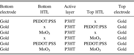
where J is the hole current density, µh is the zero field mobility of holes, ε is the relative permittivity of the material (3.5), ε0 is the permittivity of the vacuum, γ is the field activation factor, L is the thickness of the active layer, and F = V/L is the average electric field across the device. The SCLC hole mobility (µh) of P3HT was determined on devices annealed under different temperatures. Table I summarizes the variation in the bottom and top HTLs of the different SCLC devices realized.
Overview of the experimental variation of HTLs.

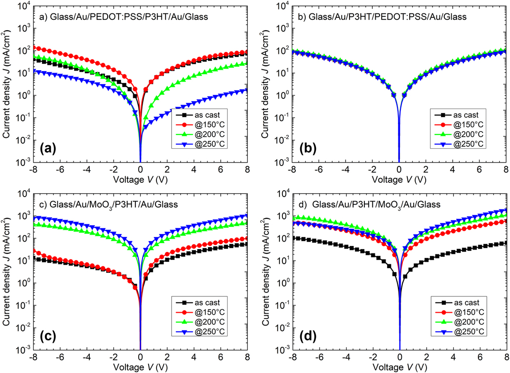
Figure 2 depicts the J–V characteristics of the devices with asymmetric contact materials from as-cast up to annealing temperatures of 250 °C. Most devices actually exhibit asymmetric characteristics, when comparing the forward and reverse currents. Only in case of the Au/P3HT/PEDOT:PSS/Au devices, all curves fall on top of each other and show symmetric behavior with respect to the sign of voltage applied.
Diode-characteristics of asymmetric SCLC devices recorded at room temperature and plotted on a semilogarithmic scale. (a) Glass/Au/PEDOT:PSS/P3HT/Au/glass, (b) glass/Au/P3HT/PEDOT:PSS/Au/glass, (c) glass/Au/MoO3/P3HT/Au/glass, and (d) glass/Au/P3HT/MoO3/Au/glass.

As devices exhibiting MoO3 HTLs demonstrated already higher current densities, the deviation is not likely to stem from bulk charge transport. Thus all asymmetric devices displaying PEDOT:PSS on either side of the P3HT active layer do not seem to show the actual hole mobility and must be injection limited. However, it remains not fully understood why forward/reverse currents of the Au/PEDOT:PSS/P3HT/Au device does not reproduce the reverse/forward currents of the Au/P3HT/PEDOT:PSS/Au device. At this point, it can only be concluded that the interfacial property of the PEDOT:PSS injection layer depends on the order of processing, or in other words, PEDOT:PSS exhibits a different interfacial organization when processed on top instead of below the P3HT layer. This can be in part comprehended, as it has been shown earlier that commonly the PSS groups are enriched at the surface of any PEDOT:PSS layer and furthermore facilitate improved injection via interfacial dopingReference Herrmann, Muhsin, Singh, Shokhovets, Gobsch, Hoppe and Presselt24 and also interface dipoles are possible.
The presence of PSS at the interface may further explain the degradation of injection properties for temperatures above 150 °C for the Au/PEDOT:PSS/P3HT/Au layer stack. As already stated, devices containing one MoO3 HTL presented improved injection properties. However, the pristine gold electrode on respectively one of the two sides seems to have limited injection yields, leading to the slightly asymmetric shape with respect to the sign of voltage bias. This observation already rules out bare gold contacts on both sides to be optimal.
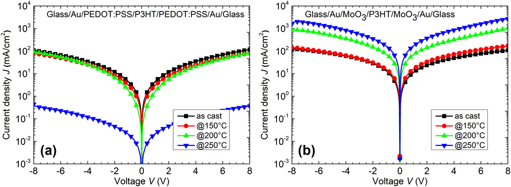
Next, the results obtained from symmetric devices are presented. Figures 3(a) and 3(b) display the current–density (J–V) voltage characteristics of symmetric PEDOT:PSS and symmetric MoO3 single carrier hole only device. In the case of symmetric PEDOT:PSS devices, charge carrier mobilities are independent of annealing temperature up to 200 °C in forward and reverse regimes. However, the device degraded drastically under thermal annealing at 250 °C and current densities (J) reduced by two orders of magnitude. Here, the devices are dominated by degradation of injection properties. It can be noticed from the J–V characteristics that all the devices exhibit a symmetric behavior when the symmetric hole transport materials are used on both sides. This observation is kind of interesting, as specifically for the asymmetric device exhibiting the Au/P3HT/PEDOT:PSS/Au layer stack, no degradation of current density was observed at 250 °C.
Diode characteristics of symmetric SCLC devices recorded at room temperature and plotted on a semilogarithmic scale. (a) Glass/Au/PEDOT:PSS/P3HT/PEDOT:PSS/Au/glass and (b) glass/Au/MoO3/P3HT/MoO3/Au/glass.

By contrast, the symmetric devices using MoO3 as HTLs exhibit nicely symmetric J–V characteristics. On top of that, a consistent increase of current densities is observed for annealing temperatures above 150 °C, reflecting increased hole mobility due to the improved ordering of the P3HT.Reference Singh, Gupta, Lohwasser, Engmann, Balko, Thelakkat, Thurn-Albrecht and Hoppe15
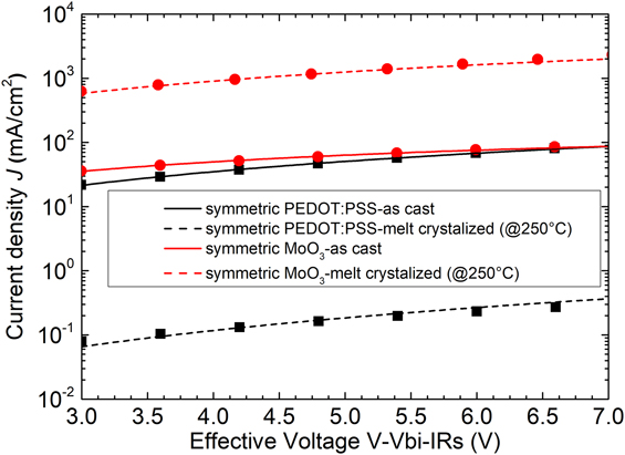
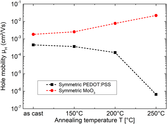
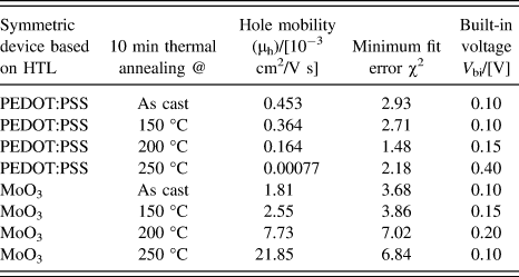
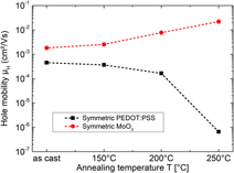
The dark J–V curves were fitted with the above-stated Murgatroyd formula [Eq. (1)]. Such SCLC fits for as-cast and melt-crystalized symmetric devices are shown in Fig. 4. Calculated charge carrier mobilities for devices annealed at various temperatures are shown in Fig. 5 and summarized along with the fit-error and the determined built-in voltage in Table II. Although the two interfacial contacts are made from the same electrode, an energy offset of the symmetric devices was found from 100–400 mV, ascribed to differences in the interface between the bottom and top interface. This was essential to correctly interpret the shape of the current–voltage characteristics at low voltage.Reference Dacuña25 While for devices using MoO3, a consistent increase in hole mobility is found, and PEDOT:PSS as HTLs yields the complete opposite behavior. This finding rules PEDOT:PSS out for reliable investigation of thermally treated devices above 150 °C.
SCLC fits using Murgatroyd formula and the J–V characteristics were corrected for the built-in voltage (V bi) and the voltage drop over the contacts.

SCLC hole mobilities obtained from symmetric devices subjected to no (as cast) and annealing at elevated temperatures up to 250 °C. The mobility values were determined by fitting the J–V characteristics according to Eq. (1).

Extracted SCLC hole mobilities obtained from symmetric devices subjected to different thermal annealing conditions up to 250 °C. The mobility values were determined from SCLC fits, and a minimum fitting error occurred for the respective built-in voltage [V bi] reported.

It is interesting to mention here that the derived SCLC-mobility of 0.022 cm2/V s for the melt-crystallized P3HT annealed at 250 °C using MoO3 as HTL displays, to the best of our knowledge, the highest value reported in the literature for vertical charge transport in P3HT-diodes to date. In other recent studies on disrupted P3HT-films, micropatterning was used to yield vertically oriented P3HT-backbones, and with those even higher vertical charge carrier mobilities of up to ∼10 cm2/V s have been reported.Reference Ro, Akgun, O’Connor, Hammond, Kline, Snyder, Satija, Ayzner, Toney, Soles and DeLongchamp26–Reference Baeg, Khim, Kim, Koo, You, Choi and Noh29 The authors showed that those values could be understood as close to the limit since maximum hole mobility values obtained via probing the charge transport only locally by Terahertz spectroscopyReference Cunningham and Hayden30 yielded one order of magnitude higher mobilities (30–40 cm2/V s), which coincides with theoretical calculations.Reference Skrypnychuk, Wetzelaer, Gordiichuk, Mannsfeld, Herrmann, Toney and Barbero27,Reference Northrup31
In view of that, the herein reported mobility values thus correspond to about one-thousandth of the maximum hole mobility in well-ordered P3HT chains along with the backbone. However, our case transport is dominantly following side-chain or π–π stacking direction—in agreement with structural investigations, that either report edge-on or face-on orientation of P3HT crystallites.Reference Kline, McGehee, Kadnikova, Liu, Frechet and Toney32–Reference Balko, Portale, Lohwasser, Thelakkat and Thurn-Albrecht34 And in either case, this corresponds to a parallel organization of the P3HT-backbones for spin-cast or drop-cast films.Reference Zhokhavets, Erb, Hoppe, Gobsch and Serdar Sariciftci5,Reference Zhokhavets, Gobsch, Hoppe and Sariciftci6
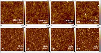
To gain deeper insight into possible morphology changes of the HTLs upon annealing, AFM measurements were performed on these HTLs coated on Au electrodes and are shown in Fig. 6. The first observation upon annealing of PEDOT:PSS and MoO3 films under the same conditions is that there are no dramatic changes. However, there are minor changes observed for the stacks annealed at high temperature. It seems that upon annealing at the most elevated temperature, PEDOT:PSS films develop slightly higher crystallinity, indicated by somewhat increased surface roughness and better visibility of small grainy structures. No apparent changes were observed in case of MoO3, the apparent increase in grain size should be related to a degradation of the AFM tip itself.
AFM topography images (2 × 2 µm) showing PEDOT:PSS and MoO3 films on Au, which have been annealed at 150, 200, and 250 °C. As-cast films are shown as a reference as well. In general, no much change is observed. Upper row: PEDOT:PSS films annealed at (a) as-cast, (b)150 °C, (c) 200 °C, and (d) 250 °C, lower row: MoO3 films annealed at (e) as-cast, (f) 150 °C, (g) 200 °C, and (h) 250 °C, respectively.

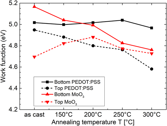
To shed further light on possible energetic changes of PEDOT:PSS and MoO3 films upon annealing, their work function was investigated by KP method, and the results are shown in Fig. 7. For that, four different layer stacks were investigated: (i) glass/gold/PEDOT:PSS (Bottom PEDOT:PSS), (ii) glass/gold/PEDOT:PSS/P3HT/PEDOT:PSS (Top PEDOT:PSS), (iii) glass/gold/MoO3 (Bottom MoO3), and (iv) glass/gold/MoO3/P3HT/MoO3 (Top MoO3). Interestingly, the bottom PEDOT:PSS films exhibited almost no variation concerning the work function, while the top PEDOT:PSS films showed a constant drop from close to 5 eV down to about 4.6 eV. More surprisingly, also the bottom MoO3 exhibited a strong reduction upon annealing from close to 5.2 eV down to slightly below 4.8 eV. However, the top MoO3 films exhibited the most irregular behavior, initially raised upon annealing from 4.7 eV to about 4.9 eV at 200 °C, then the work function decreased again for temperatures up to the maximum investigated here (300 °C). It should be noted here that even though annealing was performed under inert conditions in a glovebox, the KP characterization was performed under air. However, this cannot be the reason for the observed variations in work function. While the work function of PEDOT:PSS depends on the ratio between PSS and PEDOT at the surface,Reference Synooka, Kretschmer, Hager, Himmerlich, Krischok, Gehrig, Laquai, Schubert, Gobsch and Hoppe21,Reference Nau, Schulte, Winkler, Frisch, Vollmer, Koch, Sax and List35 not much is known concerning MoO3. However, the work function of evaporated MoO3 decreases after exposure to air due to a very thin layer of oxygen-rich adsorbate on the MoO3 film.Reference Irfan, James Turinske, Bao and Gao36,Reference Schulz, Tiepelt, Christians, Levine, Edri, Sanehira, Hodes, Cahen and Kahn37 The work function of MoO3 can generally be recovered with increasing annealing temperature in vacuum.Reference Irfan, James Turinske, Bao and Gao36
Work function of bottom and top HTLs (PEDOT:PSS and MoO3).

It is furthermore clear that the work function for top HTL devices is not the one acting towards the interface to the P3HT layer below. One favorable fact may be that the work function for MoO3 becomes similar for higher annealing temperatures. However, to understand the full effects, it should be taken into consideration that MoO3 is known to dope OSCs which results in barrier-free hole injection. Finally, it should be noted that the experimental observation that symmetric single-carrier hole-only devices based on MoO3 as HTL seem to offer a stable condition concerning favorable contact formation with minimized injection (and thus also extraction) barriers for hole transfer between the electrode and OSCs—here P3HT.
IV. CONCLUSION
With increasing importance of thermal annealing steps—either during semiconductor processing or for testing thermal stability of complete devices based on OSCs such as organic solar cells—the design of stable performing electrodes in combination with charge transport layers becomes essential. Here, we demonstrated that MoO3 as the HTL could fulfill the expectations for high-temperature stable charge injection and extraction properties. Even though gold was used in this study for the electrodes, also other metals should be yielded stable features, as long as oxidation does not harm contact resistances.
In summary, we presented with gold/MoO3, a metal electrode/hole transport material combination that can sustain its favorable properties up to annealing temperatures of 250 °C, enabling the study of mobility changes upon melt crystallization of somewhat crystalline regio-regular P3HT. To the best of our knowledge, the obtained vertical hole mobility of 0.022 cm2/V s displays the highest value ever reported to date for pristine P3HT films. It is expected that also other more recent representatives of semicrystalline OSCs can be investigated with respect to their vertical charge transport potential upon melt crystallization.
ACKNOWLEDGMENTS
SA and HH are grateful for financial support from Deutsche Forschungsgemeinschaft (DFG) in the frame of “PhotoGenOrder” project. The authors appreciate for the AFM measurements supported by A. Paszuk at TU-Ilmenau.