I. INTRODUCTION
The miniaturization (or scaling) of switching and data storing elements, such as transistors and capacitors, in semiconductor devices according to Moore’s law has been the major impetus for the continued and very successful growth of the semiconductor industry and various branches of information technology. However, the continuously decreased feature size of the devices is already reaching its practical and physical limitations (∼10 nm), so different strategies are urgently needed. The practical limitations can be summarized by the ever-increasing and already extremely expensive patterning processes required as scaling progresses, while the physical issues arise from the literally countable number of electrons present in transistors at this size scale. When the number of electrons becomes countable quantum mechanical uncertainty can no longer be neglected, and no further scaling can be pursued considering the unavoidable pattern-size variation (typically ∼5% of the feature size). Therefore, two approaches are currently being pursued; one is to integrate the devices in a vertical way, an example being vertical NAND flash memory,Reference Tanaka, Kido, Yahashi, Oomura, Katsumata, Kito, Fukuzumi, Sato, Nagata, Matsuoka, Iwata, Aochi and Nitayama1 which is the more feasible approach for memory devices, and the other is to adopt new functional materials, such as the high-k gate dielectrics in high-performance logic chips.Reference Wilk, Wallace and Anthony2 Of course, these examples do not limit the application of these new approaches since the vertical device, such as fin-type field effect transistors, is also an important research field for logic chips, and new functional materials are crucial for the reliable functioning of various types of new memories that are under development, such as phase change random access memory.
Dynamic random access memory (DRAM) still works as a main memory in every modern high-performance computer and “pad”-type hand held device. This is due to the unrivaled simultaneous realization of supreme performance (speed, endurance, and efficient memory utilization) and ultrahigh density among the various types of memories. However, DRAM has two critical problems; one is its volatile data retention and the other is its incompatibility with vertical integration. The volatile character of DRAM cannot be avoided in principle, although the refresh performance can be improved by implementing transistors with smaller off current and capacitors with lower leakage current levels. The vertical integration of DRAM is extremely difficult due to the presence of capacitors. Therefore, for the given structure of DRAM, the adoption of a new functional material that can assure higher cell capacitance, as reviewed in this article, is the only way by which the DRAM can improve its performance. TiO2 thin films are especially important in this regard.
Resistance switching random access memory (ReRAM) is an emerging new memory that utilizes a new functionality found in nonconventional materials, which uses the bistable and mutistable switchable resistance states of these materials.Reference Sawa3 Although there are several categorizations for this type of memory depending on the resistance switching (RS) mechanism and voltage application direction,Reference Waser, Dittmann, Staikov and Szot4 this article is restricted to only the ReRAM memories based on thermochemical and electronic mechanisms, which is typically shown in TiO2, since only TiO2 thin films are of concern in this article. Interestingly, the RS of TiO2 films is derived from a (softly) broken down state of the capacitor in the metal-insulator-metal (MIM) configuration, which is of the same configuration as that of capacitors in DRAM. Of course, the (softly) broken down state of TiO2 must be avoided in DRAM. The reversible RS in TiO2 can be operated both in unipolar RS (URS), where a single bias polarity is used to switch the sample between the high and low resistance states, and bipolar RS (BRS), where both bias polarities are necessary to induce the switching.Reference Choi, Jeong, Kim, Rohde, Choi, Oh, Kim, Hwang, Szot, Waser, Reichenberg and Tiedke5–Reference Tsunoda, Fukuzumi, Jameson, Wang, Griffin and Nishi7 Another critical merit of ReRAM is its possible integration into high-density matrix type memory using the crossbar architecture where the select transistor can be replaced by a diode.Reference Lee, Seo, Kim, Ahn, Seo, Yoo, Baek, Kim, Byun, Kim, Hwang, Kim, Jeon and Park8 This is a very plausible feature of interest in the context of fabrication of the vertically integrated structure because both the memory cell and select device have the two-terminal configuration, which can be easily stacked on the side-wall area of a vertical memory structure.Reference Baek, Park, Ju, Seong, Ahn, Kim, Yang, Song, Kim, Park, Park, Song, Jeong, Choi, Kang and Chung9
Interestingly enough, the above-mentioned essential features demanded of the prospective new functional materials, that is, high capacitance in DRAM and fluent RS in ReRAM, can be achieved in TiO2. The three-dimensional (3D) structures of DRAM and ReRAM require a film growth technique that offers a high degree of conformality over severely topological and heterogeneous surfaces, which can be achieved from atomic layer deposition (ALD). Therefore, this review article describes the followings; first, the basic material properties of TiO2 are briefly reviewed. Herein, the discussion is limited to the structure of interest for the applications mentioned above; rutile. The structural and chemical features of rutile phase TiO2 is discussed with respect to its crystallographic and quantum mechanical band structures that result in the extraordinarily high value for the dielectric constant for DRAM and structural transitions for ReRAM. Then, the thin film growth processes for TiO2 thin films are briefly reviewed with emphasis on ALD. Since TiO2 is a simple binary oxide, it is fairly easy to grow TiO2 films on various substrates using several thin films deposition processes, such as sputtering, chemical vapor deposition (CVD), and ALD. However, the growth of films with satisfactory performance is rather limited to only certain cases due to the relatively easy formation of defects, which is partly attributed to the relatively small band energy difference between TiO2 and its suboxides compared with other oxides, such as hafnium oxide (HfO2).Reference Yang, Strachan, Miao, Zhang, Pickett, Yi, Ohlberg, Medeiros-Ribeiro and Williams10 The smaller band gap (Eg) of TiO2 (3.1–3.2 eV) compared with others makes it vulnerable to unwanted performance degradation even with lower (point) defect densities. Therefore, ALD is the process of choice for obtaining high-quality TiO2 films. Next, the performance of the TiO2 (or doped TiO2) films in DRAM and ReRAM are discussed in detail, where a summary of recent important reports is provided with some of the authors’ recent improvements. Finally, the article provides the readers with a conclusion and some outlook.
II. THE NONSTOICHIOMETRY OF TiO2
TiO2 is a typical hypostoichiometric compound, in which oxygen is deficient, i.e., TiO2−x. Its hypostoichiometry is known to result from point defect formation. Owing to the positive contribution of point defects to the entropy of TiO2, its nonstoichiometry is indeed inevitable from a thermodynamic point of view. For a long period, there was considerable speculation over the dominant defect type in hypostoichiometric TiO2. Two different types of defects are estimated to possibly lead to the hypostoichiometry, which are titanium interstitialsReference Kofstad11–Reference Meis and Fleche14 and oxygen vacancies.Reference Baumard, Panis and Anthony15–Reference Andersson, Kollberg and Jelenski17 However, the dominant defect type in TiO2 appears to be a matter of thermodynamic conditions in the measurements, mostly temperature. As Marucco et al. demonstrated, at low temperatures, oxygen vacancies are most likely the dominant defect type, whereas, at high temperatures, titanium interstitials prevail.Reference Marucco, Gautron and Lemasson13
In spite of the thermodynamic stability of point defects, i.e., oxygen vacancies, in TiO2, there is a certain upper limit in the concentration of these defects that can be accommodated in TiO2 if its crystal structure is to be sustained.Reference Banus and Reed18 The upper limit of x in TiO2−x is known to be 0.008 at 1000 K.Reference Banus and Reed18 That is, at the most 0.4% of the oxygen ion sites can be empty. When the concentration of oxygen vacancies crosses the upper limit boundary, the phase instability of original TiO2 structure becomes very high and phase-transition leading to a second phase(s) occurs. In the phase diagram of Ti–O compounds, one can find a number of stable phases of Ti–O compounds, for instance, TinO2n−1 phases, where n = 1, 2, 3, …, right beside the TiO2 phases, which are referred to as Magnéli phases.Reference Bursill and Hyde19 The evolution of Magnéli phases is a result of the formation of crystallographic shear planes (CSPs) that result from oxygen vacancy clustering. Note that these extended defects, i.e., CSPs, do not contribute to an increase in the entropy as point defects do.
The effects of point defects on the electrical properties of TiO2 are quite straightforward. Because oxygen vacancies serve as donors in TiO2, an increase in their concentration leads to an increase in the concentration of delocalized electrons, and thus the conductivity of TiO2 is increased under these circumstances. In addition, as demonstrated by Jeong et al., an increase in the concentration of oxygen vacancies perhaps decreases the Schottky barrier height at the metal–TiO2 interface.Reference Jeong, Schroeder and Waser20 Not only direct current (DC) characteristics but also alternating current (AC) characteristics of TiO2 appear to be influenced by oxygen vacancy concentration. In addition to the ionic polarizability of TiO2, the back-to-back double layers formed in a metal–TiO2–metal junction perhaps contribute to the dielectric behavior in a frequency domain, especially, in a low frequency region. The contribution of the double layers is a matter of oxygen vacancy concentration as well as the diffusion coefficient or mobility.
In TiO2, oxygen vacancies play two extremely different roles when the material is used for dielectric and RS functionalities, the two major applications that are of interest in this article. That is, oxygen vacancies in TiO2 as a capacitor dielectric (with low dielectric loss) are very deleterious; so it is very important to reduce oxygen vacancy concentration as low as possible. On the contrary, when TiO2 serves as a RS material, oxygen vacancy formation is of great importance since the formation of conducting filaments made of Ti suboxides, i.e., Magnéli phases, plays a key role in its RS.Reference Kim, Lee, Seok, Song, Yoon, Yoon, Lee, Kim, Lee, Ryu, Park and Hwang21–Reference Strachan, Pickett, Yang, Aloni, David Kilcoyne, Medeiros-Ribeiro and Williams23
III. ALD FOR NEXT-GENERATION MEMORY DEVICES
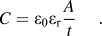
One of most critical challenges which DRAM technology has been confronted with is the achievement of sufficient cell capacitance. For the successful operation of DRAMs, the cell capacitance of DRAM devices should be higher than 25 fF/cell due to the parasitic noise, irrespective of technology node. However, the scaling down of DRAM cells has made cell capacitor size progressively smaller, making it progressively more and more cumbersome to achieve sufficient cell capacitance. The capacitance in a DRAM cell is expressed by the following;
 $$C = {\rm{\varepsilon }}_{\rm{0}} {\rm{\varepsilon }}_{\rm{r}} {A \over t}.$$
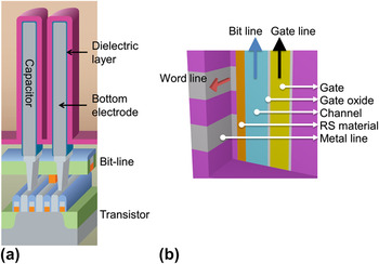
Where C, ε0, εr, A, and t indicate the capacitance, permittivity of vacuum, dielectric constant of the dielectric layer, effective area of capacitor, and film thickness, respectively. 3D structured capacitors such as cylinder type devices have been used to increase the surface area of capacitors as shown in Fig. 1(a).Reference Kim, Lee, Han, Lee, Han and Hwang24 However, the ever-shrinking design rule results in a fragile device due to the weaker mechanical strength in the tall storage nodes. This generally leads to the tilting or even breakage of these storage nodes. Therefore, decreasing storage node height in DRAM cells is inevitable as the design rule scales down further. An alternative would be to decrease dielectric film thickness, but this brings high leakage currents, meaning that it is not a good approach either. Consequently, the only way to achieve sufficient capacitance is to replace the dielectric layer with a higher-k material such as rutile-structured TiO2. The high-k material should also be capable of being grown on the 3D-structured capacitors shown in Fig. 1(a). This requires extremely conformal film growth on the severe 3D structure (aspect ratio of ∼100). ALD is the only method that can achieve excellent conformality on these extreme 3D structures. Therefore, the dielectric film in DRAM capacitors should be grown by ALD.
Schematic diagrams of (a) DRAM cells which consist of a cell transistor and capacitor (reproduced from Ref. Reference Kim, Lee, Han, Lee, Han and Hwang24. Permission acquired from Wiley-VCH) and (b) 3D stacked crossbar device.

ReRAM has recently received great interest as a strong candidate for new memory devices. Up to now, studies concerning ReRAM have focused on the RS phenomena of planar structured cells so far. However, the 3D stacked structure attracts a great deal of attention in the field of nonvolatile memory devices since it can improve the integration density without increasing the fabrication cost to astronomical levels, and research in this area is pending. Figure 1(b) shows one of the schematic structures for the 3D stacked crossbar device proposed by some of the authors.Reference Seok, Kim, Kim, Kim, Chung, Song, Yoon, Yoon, Lee, Kim and Hwang25 The structural modification of the cell would be another key area of research for this type of memory device in the future. This structural modification of ReRAM into 3D stacks requires conformal growth of the RS material as well as other materials, such as metal electrodes. Therefore, it is also obvious that the RS material should be grown by ALD.
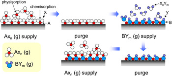
ALD is a timely and promising growth method for high-quality thin films in microelectronics including DRAMs and ReRAMs from this point of view.Reference Leskelä and Ritala26–Reference Kuesters, Beug, Schroeder, Nagel, Bewersdorff, Dallmann, Jakschik, Knoefler, Kudelka, Ludwig, Manger, Mueller and Tilke29 In contrast to conventional CVD where all the reactants are simultaneously injected into a reactor, ALD is based on the sequential introduction of the precursors and reactants. Figure 2 shows the schematic diagram of a typical ALD reaction. The residual reactants and by-products are purged out between the injection steps of each reactant. The growth in each step is self-limited after the chemisorption of the reactants on all the available sites of the reaction surface. This self-limiting mechanism of ALD enables the unique and valuable characteristics of ALD. The growth rate of an ALD process is generally defined as the increment of film thickness per one cycle performed in the reaction chamber. This characteristic allows thickness control to be much easier and more accurate in the subnanometer range. In addition, even at low temperatures, ALD can produce promising quality films with smooth morphology, no pinhole, less impurity, etc., since ALD is not based on the thermal decomposition of precursors but specific surface ligand-exchange reactions. Most importantly, ALD is capable of achieving excellent step coverage even on complex structures with an extremely high aspect ratio (>several hundreds) owing to the self-limiting mechanism.Reference Gordon, Hausmann, Kim and Shepard30 This capability of conformal growth seems to certainly lead to significant improvements in next-generation DRAM and ReRAM devices.
Schematic diagram of ALD reaction.

TiO2 is one of the materials for which the ALD process is well established. The excellent step coverage of ALD TiO2 films can be achieved relatively easily.Reference Kim, Kim, Kwon, Lee, Jeon, Park, Hwang and Jeong31 There are many reports on ALD of TiO2 thin films from various Ti precursors and oxygen sources.Reference Kim, Hwang, Kwon, Kim, Cho, Jeong, Lee, Seo, Hwang, Min and Cho32–Reference Aarik, Aidla, Mändar and Uustare35 However, the details on the ALD reactions of TiO2 films from various reactants are not dealt with in this article. Herein, the properties and performance of ALD-grown TiO2 films for DRAM and ReRAM applications are discussed.
IV. ALD TiO2 THIN FILMS FOR DRAMS
A. Rutile TiO2 films growth by ALD
TiO2 has several polymorphic phases such as anatase, brookite, and rutile. Among the polymorphic structures, rutile-structured TiO2 films have received great interest as a strong candidate for the high-k capacitor dielectric application in the next-generation DRAM capacitors because the rutile-structured TiO2 films have highest values for the dielectric constant (170 along the c-axis and 90 along the a-axis, respectivelyReference Diebold36) among the known binary dielectric oxides. Anatase-structured TiO2 has a much smaller value for dielectric constant (30–40). The high value for dielectric constant of rutile TiO2 comes from the very high born effective charges of the Ti and O ions and the soft optical phonon mode in the crystal structure.Reference Lee, Ghosez and Gonze37
There have been many attempts to control the crystalline phase of TiO2 thin films since the interesting properties of TiO2 are strongly dependent on the crystalline structure. The crystalline phase of TiO2 films grown by ALD (and even CVD) is dependent on the various deposition conditions. Among these, the growth temperature is the most critical factor that determines the crystalline phase of TiO2 films. The Rutile structure of TiO2, which is the high temperature phase, generally requires a high growth temperature (>500 °C) or high annealing temperature (>700 °C). As described above, the stringent requirement of conformal growth over extreme 3D structure in DRAM capacitors can only be satisfied by ALD. However, most conventionally available Ti precursors for the ALD growth of TiO2 thin films decompose thermally at these temperatures (>400 °C), so the ALD growth of rutile phase TiO2 thin films could not be achieved. Most of the TiO2 films grown by ALD have anatase or amorphous phases, which have relatively low value for dielectric constants (<40).Reference Kim, Hwang, Kwon, Kim, Cho, Jeong, Lee, Seo, Hwang, Min and Cho32, Reference Kim, Hoffmann-Eifert, Mi and Waser34 There are only a handful of reports on the growth of rutile TiO2 films by ALD with halide precursors such as titanium tetrachloride (TiCl4) and titanium tetraiodide (TiI4), which can withstand high temperature.Reference Aarik, Aidla, Uustare, Kukli, Sammelselg, Ritala and Leskelä38, Reference Schuisky, Aarik, Kukli, Aidla and Hårsta39 However, the ALD reaction from these halide precursors generates hydrogen chloride (HCl) or hydrogen iodide (HI) as the by-product, which are not compatible with an ALD tool for mass production.
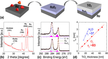
The authors reported the ALD growth of rutile-structured TiO2 thin films on a ruthenium (Ru) substrate at a temperature as low as 250 °C where most Ti precursors can be used for the ALD growth of TiO2 films.Reference Kim, Kim, Kim, Hwang and Jeong40 In the report, interestingly, the rutile-structured TiO2 is formed only on the Ru substrate whereas anatase-structured TiO2 is formed on other substrates such as platinum (Pt) and silica (Si) despite the same deposition conditions.Reference Kim, Kim, Kim, Hwang and Jeong40 The critical factor for the formation of rutile TiO2 on Ru is the presence of interfacial RuO2, which is structurally compatible with rutile TiO2. RuO2 also has a rutile phase, and has a good lattice match with rutile TiO2.Reference Kim, Kim, Kim, Hwang and Jeong40, Reference Kim, Hwang, Kim and Hwang41 As shown in Fig. 3(a), the ALD process from oxygen sources with strong oxidation potentials can form very thin RuO2 layers at the initial growth stage.Reference Kim, Kim, Kim, Hwang and Jeong40 The interfacial RuO2 layer induces the formation of rutile TiO2 due to the structural compatibility in spite of the low growth temperature of 250 °C.Reference Kim, Kim, Kim, Hwang and Jeong40, Reference Kim, Hwang, Kim and Hwang41 Indeed, the ALD process of TiO2 films with H2O resulted in the formation of an anatase phase while the ALD process of TiO2 films with gases with strong oxidation potentials such as ozone (O3), oxygen (O2), or nitrous oxide (N2O) plasma gave rise to the formation of a rutile phase on the Ru electrode as shown in Fig. 3(b).Reference Kim, Hwang, Kwon, Kim, Cho, Jeong, Lee, Seo, Hwang, Min and Cho32, Reference Kim, Kim, Kim, Hwang and Jeong40 This is because the O3, O2-, or N2O plasma formed a thin interfacial RuO2 layer in the initial growth stage, which enables the formation of rutile TiO2. Figure 3(c) shows the Ru 3d x-ray photoelectron spectra of Ru substrates under 1-nm thick TiO2 films grown by H2O and O3, respectively.Reference Kim, Kim, Kim, Hwang and Jeong40 The sample grown with O3 clearly showed a strong signal of RuO2 phase. This supports the premise that the interfacial RuO2 layer induces the formation of rutile TiO2 films in low temperature ALD processes. In addition, fortunately, RuO2 has very low resistivity (∼40 μΩ cm) meaning that the interfacial RuO2 layer does not lead to a loss in the capacitance but simply works as a part of the electrode.
(a) Schematic process flow for the formation of rutile TiO2 on Ru by ALD. (b) Glancing angle XRD patterns of TiO2 films grown with H2O and O3 as the oxygen source, respectively. (c) Ru 3D x-ray photoelectron spectra of Ru substrates under 1-nm thick TiO2 films with H2O and O3, respectively. (d) The variation in the t ox value of TiO2 films as a function of film thickness. (Figure and data reproduced from Ref. Reference Kim, Kim, Kim, Hwang and Jeong40. Permission acquired from the American Institute of Physics.)

The ALD rutile TiO2 films grown on the Ru electrode showed a much higher value for dielectric constant compared with the anatase TiO2 films grown by ALD. Figure 3(d) shows the variation in the equivalent oxide thickness (t ox) of the TiO2 films as a function of film thickness.Reference Kim, Kim, Kim, Hwang and Jeong40 The value for dielectric constant extracted from the inverse slope of the graph is ∼83 for the rutile TiO2 films and ∼37 for anatase TiO2 films, respectively, which is consistent with the crystalline structure. The high value obtained for the dielectric constant of rutile TiO2 films makes ALD TiO2 films a very promising capacitor dielectric for next-generation DRAM capacitors.
It is also important to optimize the exposure time of the oxygen sources such as O3 or O2 plasma to assure good electrical properties in the TiO2/Ru capacitor. The authors reported that a long O3 exposure time (>5 s) in respect of the Ru electrode deteriorated the leakage properties of the TiO2/Ru capacitor.Reference Kim, Lee, Seo, Choi and Hwang42 The long O3 exposure time roughened the interface attributable to the severe nonuniform oxidation of the Ru electrode at the initial growth stage.Reference Kim, Hwang, Kim and Hwang41, Reference Kim, Lee, Seo, Choi and Hwang42 The rough interface largely increased the leakage currents of the TiO2/Ru capacitor. Excessive exposure of Ru electrodes to an O3 environment can also etch away the Ru through a disproportionation reaction (2RuO2 → Ru + RuO4).Reference Green, Gross, Papa, Schnoes and Brasen43
Rutile TiO2 films can be formed on other substrates besides Ru electrode. The authors reported observing rutile TiO2 growth directly on RuO2 electrodes at a growth temperature of 250 °C.Reference Kim, Hwang, Kim and Hwang41, Reference Han, Han, Lee, Lee, Kim, Gatineau, Dussarrat and Hwang44 The rutile TiO2 films are formed on the RuO2 electrodes irrespective of oxygen sources. Fröhlich et al. reported a high value for dielectric constant (∼130) of ALD TiO2 films grown on RuO2 electrodes by controlling the preferred orientation of the RuO2 layer.Reference Fröhlich, Aarik, Ťapajna, Rosová, Aidla, Dobročka and Hušková45 In addition, the authors recently reported rutile TiO2 film growth on iridium (Ir) substrates by ALD with O3 as the oxygen source.Reference Kim, Han, Han, Lee and Hwang46 Since iridium dioxide (IrO2) has a rutile crystalline structure as well, the thin IrO2 surface layer induced the formation of rutile TiO2 films grown by ALD. However, it should be noted that very long O3 exposure time at the initial growth is required to form rutile TiO2 films on the Ir substrate in exactly opposite situation to the case of TiO2 on Ru. At a short O3 exposure time, anatase TiO2 was formed despite the use of O3. This is because Ir is more resistant to oxidation than Ru. In contrast to Ru, the surface/interface roughening, which can deteriorate the leakage properties, was not observed in the ALD TiO2 on Ir even with a quite a long O3 exposure time (>45 s).
B. Improvement in the leakage properties of rutile TiO2 films
Although the rutile TiO2 thin film grown by ALD is a promising capacitor dielectric in terms of the high value for dielectric constant (>80), the leakage currents have not yet been controlled to low enough value for making them suitable for being labeled as next-generation DRAM capacitors due to its small Eg and n-type material characteristics.Reference Kim, Lee, Seo, Choi and Hwang42 It was demonstrated that the leakage currents of a Pt/TiO2/(RuO2)Ru stack were governed by Schottky conduction at the metal/dielectric interface.Reference Kim, Lee, Han, Lee, Han and Hwang24, Reference Kim, Choi, Lee, Seo, Lee, Han, Ahn, Han and Hwang47 The low Schottky barrier height at the metal/TiO2 interface resulted in high leakage currents in the rutile TiO2 capacitor. Therefore, several attempts have been made to increase the Schottky barrier height at the metal/TiO2 interface.
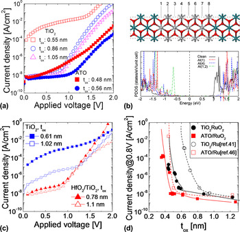
TiO2 is a well-known n-type material due to electron self-doping by oxygen vacancies as mentioned above. It can be expected that acceptor doping into the rutile TiO2 will compensate for oxygen vacancies in the TiO2 and lower the pinned Fermi level, resulting in increased Schottky barrier height. Al ions were used as the acceptor because of the nominal valence state of +3 and the well-established ALD process of Al2O3 thin films. Indeed, aluminum (Al) doping into the rutile TiO2 films remarkably improved the leakage properties of the films. Figure 4(a) shows the leakage current density versus applied voltage (J-V) curves of rutile TiO2 and Al-doped TiO2 (ATO) films grown on Ru by ALD.Reference Kim, Choi, Lee, Seo, Lee, Han, Ahn, Han and Hwang47 Despite the lower t ox of the ATO films, they exhibited better leakage properties over all voltage ranges. At a t ox value as low as 0.5 nm, in particular, the Al-doping significantly reduced the leakage currents of the TiO2 films by ∼106 times at an applied voltage of ∼0.8 V, which is an expected operating voltage of next-generation DRAM capacitors. From the analysis of the conduction mechanism and the valence band offset measurement by XPS, it was verified that the improvement in the leakage properties by Al doping resulted from the increase in the Schottky barrier height by ∼0.5 eV.Reference Kim, Choi, Lee, Seo, Lee, Han, Ahn, Han and Hwang47 First-principle calculations also showed that Al doping into TiO2 lowers the Fermi level without changing the E g of TiO2 [Fig. 4(b)]. Interestingly, the Al ions doped at metal/TiO2 interface regions increase the Schottky barrier height more effectively. Actually, ALD-grown ATO films have higher Al concentration at the vicinity of the interface. This high interfacial Al concentration contributed to a larger effective increase the Schottky barrier height at the ATO/Ru interface.
(a) J–V curves of rutile TiO2 and ATO films on Ru electrodes (data reproduced from Ref. Reference Kim, Choi, Lee, Seo, Lee, Han, Ahn, Han and Hwang47). (b) The side view of the unit cell of the model system for first-principles calculations. TiO2 layer is sandwiched between metallic electrodes of RuO2. Also shown in (b) is the partial density of states (PDOS) projected onto 5th layer of TiO2 for various cases of Al doping. The number in parentheses indicates the layer where the Al atoms are doped. The Fermi level is set to zero in all cases (vertical dashed line). (Figure and data reproduced from Ref. Reference Kim, Choi, Lee, Seo, Lee, Han, Ahn, Han and Hwang47.) (c) J–V curves of TiO2/Ru and thin HfO2/TiO2/Ru stacks (data reproduced from Ref. Reference Seo, Kim, Han and Hwang48). (d) The J level at an applied voltage of 0.8 V versus t ox value of TiO2 and ATO films grown on Ru and RuO2, respectively (data reproduced from Ref. Reference Han, Han, Lee, Lee, Kim, Gatineau, Dussarrat and Hwang44). (Permissions acquired from Wiley-VCH, American Chemical Society, and the American Institute of Physics, respectively.)

Another approach to increase Schottky barrier height is adopting a very thin hafnium oxide (HfO2) layer on the top of rutile TiO2 films.Reference Seo, Kim, Han and Hwang48, Reference Seo, Rha, Kim, Han, Lee, Han and Hwang49 Although an extremely thin HfO2 layer (<1 nm) was deposited on the rutile TiO2 films to minimize the sacrifice in capacitance, the thin HfO2 layer considerably reduced the leakage current of the TiO2 films as shown in Fig. 4(c). An extremely low t ox value of 0.41 nm was reported from a 0.5-nm thick HfO2/TiO2 multilayer, which of course had stable leakage properties.Reference Seo, Kim, Han and Hwang48 The leakage current analysis from quantum mechanical transport simulations revealed that the top HfO2 layer reduced the defect density in the TiO2 film, resulting in increased potential barrier height.Reference Seo, Rha, Kim, Han, Lee, Han and Hwang49 Careful optimization of the physical thickness of the HfO2 layers is required to suppress the loss of capacitance.
Another approach to achieve ultralow leakage currents is to increase the potential barrier height at the metal/TiO2 interface by the use of metals with high work functions. Ru, which serves the growth of rutile TiO2 films at low temperatures, has a work function of ∼4.7 eV. However, this value is lower than the values of the other noble metals such as platinum (Pt), gold (Au), and Ir, which could have better leakage properties. It should be reminded that an important prerequisite in the selection of metal electrode is that the metal has to induce the rutile structure of TiO2 films. RuO2 is a good candidate for this purpose because RuO2 has higher work function (∼5.0 eV) as well as a rutile structure to induce the growth of rutile TiO2 films. Figure 4(d) shows the leakage current density (J) value at an applied voltage of 0.8 V versus t ox value curves of TiO2 and ATO films grown on both Ru and RuO2 electrodes, respectively.Reference Han, Han, Lee, Lee, Kim, Gatineau, Dussarrat and Hwang44 TiO2 and ATO films grown on the RuO2 electrodes clearly showed better dielectric performance compared with the dielectric films grown on the Ru electrodes. In particular, the ATO films on the RuO2 electrodes achieved a t ox of 0.46 nm with stable leakage properties.Reference Han, Han, Lee, Lee, Kim, Gatineau, Dussarrat and Hwang44 It was reported that the improvement in the leakage characteristics is attributed to the increase of potential barrier height that comes from the high work function of the RuO2. An interesting fact is that rutile TiO2 films on the Ru substrate also have an ultrathin RuO2 layer (∼1 nm) at the interface that is in situ formed during the initial growth. The ultrathin RuO2 layer on Ru has lower work function than that of the bulk material due to the carrier redistribution between Ru and RuO2. Therefore, the thick RuO2 with a high work function effectively suppressed the leakage currents of the TiO2 (and ATO) films. From the fact that the lower layer in the bilayered electrode still determines the electrode properties of the very thin top metal layer, it can be inferred that the replacement of the underlayer can improve the leakage properties of a TiO2/metal stack as well. Iridium (Ir) has a much higher work function compared with Ru, with typical values being in the range of ∼5.3 eV. The authors reported that rutile TiO2/thin IrO2/Ir structures shows better dielectric performance compared with the TiO2 films on Ru despite the quite low work function of IrO2(∼4.2 eV).Reference Kim, Han, Han, Lee and Hwang46
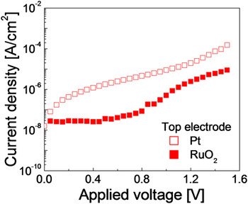
The top electrode also plays a crucial role in improving the capacitance density. Figure 5 shows the J–V curve of a bottom RuO2/8.7-nm thick ATO/top RuO2/TiN sample where the capacitance density of this specific sample corresponds to a t ox of ∼0.40 nm. The J–V curve of another ATO film, this time with a Pt top electrode that showed a similar t ox (of which thickness was 8.0 nm) was also included for comparison. It can be understood that the J level of the former was smaller than that of the latter by ∼2 orders of magnitude at 0.8 V thanks to the larger physical thickness even though the capacitance density was identical. Achieving the same t ox from the thicker ATO film in the former case suggests that the effective value for dielectric constant of the ATO film, although they were identically processed, is higher, which is most probably from the suppression of the intrinsic dead layer effectReference Hwang50–Reference Stengel and Spaldin52 at the top interface due to the adoption of a conducting oxide as the top electrode.
J–V curves of ATO films (t ox: ∼0.4 nm) with RuO2 and Pt top electrodes, respectively.

V. ALD TiO2 THIN FILMS FOR ReRAMs
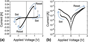
RS materials have bistable low- and high resistance states and which can be arbitrarily controlled by external electrical signals. Here the process that changes the high resistance state to the low resistance state is called a “set” process and the reverse process is called a “reset” process. In the early stages of ReRAM research around the year 2000, the switching mechanism was categorized into unipolar and bipolar RS, where unipolar means the set and reset operations can be performed by the same bias polarity and bipolar means that this can be done by different bias polarity. Figures 6(a) and 6(b) show the current–voltage (I–V) curves measured in electroformed Pt/TiO2/Pt structures for URS and BRS cases, respectively. This classical categorization is purely based on externally observed phenomena and thus does not include any physical implications. During the last decade, the RS mechanism has been intensively studied by many groups and they are now well categorized with greatly expanded knowledge on the underlying science of the phenomena. In this process, TiO2 played a pivotal role due to the following reasons. First, TiO2 is a material that has been thoroughly studied as a high-k capacitor oxide meaning that the deposition and fabrication processes such as CVD, sputtering and ALD and the material properties are well known, allowing researchers to easily approach TiO2 for their ReRAM study. Second, a unique aspect of TiO2 is that it shows both unipolar and bipolar RS, making it easier to study both switching mechanisms and even their correlations.Reference Jeong, Schroeder and Waser53, Reference Kim, Choi, Lee, Kim, Song, Seok, Yoon, Han and Hwang54 One of the major reasons for the confusions and complications among the various RS mechanisms is that one has to deal with a variety of materials that each has its own explanations. The simultaneous presence of both types of RS behavior in a single material clarifies many issues related with the diversity of materials. In this section, therefore, the two RS types (thermochemical type unipolar RS and electronic type bipolar RS) and their relations in TiO2 are reviewed.
Typical (a) unipolar and (b) bipolar RS switching curves measured in electroformed Pt/TiO2/Pt structure. (data reproduced from Ref. Reference Choi, Jeong, Kim, Rohde, Choi, Oh, Kim, Hwang, Szot, Waser, Reichenberg and Tiedke5. Permission acquired from the American Institute of Physics.)

A. Thermochemical unipolar switching in TiO2
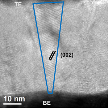
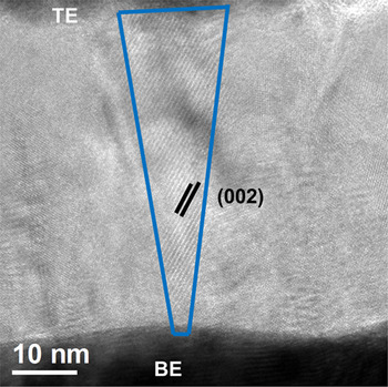
The thermochemical type RS mechanism is closely related to the formation and rupture of local conductive paths called conducting filaments by thermochemical redox reactions in TiO2. The major energy needed in the thermochemical reactions is provided by the Joule heating by the flowing current. Since the Joule heat is barely reliant on bias polarity, unipolar or nonpolar type switching can be explained by means of the thermochemical mechanism.Reference Rohde, Choi, Jeong, Choi, Zhao and Hwang55 In the early stages of research on filamentary switching, conductive atomic force microscopy (CAFM) analysis identified the evolution of conducting filaments at the nanometer scale in URS, although the nature of conducting filaments was far from being clarified.Reference Choi, Jeong, Kim, Rohde, Choi, Oh, Kim, Hwang, Szot, Waser, Reichenberg and Tiedke5, Reference Shin, Lee, Kim, Kim, Song, Seok and Hwang56 However, the recent progress in experimental techniques has demystified the nature of conducting filaments. In fact, it has been experimentally identified that, in TiO2, conducting filaments are made of the Magnéli phases.Reference Kwon, Kim, Jang, Jeon, Lee, Kim, Li, Park, Lee, Han, Kim and Hwang22, Reference Strachan, Pickett, Yang, Aloni, David Kilcoyne, Medeiros-Ribeiro and Williams23 Extensive and careful high-resolution transmission electron microscopy (HRTEM) and electron diffraction analyses showed that the conducting filaments in TiO2 were composed of TinO2n−1 (mostly n = 4 or 5), known as the Magnéli phases (Fig. 7). In situ local I–V measurements in the TEM apparatus clearly indicated that these transformed filaments were indeed highly conductive, implying the filaments could indeed constitute electrical conduction paths. In addition, the resistance of the cell represented a metal-to-insulator transition in a temperature domain when it was cooled down below approximately 130 K. The observed transition temperature corresponds to that of the Magnéli phases, meaning that this further confirmed the Magnéli phase conducting filaments.Reference Kwon, Kim, Jang, Jeon, Lee, Kim, Li, Park, Lee, Han, Kim and Hwang22
High-resolution TEM image of a Ti4O7 nanofilament in Pt/TiO2/Pt structure (data reproduced from Ref. Reference Kwon, Kim, Jang, Jeon, Lee, Kim, Li, Park, Lee, Han, Kim and Hwang22).
For forming the Magnéli phases in the highest titanium oxide, i.e., TiO2, a large number of oxygen-related point defects (mostly oxygen vacancies) should be present in the oxide. However, generally a pristine TiO2 film lacks the number of oxygen vacancies to cause the thermodynamic instability of TiO2. Therefore, an electroforming step is a prerequisite to enable subsequent RS. Electroforming is believed to introduce oxygen vacancies into a TiO2 film, which remarkably increases the local instability of the TiO2 phase, leading to the growth of conducting filaments consisting of lower titanium oxides, i.e., the Magnéli phases. The electroformed state is generally achieved by applying a (soft) breakdown voltage to the TiO2 film with an appropriate compliance current. It is most likely that a large number of nuclei for the conducting filament are formed initially but once an adequate number of them are consumed in connecting both the electrodes, rest of the nuclei stop growing.
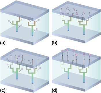
In TiO2, conducting filament formation may be described by a nucleation and growth process. The direction of conducting filament growth was found to be parallel to the direction of electric field, rather than in random direction. Positively charged oxygen vacancies are most likely generated at the anodic interface in a TiO2-based RS cell, as a result of the oxidation of oxygen ions. They could drift and diffuse to the cathode interface by the applied bias and concentration gradient, respectively. During this process, electrons are injected locally at the cathodic interface at a location where the interfacial Schottky barrier is lowered in the Pt/TiO2/Pt system. Figure 8 illustrates the filament nucleation and growth process in detail. Owing to the preferential nucleation at the cathodic interface, the final conducting filament shape could have a conical shape, where wider and narrower diameters are formed at the cathodic and anodic interfaces, respectively.Reference Kwon, Kim, Jang, Jeon, Lee, Kim, Li, Park, Lee, Han, Kim and Hwang22, Reference Kim and Hwang57 This anisotropic shape of the conducting filament is the cause of the several characteristic phenomena of thermochemical RS, including the anodic interface localized switching.Reference Kim, Choi, Shin, Choi and Hwang58, Reference Kim, Choi and Hwang59 Readers are suggested to refer to a recent review article by the authors regarding this issue.Reference Kim, Jeong and Hwang60
The schematic illustration of unipolar RS of TiO2(a) by increasing the applied bias, the conducting filament begins growing from the cathode (electron injection electrode). (b) Once one of filament touches the anode, the MIM system switches to the on state, which is called “forming.” (c) By the reset process, the filament rupturing occurred at the anode interface by reoxidation of conducting filament. (d) By the subsequent set process, the conducting filament is rejuvenated.

The formed filaments are ruptured by the reset process and the ruptured filament can be rejuvenated by the set process. The reset operation might be achieved by melting the Magnéli conducting filaments with sufficient electric current and subsequent cooling down. During the cooling step, the melted material may crystallize into either anatase or rutile depending on the phase of the neighboring TiO2−x material. It is also possible that extremely rapid cooling down occurs, inducing the solidification of the melted material into an amorphous phase. Although the most thermodynamically stable phase in the Ti–O system when such large amounts of oxygen vacancies are present (Ti4O7 is equivalent to TiO1.75) is the Magnéli phase, the possible rapid cooling of the melted material may not allow enough time to form Magnéli phase. This can be understood from the fact that the formation of a Magnéli phase requires the rearrangement of oxygen vacancies on the (121) plane of the rutile TiO2 structure, which may take a significant duration of time. It is clear that these defective anatase or rutile phases (TiO2−δ where δ < 0.25) have much higher electrical conductivity than the pristine stoichiometric TiO2, but it is also possible that this material is much more insulating than the Magnéli phase because a percolating path may not be formed in the TiO2−δ. Indeed, the resistance of the reset state RS sample is generally much lower than that of the pristine sample but is still far higher than the set state.Reference Choi, Jeong, Kim, Rohde, Choi, Oh, Kim, Hwang, Szot, Waser, Reichenberg and Tiedke5 The promising aspect of this model is that it does not require any involvement of the unidirectional motion of oxygen ions during repeated set/reset switching. The material just changes its phase from the metallic (or highly conductive semiconducting) Magnéli to the less conducting defective TiO2−δ. During the subsequent set operations, the flow of current induces a Joule heating effect, which transforms the metastable defective TiO2−δ into the stable Magnéli phase.
B. Electronic or ionic bipolar switching in TiO2
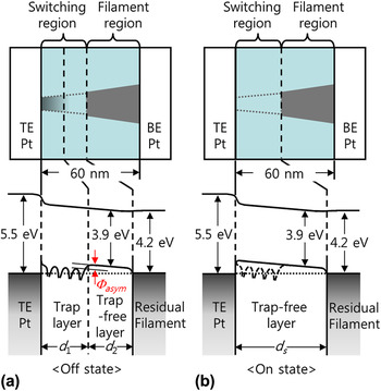
Electronic type BRS corresponds to a case where the trap-mediated hysteretic electronic conduction is asymmetric with respect to the bias polarity.Reference Kim, Choi, Lee, Kim, Song, Seok, Yoon, Han and Hwang54 This can be achieved after the rupture of a conducting filament by the thermochemical reset process. After the filament rupture, the TiO2 can be divided into the filament ruptured region and the filament region. The filament region, which is composed of the Magnéli phase, can be regarded as an electrode forming an Ohmic contact. [The bottom panels of Figs. 9(a) and 9(b)] The filament ruptured region (which is the switching region here) can be divided into two layers, one being the switching layer (TiO2−y) where the RS occurs and the other being the nonswitching layer (TiO2−x) which is inevitable for RS even though no switching occurs. [at x < y, the bottom panels of Figs. 9(a) and 9(b)] The switching layer contains a much higher density of electron traps (probably oxygen vacancies), and the resistance change is caused by the trapping and detrapping of electrons. In this structure, an asymmetric potential barrier of traps (Φ asym) with respect to bias direction, as shown in Fig. 9(a), is presented. When a negative bias is applied, the injected electrons from the top electrode are easily trapped due to the presence of Φ asym. At the trap filling limit voltage, all the traps are filled with electrons and a sudden current jump, which corresponds to set switching, is observed. When a positive bias was applied and reached a reset voltage, the trapped electrons start to escape to the top electrode, resulting in a high resistance state. This is because Φ asym does not act against the detrapping process under a positive bias.
The upper panels show the schematic diagram of (a) high resistance state and (b) low resistance state in top electrode Pt/TiO2−y/TiO2−x/ residual filament structure. The solid conical shape of (a) and (b) represents the residual filaments. The gradient of shading at the TE Pt side of (a) represents the supposed trap distribution; the higher the trap density is, the darker the region. A conical filament is supposed with a gray color. The lower panels show the corresponding band diagrams of the switching region. (Figures reproduced from Ref. Reference Kim, Choi, Lee, Kim, Song, Seok, Yoon, Han and Hwang54.)

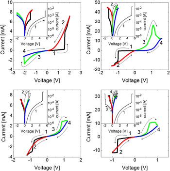
In this electronic switching scheme, the position of the switching layer and the density of traps can be arbitrarily controlled electrically by tuning the filament shape and following filament rupture process.Reference Kim, Kim, Song, Seok, Lee, Yoon and Hwang61 As a result, various bipolar switching configurations can be achieved within the Pt/TiO2/Pt structure as shown in Fig. 10. This result provides a new method of deriving the switching polarity of memristors electrically, which suggests a new path for the application of ReRAM.
Various bipolar switching configurations depending on the various electroforming process achieved within the Pt/TiO2/Pt structure. (data reproduced from Ref. Reference Kim, Kim, Song, Seok, Lee, Yoon and Hwang61.)

Interestingly, the bipolar switching mediated by the ionic migration of oxygen vacancies as well as the trap-mediated electronic bipolar resistive switching occurs in an almost identically prepared unipolar reset TiO2 sample. Although what determines the switching mode is yet to be clarified, apparently it is highly correlated with the oxygen vacancy concentration at the switching region since each switching mechanism works in totally distinguishable conditions. Basically, an electronic bipolar resistive switching happens in the condition where fluent carrier injection into the conduction band of the insulator is guaranteed, whereas an ionic bipolar resistive switching occurs when a substantial Schottky potential barrier is present at the electrode/insulator interface. Therefore, electronic/ionic bipolar resistive switching occurs with low (<∼0.1 eV)/high (>0.2 eV) Schottky barrier height due to the high/low oxygen vacancy concentration near the electrode (>∼1019 to 1020 cm−3). The corresponding ionic bipolar switching was reported as follows.
While an electroformed Pt/TiO2/Pt cell goes through unipolar reset, a bountiful amount of oxygen vacancies are generated at the Magnéli (Ti4O7) filament ruptured region due to the partial reoxidation of Ti4O7 toward TiO2. Affected by the unipolar reset bias, these oxygen vacancies are most likely to reside at the vicinity of the tip of the filament, resulting in an effective microscopic structure of Pt(Top electrode)/TiO2/TiO2−x/Ti4O7(Bottom electrode). The remaining Magnéli filament is considered as the bottom electrode because it shows metallic conduction with a stable vacancy-ordered phase, and should be therefore intact during the subsequent bipolar resistive switching. In the proposed effective microstructure, a bipolar set and reset occurs at negative and positive bias, respectively, near the filament ruptured region. Moreover, owing to the finite amount of oxygen vacancies comprising the TiO2−x layer, a strong negative bias can invert the oxygen vacancy configuration, and in turn, bipolar resistive switching with the other operation polarity is achieved with the effective microstructure of Pt/TiO2−x/TiO2/Ti4O7. This was further supported by a comparison study with a Pt/TiO2/TiO2−x/Pt cell, whose TiO2−x layer was intended to have a much larger oxygen vacancy concentration by inserting a thick Ti layer between the TiO2 and Pt in the device fabrication process, and therefore making the inversion of vacancy configuration through electrical means virtually impossible. In both devices, the high resistance state was fitted clearly to Schottky conduction, which had not been the case in the previously introduced electronic bipolar resistive switching case. The low resistance state, on the other hand, could be described by local conduction through filaments consisting of oxygen vacancies, and this was demonstrated by the fact that no electrode area dependency was found to exist for the resistance in the low resistance state.Reference Yoon, Lee, Kim, Song, Seok, Han, Yoon, Kim and Hwang62
It is noteworthy that the bipolar resistive switching is caused by the localized drift of oxygen vacancies, unlike other material systems where the homogeneous migration of oxygen vacancies over interfacial area is commonly known as the main cause of this type of switching.Reference Sawa3 In addition, Yang et al. elucidated the mechanism for bipolar resistive switching in a single crystalline TiO2 in the same way, implying that the localized drift of oxygen vacancies along the direction of electric field is highly probable to occur, particularly in this type of material system, i.e., TiO2, even without favorable defect migration sites such as grain boundaries.Reference Yang, Pickett, Li, Ohlberg, Stewart and Williams63 The results discussed above clearly reveal the diversity of the resistance switching phenomena in TiO2. Although this may induce some confusion and dispute for the accurate understanding of the RS mechanism in several other oxide systems, TiO2 actually provides a representative material system that can test the diverse behaviors of any RS material.
VI. CONCLUSION AND OUTLOOK
In this review article, the intriguing and promising electrical properties of TiO2 thin films as a high-k dielectric layer for DRAM capacitors, requiring extremely high level of insulating property with minimal density of defects, and as a resistance switching layer for ReRAM, relying upon the generation of high density of defects and their percolation, are discussed. While the DRAM application requires rutile-structured TiO2 films, of which the value for dielectric constant is the highest among the known binary oxides, TiO2 films for ReRAM actually does not show a critical dependence on their phase. The rutile TiO2 film can be obtained with the help of local epitaxy with the substrate electrode, such as RuO2 or IrO2, even at the temperature range where the ALD process is possible (<∼300 °C) which is inevitable for the high integration density of DRAM as well as ReRAM. The already high insulating properties of the TiO2 material are even further strengthened by doping the material with Al2O3, which slightly sacrifices the very high-k value of the rutile TiO2 while maintaining its rutile structure. ReRAM application of TiO2, on the other hand, requires an electroforming step, which actually forms a lot of defects in the material in a controlled manner.
Fabricating mass-production compatible memory device heavily depends on the materials functionality and performance. An easy and economical fabrication process is as important as the material’s functionality with that regard. The ALD processes of TiO2 are highly developed, and no obvious difficulties are expected at this moment. Therefore, it is very possible that TiO2 or TiO2-based materials will be adopted in the above-mentioned devices. However, several issues still remain to be cleared out for these applications before these devices are available in everyday life. The reliability of the dielectric and resistance switching performances of the TiO2 films is one of the most critical issues yet to be cleared. Despite such difficulties, there are a great deal of research efforts and developments going on all over the world, which will facilitate solving these issues and problems and make TiO2 an essential material in solid state memory devices of the future.
ACKNOWLEDGMENTS
This work was supported by the IT R&D program of MKE/KEIT [KI002178, Development of a mass production compatible capacitor for next-generation DRAM], the Converging Research Center Program through the National Research Foundation of Korea (2011K000610), the National Research Program for the Nano Semiconductor Apparatus Development sponsored by the Korea Ministry of Knowledge and Economy (10034831), and World Class University program through the Korea Science and Engineering Foundation funded by the Ministry of Education, Science and Technology (R31-2008-000-10075-0).