Introduction
New multifunctional materials and systems are highly sought after in modern electronics. Strongly correlated oxides are ideal materials for realizing such multifunctional properties because they exhibit a wide range of properties arising from the strong interplay among the structural, electronic, magnetic, and even ionic degrees of freedom. Reference Imada, Fujimori and Tokura1,Reference Dagotto2 One highly topical example that has been widely explored is electrically switchable magnetic memory for realizing the sought-after goal of low-power, nonvolatile random-access memory. Reference Ramesh and Spaldin3–Reference Cheong and Mostovoy5 In the absence of single-phase materials exhibiting sizable magnetoelectric coupling effects at room temperature, coupled oxide systems have been widely studied, as discussed in the article in this issue by Hu et al. Heterointerfaces of oxide materials are also important for realizing new physical phenomena. Reference Yamada, Ogawa, Ishii, Sato, Kawasaki, Akoh and Tokura6–Reference Hwang, Iwasa, Kawasaki, Keimer, Nagaosa and Tokura8 The most widely known example of this is exhibited by the polar interfaces in LaAlO3/SrTiO3 (LAO/STO) heterostructures. A highly conducting two-dimensional electron gas is formed at the interface between the two insulators, Reference Ohtomo and Hwang9 which shows great potential for a new class of high-frequency transistors. Many other artificial oxide superlattices have also been studied, and completely unexpected phenomena, including magnetic, Reference Brinkman, Huijben, van Zalk, Huijben, Zeitler, Maan, van der Wiel, Rijnders, Blank and Hilgenkamp10 ferroelectric, Reference Lee, Christen, Chisholm, Rouleau and Lowndes11 and ionic Reference Garcia-Barriocanal, Rivera-Calzada, Varela, Sefrioui, Iborra, Leon, Pennycook and Santamaria12 effects, have been reported.
In parallel with the large range of novel functionalities enabled by high-quality planar heterointerfaces, heteroepitaxial nanocomposite thin films composed of at least one strongly correlated metal oxide coupled with another synergistically selected oxide have emerged as a new thin-film device platform in the past decade. Reference Zheng, Wang, Lofland, Ma, Mohaddes-Ardabili, Zhao, Salamanca-Riba, Shinde, Ogale, Bai, Viehland, Jia, Schlom, Wuttig, Roytburd and Ramesh13–Reference Liu, Liang, Chu, Zheng and Ramesh17 Such structures offer a promising alternative to conventional planar films for future nanoelectronics needs. In this article, we review recent advances in nanocomposite architectures formed by two epitaxial phases in a film-on-substrate geometry, with a focus on vertically aligned nanocomposites (VANs). First, we introduce different growth mechanisms in various self-assembled nanocomposite films and discuss important factors affecting their morphologies and pillar dimensions. Second, we highlight several key functionalities tailored by the strong coupling between the two phases and the interface effects, including enhanced flux pinning in high-temperature superconductors, Reference MacManus-Driscoll, Foltyn, Jia, Wang, Serquis, Civale, Maiorov, Hawley, Maley and Peterson18–Reference Llordés, Palau, Gázquez, Coll, Vlad, Pomar, Arbiol, Guzmán, Ye, Rouco, Sandiumenge, Ricart, Puig, Varela, Chateigner, Vanacken, Gutiérrez, Moshchalkov, Deutscher, Magen and Obradors20 strain-enhanced ferroelectricity and multiferroics, Reference Zheng, Wang, Lofland, Ma, Mohaddes-Ardabili, Zhao, Salamanca-Riba, Shinde, Ogale, Bai, Viehland, Jia, Schlom, Wuttig, Roytburd and Ramesh13,Reference Harrington, Zhai, Denev, Gopalan, Wang, Bi, Redfern, Baek, Bark, Eom, Jia, Vickers and MacManus-Driscoll21–Reference Choi, Weal, Bi, Wang, Kursumovic, Fix, Blamire and MacManus-Driscoll24 enhanced ferromagnetism, Reference Wang, Li, Viswan, Hu, Harris, Li and Viehland25–Reference Weal, Patnaik, Bi, Wang, Fix, Kursumovic and MacManus Driscoll27 magnetoresistance, Reference Chen, Bi, Tsai, Lee, Su, Zhang, Jia, MacManus-Driscoll and Wang28,Reference Zhang, Chen, Khatkhatay, Tsai, Su, Jiao, Zhang and Wang29 novel electronic/ionic transport, Reference Hsieh, Liou, Huang, Liang, He, Zhan, Chiu, Chen and Chu30–Reference Lee, Sangle, Lu, Chen, Zhang, Lee, Wang, Jia and MacManus-Driscoll32 and novel coupled dielectric and optical effects. Reference MacManus-Driscoll, Zerrer, Wang, Yang, Yoon, Fouchet, Yu, Blamire and Jia33–Reference Liu, Chen, He, Liang, Chen, Chien, Hsieh, Lin, Arenholz, Luo, Chueh, Chen and Chu35 Finally, we discuss the challenges in designing different nanocomposite structures and related physical properties before proposing future directions.
Heteroepitaxial nanocomposite systems and their growth control
Self-assembled vertically aligned nanocomposites (VANs) form as a consequence of a few key attributes: (1) a close lattice match between two phases and/or a crystal-symmetry-based interrelationship between them (e.g., perovskites and spinels); (2) an epitaxial relationship of the main matrix phase with the substrate, thus seeding the initial growth of the film; (3) low solubility of the two phases in one another; and (4) preferably similar crystal chemistries between the two phases. Thus, a good starting point for materials selection is to examine the bulk phase diagram of ternary or quaternary systems based on the two phases selected.
A thin-film kinetic growth process should be considered because lattice strain and surface energy play significant roles in controlling the overall film morphology. Although it is challenging to predict the extent to which bulk thermodynamics can be overcome by epitaxial constraint, it is prudent to consider both criteria to achieve nanocomposite films with vertical heteroepitaxy. Specific parameters are thus involved in the material design, including matching of crystal structures, lattice parameters, and different cation radii/charges in the two phases. If the appropriate phase diagram does not exist, a good strategy is to choose phases whose cation radii and charges are quite different. This was the approach taken to create the first nanocomposite films of YBa2Cu3O7−x (YBCO) + BaZrO3: Considering BaZrO3, Ba2+ exists in both phases as desired, but Zr4+ is a smaller and more highly charged ion, so intermixing with Cu2+/3+ and Ba2+ ions in YBCO is not expected. Some intermixing with Y3+, on the other hand, is expected.
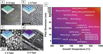
Figure 1 shows schematics of the most common nanocomposite architectures: nanoparticle-embedded nanocomposites [YBa2Cu3O7−δ-BaZrO3 (YBCO-BZO), Figure 1a], Reference Llordés, Palau, Gázquez, Coll, Vlad, Pomar, Arbiol, Guzmán, Ye, Rouco, Sandiumenge, Ricart, Puig, Varela, Chateigner, Vanacken, Gutiérrez, Moshchalkov, Deutscher, Magen and Obradors20 vertically aligned nanocomposites [VANs; BaTiO3-Sm2O3 (BTO-SmO), Reference Harrington, Zhai, Denev, Gopalan, Wang, Bi, Redfern, Baek, Bark, Eom, Jia, Vickers and MacManus-Driscoll21 Figure 1b; BiFeO3-CoFe2O4 (BFO-CFO) Reference Zheng, Straub, Zhan, Yang, Hsieh, Zavaliche, Chu, Dahmen and Ramesh36 , Figure 1c], and laminated nanocomposites (YBCO-BZO, Figure 1d). Reference Zhao, Li, Lee, Choi, Liang, Zhang, Tang, Wang, Jia, MacManus-Driscoll and Yang37 It is noteworthy that such nanocomposites are self-assembled mostly by physical vapor deposition and chemical solution-based deposition, without control of the deposition sequence, as is required for multilayer/superlattice films. In particular, easy dimensional tunability has been demonstrated in 1–3-type VAN films, in which various nanopillar shapes and dimensions (2–200 nm) have been achieved in specific material systems. Reference Zheng, Wang, Lofland, Ma, Mohaddes-Ardabili, Zhao, Salamanca-Riba, Shinde, Ogale, Bai, Viehland, Jia, Schlom, Wuttig, Roytburd and Ramesh13,Reference Zhang, Chen, Bi, Jia, MacManus-Driscoll and Wang16,Reference Harrington, Zhai, Denev, Gopalan, Wang, Bi, Redfern, Baek, Bark, Eom, Jia, Vickers and MacManus-Driscoll21,Reference Fix, Choi, Robinson, Lee, Chen, Prasad, Wang, Blamire and MacManus-Driscoll23,Reference Zhang, Jian, Chen, Jiao, Khatkhatay, Li, Chu, Jia, MacManus-Driscoll and Wang26,Reference Lee, Sangle, Lu, Chen, Zhang, Lee, Wang, Jia and MacManus-Driscoll32–Reference Bonilla, Novikova, Vidal, Zheng, Fonda, Demaille, Schuler, Coati, Vlad, Garreau, Sauvage Simkin, Dumont, Hidki and Etgens46 To design versatile VAN architectures with desired functionalities, a fundamental understanding of the different growth mechanisms is needed. In the following section, we discuss the formation mechanism of VAN systems grown by pulsed laser deposition. The equilibrium microstructure of a two-phase nanocomposite film is largely determined by the thermodynamic stability of the two component phases. Depending on the chemical miscibility, the starting mixture in the target will form VAN films by either (1) nucleation and growth or (2) (pseudo-) spinodal decomposition growth. Reference MacManus-Driscoll14
(a) A 0–3-type nanocomposite of BaZrO3 (BZO) nanoparticles in a YBa2Cu3O7−x (YBCO) matrix; a 1–3-type vertically aligned nanocomposite (VAN) of (b) Sm2O3 nanopillars in a BaTiO3 matrix; (c) CoFe2O4 nanopillars in a BiFeO3 matrix; and (d) a 2–2-type laminated structure formed in heteroepitaxial nanocomposite films of YBCO (Y) and BZO (B). The notation indicates whether connectivity of the nanomaterial (first number) and matrix (second number) is in zero, one, two, or three dimensions. (e) Pillar dimension as a function of growth temperature in 1–3-type VAN structures with various morphologies. The different symbols represent actual nanopillar shapes (columnar, square, triangular, and hexagonal). Numbers in parentheses represent the molar fraction of the secondary phase; (111) represents the out-of-plane growth orientation. (a) Reproduced with permission from Reference 20. © 2012 Nature Publishing Group. (b) Reproduced with permission from Reference 21. © 2011 Nature Publishing Group. (c) Reproduced with permission from Reference 36. © 2006 Wiley-VCH. (d) Reproduced with permission from Reference 37. © 2014 Wiley-VCH.

The growth of most nanocomposite systems is dominated by the mechanism of nucleation and growth. Reference Zheng, Straub, Zhan, Yang, Hsieh, Zavaliche, Chu, Dahmen and Ramesh36 In brief, in VAN films with two immiscible phases, the phase with a higher interfacial energy γ1 (lower wettability) with the substrate forms nuclei that grow into pillars, whereas the other phase, with a lower interfacial energy γ2, undergoes layer-by-layer growth and becomes the planar matrix. Spinodal or pseudospinodal decomposition growth occurs in certain systems, Reference MacManus-Driscoll14,Reference Kang, Wang, MacManus-Driscoll, Li, Jia, Mihut and Betts47–Reference Ni, Rao and Khachaturyan50 giving rise to spatially ordered structures. In both mechanisms, product phases gradually develop from a parent solid solution phase in which cations can intermix, but pseudospinodal decomposition involves a symmetry-lifting crystal lattice rearrangement. More detailed discussion for the nanocomposite film growth mechanism can be found in previous topical reports. Reference MacManus-Driscoll14,Reference Zheng, Straub, Zhan, Yang, Hsieh, Zavaliche, Chu, Dahmen and Ramesh36,Reference Park, Horibe, Asada, Wielunski, Lee, Bonanno, O’Malley, Sirenko, Kazimirov, Tanimura, Gustafsson and Cheong49,Reference Ni, Rao and Khachaturyan50 Figure 1e summarizes recent heteroepitaxial two-phase nanocomposite systems with self-assembled vertical nanopillars embedded in a planar matrix. Reference Zheng, Wang, Lofland, Ma, Mohaddes-Ardabili, Zhao, Salamanca-Riba, Shinde, Ogale, Bai, Viehland, Jia, Schlom, Wuttig, Roytburd and Ramesh13,Reference Zhang, Chen, Bi, Jia, MacManus-Driscoll and Wang16,Reference Harrington, Zhai, Denev, Gopalan, Wang, Bi, Redfern, Baek, Bark, Eom, Jia, Vickers and MacManus-Driscoll21,Reference Fix, Choi, Robinson, Lee, Chen, Prasad, Wang, Blamire and MacManus-Driscoll23,Reference Zhang, Jian, Chen, Jiao, Khatkhatay, Li, Chu, Jia, MacManus-Driscoll and Wang26,Reference Lee, Sangle, Lu, Chen, Zhang, Lee, Wang, Jia and MacManus-Driscoll32–Reference Bonilla, Novikova, Vidal, Zheng, Fonda, Demaille, Schuler, Coati, Vlad, Garreau, Sauvage Simkin, Dumont, Hidki and Etgens46 The pillar dimensions and actual shapes (represented by square, stripe, triangular, circular and hexagonal symbols) are plotted as a function of growth temperature. More work is needed both to further understand the fundamental growth mechanisms of (pseudo-) spinodal thin-film systems, and to predict and experimentally verify new highly ordered nanostructured composites.
Wide-ranging VAN compositions and functionalities
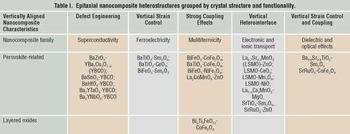
Unique VAN architectures have several key advantages over conventional planar heterostructures, including simpler self-assembled growth, a higher density of vertical heterointerfaces and associated defects in some cases, efficient strain control, and strong coupling effects. By utilizing such characteristics in specific VAN heterostructures, a wide range of nanoscale functionalities have been achieved, as summarized in Table I . Next, examples of several individual functionalities are discussed in more detail.
Epitaxial nanocomposite heterostructures grouped by crystal structure and functionality.

Flux pinning in high-temperature superconductors
We begin our exploration of nanocomposite functionalities by summarizing the status of the YBCO system. Even though the YBCO-BZO system is used in large-area coated conductor films for power applications rather than in small-scale electronic devices, the subject of this article, exactly the same underlying principles apply for other nanocomposite composition systems as for YBCO. Furthermore, because the YBCO-BZO system is already used in industry, the rapid success of YBCO paved the way for the emergence of a range of other electronic devices using nanocomposite films. Reference Larbalestier, Gurevich, Feldmann and Polyanskii51–Reference MacManus-Driscoll, Harrington, Durrell, Ercolano, Wang, Lee, Tsai, Maiorov, Kursumovic and Wimbush53
For oxide superconductor-based high-efficiency power transmission and superconducting generators and motors, high critical current densities (J c) are required under an applied magnetic field in long-length coated conductors made by physical or chemical thin-film routes. The ability of a Type II superconductor to carry supercurrent under an applied magnetic field is referred to as flux pinning. J c is very sensitive to structural defects such as dislocations, grain boundaries, second phases, cracks, and voids, because such defects provide effective pinning centers for flux vortices and thus sustain high J c. Reference Foltyn, Civale, MacManus-Driscoll, Jia, Maiorov, Wang and Maley52 In the past decade, the flux-pinning properties of high-temperature superconductors have been markedly improved, and an understanding about how nanocomposites grow and how they can be tuned to enhance flux pinning has emerged. Reference MacManus-Driscoll, Harrington, Durrell, Ercolano, Wang, Lee, Tsai, Maiorov, Kursumovic and Wimbush53–Reference Xu, Delgado, Khatri, Liu, Selvamanickam, Abraimov, Jaroszynski, Kametani and Larbalestier65
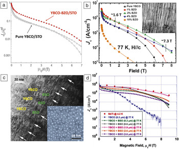
Incorporating BaZrO3 (BZO) nanoparticles in epitaxial YBa2Cu3O7 (YBCO) films was demonstrated as the first successful approach to generating high-density defect pinning centers, and strong improvement of J c ( Figure 2a) was achieved. Reference MacManus-Driscoll, Foltyn, Jia, Wang, Serquis, Civale, Maiorov, Hawley, Maley and Peterson18 In the past few years, significant further progress has been made to achieve highly tuned (in terms of size, density, and length) columnar defects, formed from a variety of compounds containing group 4 and 5 elements. Reference MacManus-Driscoll, Harrington, Durrell, Ercolano, Wang, Lee, Tsai, Maiorov, Kursumovic and Wimbush53 Figure 2b shows such an example in which columnar defects introduced by self-assembled BZO nanopillars in the YBCO matrix were fabricated. Reference Wee, Zuev, Cantoni and Goyal55 The defect density can be systematically tailored by controlling the BZO nanocolumn density and spacing so that the optimal J c value is achieved over a wide field and angular range. Highly ordered VAN structures have also been achieved in YBCO-BaSnO3 (BSO) nanocomposite films (Figure 2c), and enhanced J c values have been maintained at high magnetic fields by increasing the film thickness (Figure 2d). Reference Varanasi, Burke, Wang, Lee and Barnes56 This nanocomposite approach to enhancing the YBCO flux-pinning properties has already been successfully achieved by incorporating a wide range of materials systems, including BaZrO3, Reference MacManus-Driscoll, Foltyn, Jia, Wang, Serquis, Civale, Maiorov, Hawley, Maley and Peterson18,Reference Wee, Zuev, Cantoni and Goyal55 BaSnO3, Reference Zhu, Tsai, Wang, Kwon, Wang, Varanasi, Burke, Brunke and Barnes43,Reference Varanasi, Burke, Wang, Lee and Barnes56 BaHfO3, Reference Sieger, Hänisch, Iida, Gaitzsch, Rodig, Schultz, Holzapfel and Hühne57 BaMnO3, Reference Paolo, Kaname, Tomoya, Ataru, Masashi, Yutaka, Shigeru and Ryusuke58 REBa(Ta/Nb)O6 (RE = Er, Gd, and Yb), Reference Harrington, Durrell, Maiorov, Wang, Wimbush, Kursumovic, Lee and MacManus-Driscoll59,Reference Ercolano, Harrington, Wang, Tsai and MacManus-Driscoll60 Fe2O3-CeO2, Reference Tsai, Huang, Lee, Khatkhatay, Chen, Chen, Su and Wang61 and CoFe2O4-CeO2, Reference Huang, Tsai, Chen, Jian, Khatkhatay, Yu and Wang62,Reference Chen-Fong, Li, Aiping, Khatkhatay, Wenrui and Haiyan63 as well as other complex oxides. Reference Ercolano, Bianchetti, Wimbush, Harrington, Wang, Lee and MacManus-Driscoll64,Reference Xu, Delgado, Khatri, Liu, Selvamanickam, Abraimov, Jaroszynski, Kametani and Larbalestier65
(a) Critical current density J c/J c sf of pure YBa2Cu3O7−x (YBCO) and YBCO- BaZrO3 (BZO) nanocomposite films on SrTiO3 (STO) as a function of the applied magnetic field μ0 H, where J c and J c sf represent the critical current density with and without an applied magnetic field (sf, self-field), respectively. (b) Magnetic-field-dependent J c values of YBCO-BZO nanocomposite films with different compositions, measured at 77 K and with an out-of-plane magnetic field. Inset: Cross-sectional transmission electron microscopy (TEM) image of 4 vol% BZO nanopillars in YBCO. (c) Cross-sectional TEM image of a 3.6-μm-thick YBCO-BaSnO3 (BSO) nanocomposite film. Inset: Corresponding top-view scanning electron microscopy image. (d) J c values of YBCO-BSO nanocomposite films with different thicknesses compared with that of a 300-nm-thick pure YBCO film and NbTi as a standard reference. (a) Reproduced with permission from Reference 18. © 2004 Nature Publishing Group. (b) Reproduced with permission from Reference 55. © 2013 Nature Publishing Group. (c–d) Reproduced with permission from Reference 56. © 2008 American Institute of Physics.

Vertical strain-enhanced ferroelectricity
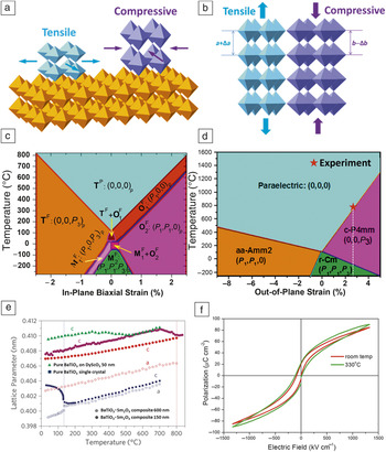
Strain engineering of ferroelectric thin films has been established as an effective way to control the tetragonal-to-cubic structural transition in ferroelectrics ( Figure 3a–c). Reference Haeni, Irvin, Chang, Uecker, Reiche, Li, Choudhury, Tian, Hawley, Craigo, Tagantsev, Pan, Streiffer, Chen, Kirchoefer, Levy and Schlom66–Reference Li and Chen69 However, the substrate-induced biaxial strain can only be maintained in ultrathin films up to a few tens of nanometers in thickness (i.e., in the so-called pseudomorphic growth regime). Reference MacManus-Driscoll, Zerrer, Wang, Yang, Yoon, Fouchet, Yu, Blamire and Jia33 Beyond that, structural defects such as dislocations and boundaries usually appear, relaxing the strain and degrading the physical properties.
Schematics of (a) substrate-induced biaxial strain and (b) vertical lattice strain in vertically aligned nanocomposites (VANs), where a + Δa and b – Δb represent strain-induced lattice parameters. Temperature-dependent (c) in-plane and (d) out-of-plane strain phase diagrams of BaTiO3 (BTO) films. TP, TF, OF, and MF represent tetragonal paraelectric, tetragonal ferroelectric, orthorhombic ferroelectric, and monoclinic ferroelectric phases, respectively, and P i represents the corresponding polarization vector. The notations of aa, c, and r represent orthorhombic, tetragonal and monoclinic phase, respectively. (e) Temperature dependence of lattice parameters of pure BTO film and BTO-Sm2O3 (SmO) VAN films (filled symbols, out-of-plane lattice parameter c; hollow symbols, in-plane parameter a). (f) Ferroelectric polarization-voltage hysteresis loop of 1-μm BTO-SmO thin-film capacitors at room temperature and 330°C. (a–b) Reproduced with permission from Reference 16. © 2014 Elsevier. (c) Reproduced with permission from Reference 69. © 2006 American Institute of Physics. (d) Reproduced with permission from Reference 70. © 2013 Springer. (e–f) Reproduced with permission from Reference 21. © 2011 Nature Publishing Group.

On the other hand, high-strain states can be maintained in thick VAN films for practical device applications by vertical lattice strain coupling of two epitaxial phases with different elastic moduli and lattice parameters (Figure 3b). Reference Liu, Liang, Chu, Zheng and Ramesh17 Figure 3d shows the out-of-plane strain phase diagram of (001)-oriented BTO in thick VAN nanostructures with full relaxation of the in-plane strain. This theoretical work was inspired by, and explains, the previous experimental study of thick BTO-SmO VAN films grown on STO. Reference Wu, Chai, Xu, Li and Zhang70 Specifically, stiff SmO nanocolumns, grown in a self-assembled manner within a BTO matrix of micrometer-thick films, produced a large out-of-plane tensile strain of ∼2–3% in the BTO, which led to the maintenance of tetragonality and ferrroelectric polarization to at least 800°C—much higher than the conventional phase transition temperature (130°C) of BTO single crystals (Figure 3e). Reference Harrington, Zhai, Denev, Gopalan, Wang, Bi, Redfern, Baek, Bark, Eom, Jia, Vickers and MacManus-Driscoll21 Robust ferroelectric polarization in BTO-SmO VAN films was measured at 330°C without any degradation, compared to its room-temperature behavior (Figure 3f). BTO-SmO nanocomposite films were further fabricated into nontoxic microactuators that performed even better than Pb[Zr x ,Ti1–x ]O3-based structures at high temperatures. Reference Kursumovic, Defay, Lee, Tsai, Bi, Wang and MacManus-Driscoll71
Other studies of ferroelectric VAN films were undertaken with the BFO-SmO system. Unlike the BTO-SmO system, which involves very little Sm3+ substitution for Ba2+, so that nucleation and growth is the predominant mechanism of film formation, in BFO-SmO, a considerable substitution of Sm3+ in the Bi3+ site occurs, which allows for spinodal decomposition. Reference Karimi, Reaney, Han, Pokorny and Sterianou72 Sm-doped BFO-SmO nanocomposite films showed the combined advantages of enhanced polarization from Sm doping and a lower dielectric loss because of the out-of-plane compressive strain in BFO. Reference Yang, Wang, Yoon, Wang, Jain, Feldmann, Dowden, MacManus-Driscoll and Jia73 The films form an ordered checkerboard structure that could also be readily strain-tuned by tuning the growth rate and, hence, the column size; consequently, the losses were considerably lowered. Reference Bi, Lee, Yang, Jia, MacManus-Driscoll and Wang74
Strain-coupled magnetoelectrics
Robust magnetoelectric coupling in a simple, self-assembled epitaxial nanocomposite system was first demonstrated in the BTO-CFO system, where ferrimagnetic CFO nanopillars were embedded in a ferroelectric BTO matrix. Reference Zheng, Wang, Lofland, Ma, Mohaddes-Ardabili, Zhao, Salamanca-Riba, Shinde, Ogale, Bai, Viehland, Jia, Schlom, Wuttig, Roytburd and Ramesh13 The elastic interaction of BTO and CFO at vertical epitaxial interfaces facilitates a strong coupling between the electrical polarization and magnetic order. After this pioneering work, carried out around the same time as the first nanocomposites in YBCO systems were demonstrated, tremendous research efforts, both experimental and theoretical, have focused on investigating epitaxial nanocomposite systems for tunable and enhanced magnetoelectric coupling. Reference Zavaliche, Zhao, Zheng, Straub, Cruz, Yang, Hao and Ramesh75,Reference Nan, Bichurin, Dong, Viehland and Srinivasan76 In an effort to achieve room-temperature magnetoelectric effects in self-assembled systems, the BFO-Fe3O4 nanocomposite system has been explored with (011) as the out-of-plane orientation for enhanced exchange interactions. Reference Choi, Weal, Bi, Wang, Kursumovic, Fix, Blamire and MacManus-Driscoll24 Epitaxial and highly strained films show an interesting room-temperature exchange bias. The self-assembled, strained heterointerface in this system makes it very promising for electric field switching of magnetism at room temperature. For more information on this topic, the interested reader is referred to the article in this issue by Hu et al. and other extensive topical reviews. Reference Ramesh and Spaldin3–Reference Cheong and Mostovoy5,Reference Zavaliche, Zhao, Zheng, Straub, Cruz, Yang, Hao and Ramesh75,Reference Nan, Bichurin, Dong, Viehland and Srinivasan76
Electronic transport at vertical interfaces
The study of electronic transport at complex oxide heterointerfaces has flourished in recent years, Reference Yamada, Ogawa, Ishii, Sato, Kawasaki, Akoh and Tokura6–Reference Hwang, Iwasa, Kawasaki, Keimer, Nagaosa and Tokura8,Reference Yu, Chu and Ramesh77 in particular because of the highly studied, high-mobility two-dimensional electron gas at the LAO/STO interface. Reference Ohtomo and Hwang9 In VAN structures, charge transport across or along interfaces is important with respect to the following phenomena: (1) magnetic-field-dependent electron transport (i.e., magnetotransport), (2) electric-field-dependent electronic/ionic motion, and (3) electric-field-dependent electron trapping.
Magnetotransport across vertical interfaces for magnetoresistive devices
Magnetotransport in high-spin-polarized structures is one of the most intensively studied topics in spintronics, which has contributed to the rapid development of high-density magnetic storage devices. Reference Ramirez78 Magnetoresistance (MR) effects in VAN architectures originate from a combined contribution of intrinsic and extrinsic effects, although the extrinsic effects are more appealing for achieving a high MR ratio (a measure of the change in resistivity under an applied magnetic field) at low magnetic fields: the so-called low-field magnetoresistance (LFMR). Reference Hwang and Cheong79 Research efforts to enhance LFMR effects rely on controlling microstructures and related defects, such as spin-polarized tunnel junctions and grain and phase boundaries. Reference Gupta, Gong, Xiao, Duncombe, Lecoeur, Trouilloud, Wang, Dravid and Sun80,Reference Chen, Zhang, Jian, Wang, Tsai, Su, Jia and MacManus-Driscoll81 VAN architectures composed of ferromagnetic/ferrimagnetic and insulating phases are self-assembled into a tunneling geometry for in-plane electron transport.
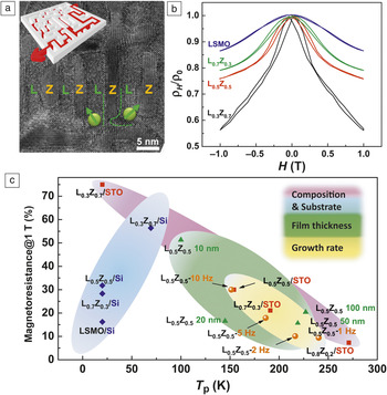
The transmission electron microscopy image in Figure 4 a shows a representative nano-maze spinodal structure in the LSMO-ZnO VAN system, where the insulating ZnO acts as a tunneling barrier, and the semimetallic LSMO is a ferromagnetic electrode with a high degree of spin polarization. Reference Chen, Zhang, Khatkhatay, Su, Tsai, Chen, Jia, MacManus-Driscoll and Wang48 More interestingly, the tunable microstructure in VAN films provides an excellent route for manipulating the corresponding LFMR effects, as illustrated in Figure 4b. The LFMR increases continuously with increased ZnO concentration (below the percolation threshold of 70 mol%), which demonstrates the important role of the tunneling barrier in controlling the overall LFMR effect. Reference Zhang, Chen, Khatkhatay, Tsai, Su, Jiao, Zhang and Wang29 Figure 4c summarizes a number of factors in addition to film composition that actively influence the film microstructure and corresponding magnetotransport effects, including substrate parameters, film thickness, and growth rate. Reference Chen, Bi, Tsai, Lee, Su, Zhang, Jia, MacManus-Driscoll and Wang28,Reference Zhang, Chen, Khatkhatay, Tsai, Su, Jiao, Zhang and Wang29,Reference Chen, Weigand, Bi, Zhang, Lu, Dowden, MacManus-Driscoll, Wang and Jia41,Reference Chen, Zhang, Khatkhatay, Su, Tsai, Chen, Jia, MacManus-Driscoll and Wang48
(a) Plan-view transmission electron microscopy image of a La0.7Sr0.3MnO3 (LSMO)-ZnO vertically aligned nanocomposite (VAN) film showing an alternative arrangement of LSMO (L) and ZnO (Z) phases. Inset: Schematic of this nano-maze structure. (b) Normalized resistivities (ρ H /ρ0) of LSMO-ZnO VAN films with different compositions as a function of magnetic field (H). (c) Summary of maximum magnetoresistance (MR) at 1 T and corresponding peak temperatures (T p) of LSMO-ZnO VAN films with different growth parameters and on Si or SrTiO3 (STO) substrates. (a) Reproduced with permission from Reference 48. © 2013 American Institute of Physics. (b) Reproduced with permission from Reference 29. © 2013 American Chemical Society.

Electric-field-dependent charge transport along interfaces for nonvolatile switching devices
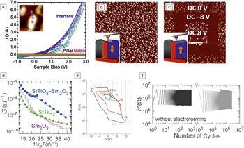
Local electrical or ionic conduction at the vertical interfaces in VAN structures allows for combined electronic and nanoionic effects, with the latter only beginning to emerge as the field of ionitronics. In the well-studied system of BFO-CFO VAN films, robust local electronic conduction has been observed at the vertical interfaces, compared to the insulating characteristics in both the BFO matrix and the CFO nanopillars ( Figure 5a). Reference Hsieh, Liou, Huang, Liang, He, Zhan, Chiu, Chen and Chu30 Oxygen vacancies induced at the vertical interfaces provide mobile charge carriers for local conduction. A further step beyond probing interface conduction has been achieved by reversible and nonvolatile switching of the local conduction at the vertical interfaces (Figure 5b–c) Reference Hsieh, Strelcov, Liou, Shen, Chen, Kalinin and Chu82 through application of an appropriate DC bias with a nanoscale conduction tip.
(a) Current–voltage (I–V) curves measured with a conductive atomic force microscope near and off the vertical interface in BiFeO3-CoFe2O4 (BFO-CFO) vertically aligned nanocomposite films. Inset: Positions where measurements were made. Local conduction current images (b) without electric-field poling and (c) with ±8 V poling. The dark square area shows that the local conduction diminishes under negative bias, indicating a nonvolatile redistribution of oxygen vacancies at the interface. Insets: Schematics showing the electric modulation of the conduction behavior at the interface through the control of oxygen vacancies (P represents the direction of ferroelectric polarization). (d) Conductance (G) of SrTiO3-Sm2O3 (STO-SmO) nanocomposite films measured from 20°C to 550°C. (e) Resistance (R) of nanoscaffold STO-SmO thin-film capacitors as a function of voltage (V) at room temperature. (f) Cyclability measurements of the electroresistance behavior in an STO-SmO nanoscaffold device. (a) Reproduced with permission from Reference 30. © 2012 Wiley-VCH. (b–c) Reproduced with permission from Reference 82. © 2013 American Chemical Society. (d–f) Reproduced with permission from Reference 32. © 2014 Wiley-VCH.

In the SrTiO3-Sm2O3 (STO-SmO) system, both local conduction effects using a nanoscale tip and large-area effects using macroscopic electrodes have been measured. Reference Lee, Sangle, Lu, Chen, Zhang, Lee, Wang, Jia and MacManus-Driscoll32 Enhanced conductance has been demonstrated in the VAN films along interfaces (Figure 5d), and nanoscale vertical conduction paths in the SrTiO3 matrix at the interfaces with the Sm2O3 nanocolumns enabled tunable resistive switching with excellent cyclability and endurance (Figure 5e–f).
An additional benefit of these structures is that there is no need for an initial destructive electroforming process. In this process, nanoscale conductive filaments are formed by applying a soft breakdown electric field, with poor control over uniform, reliable, and scalable device performance. Although the memristive switching phenomenon has been observed in standard thin films of transition metal oxides and complex oxides, Reference Strukov, Snider, Stewart and Williams83–Reference Yang, Pickett, Li, Ohlberg, Stewart and Williams86 it is mostly related to the presence of oxygen vacancies and cation interstitials, and the effective control of such defects is key for highly controlled devices. Reference Yang, Strukov and Stewart87 The VAN structures allow this desired level of control because the vertical ionic channel defects arise from the structural discontinuity between two incompatible phases, that is, oxygen vacancies are induced along vertical heterointerfaces in the self-assembled VAN architectures. Hence, robust, high-endurance memristor devices can be created using VAN films.
Electric-field-dependent electron trapping for charge-coupled magnetoelectric devices
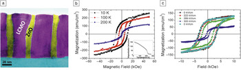
Electrical-field-induced charge modulation at the interface provides an interesting route for the control of magnetism based on VAN architectures. For instance, in La2CoMnO6-ZnO (LCMO-ZnO) VAN films ( Figure 6a), in which LCMO is a ferromagnetic insulator with a critical temperature over 200 K (Figure 6b), reversible electric-field-induced switching of the magnetic properties of LCMO was observed at 120 K (Figure 6c). Reference Fix, Choi, Robinson, Lee, Chen, Prasad, Wang, Blamire and MacManus-Driscoll23 This effect is consistent with charge-mediated coupling between magnetism and an electric field through oxygen vacancies along the vertical interfaces. Applying an electric field to the nanocomposite film produces an electrical current along the vertical interface, at which electrons can be trapped. As a result, the charge state of the oxygen vacancies is altered. This, in turn, modifies the valence state of the cations in LCMO, lowering its critical temperature. The trapping/detrapping of electrons at the vertical interfaces is controlled by the sign and magnitude of the electric field, and hence, the magnetic properties could be modulated accordingly. Both to further understand the interesting phenomena observed in the LCMO-ZnO system and to possibly achieve the “holy grail” of room-temperature operation, new VAN film compositions incorporating magnetic insulating phases with ionic/dielectric phases should be explored.
(a) Cross-sectional transmission electron microscopy image of a La2CoMnO6 (LCMO)-ZnO vertically aligned nanocomposite film. (b) Magnetization curves of a 100-nm-thick LCMO-ZnO film. Inset: Corresponding magnetization versus temperature curve with an in-plane magnetic field of 1000 Oe. (c) Magnetization curves at 120 K for different electric fields applied to a 200-nm-thick LCMO-ZnO film. (a–c) Reproduced with permission from Reference 23. © 2013 American Chemical Society.

Dielectric effects
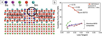
Dielectric studies in VAN structures originate from the effort to fabricate materials with high dielectric tunability and low dielectric loss. The material requirements for tunability and dielectric loss are usually in conflict in conventional methods, such as selective chemical doping and the addition of secondary low-permittivity phases. Reference Cole, Nothwang, Hubbard, Ngo and Ervin88–Reference Kong, Li, Zhang, Zhai, Boey and Ma90 By exploiting novel strain states in VAN structures, a new paradigm to achieve the desired high dielectric tunability that scales inversely with loss (rather than proportionally with it, as in standard composite systems) has been developed. Specifically, Ba0.6Sr0.4TiO3 (BSTO) was grown in heteroepitaxial BSTO-SmO VAN films, where the stiff SmO matrix generates auxetic-like strain states in the BSTO (i.e., under tension both in-plane and out-of-plane) ( Figure 7a). Reference Lee, Harrington, Kursumovic, Defay, Wang, Bi, Tsai, Yan, Jia and MacManus-Driscoll34 As a result, an unprecedented level of dielectric tunability accompanied by low dielectric loss was successfully obtained (Figure 7b), demonstrating the great potential of the VAN design for preparing high-performance radio frequency and microwave device applications.
(a) Schematic drawing showing the vertical strain in Ba0.6Sr0.4TiO3 (BSTO) using the stiffer Sm2O3 (SmO) phase as the matrix. (b) Tunability versus loss tangent for BSTO-SmO vertically aligned nanocomposite films with different film compositions (C and C 0 are the capacitance with and without an electric field, respectively). (a–b) Reproduced with permission from Reference 34. © 2012 American Chemical Society.

Summary, challenges, and future opportunities
We have highlighted several examples of materials with enhanced performance and multifunctional devices based on vertically aligned nano-architectures. The huge interfacial area for functional coupling and the possibility of vertical epitaxial strain control independent of the substrate, as well as self-assembly, provide an entirely new approach to tuning the properties of metal oxides. Research challenges in this area lie firmly in the materials science domain. They encompass materials architectonics (designing and growing the appropriate coupled thin-film nanocomposite structures and tuning their dimensions), materials chemistry (choosing the appropriate compositions to be used and understanding their chemical interactions), and materials physics (understanding the ways in which the materials couple [e.g., through strain or charge] and how this impacts the physical properties).
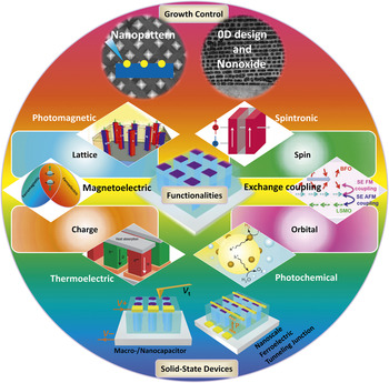
Looking to the future, there is a huge scope for exploring new systems and film designs based on this unique platform. Figure 8 summarizes representative examples, which involve mutual coupling between (ferro)magnetic, (ferro)electric, optical, thermal, and strain effects, so that integrated multifunctionalities can be achieved. Reference Seidel, Luo, Suresha, Nguyen, Lee, Kim, Yang, Pennycook, Pantelides, Scott and Ramesh91–Reference Zhang, Chen, Jian, Zhu, Chen, Lu, Jia, MacManus-Driscoll, Zhang and Wang96 Particularly important goals in these areas include achieving the desired levels of structural, chemical, and electrical perfection and manipulating the fundamental interactions governing the physical properties. In addition to bottom-up approaches to achieve this, namely (pseudo-) spinodal decomposition, nanopatterning could also be implemented to help direct the assembly. Reference Aimon, Choi, Sun, Kim and Ross38,Reference Aimon, Kim, Sun and Ross97,Reference Choi, Aimon, Kim, Sun, Gwyther, Manners and Ross98 In addition, to add further functionality and tunability to the structures, architectonic structures with zero, one, and two dimensions can be explored. Reference Ning, Wang and Zhang99,Reference Li, Wang, Yao, Yang, Wang, Hu, Chen, Sun, Tian, Li, Chen and Viehland100 One further point to note is that, although most experience to date has been with oxide materials, nonoxide materials, with all the additional wide-ranging functionalities they offer, should be explored. Reference Kawasaki, Schultz, Lu, Gossard and Palmstrøm101,Reference Lu, Ouellette, Preu, Watts, Zaks, Burke, Sherwin and Gossard102 Even though much progress has been made in the past 10 years, many avenues remain to be explored, from theory to modeling to growth and, ultimately, to practical device demonstrations in new systems with wide functional possibilities.
Research prospects for multifunctional heteroepitaxial nanocomposite films that can be engineered from growth control to functionalities and solid-state devices. Note: LSMO, La0.7Sr0.3MnO3; BFO, BiFeO3; AFM, antiferromagnetic; FM, ferromagnetic; SE, superexchange. P is the ferroelectric polarization, V t is the tip bias. V + and V – represent the external positive and negative voltage applied on the vertically aligned nanocomposite film, respectively.

Acknowledgments
We gratefully acknowledge support from the US National Science Foundation (DMR-1007969, DMR-1401266, and DMR-0846504). J.L.M.-D. gratefully acknowledges support from the European Research Council (ERC-2009-AdG 247276 NOVOX) and the Leverhulme Trust. R.R. acknowledges continued support from the US Department of Energy and the NSF-TANMS and SRC-FENA programs.