Introduction
Atomic layer deposition (ALD) has experienced rapid growth in the past decade in both scientific research and industrial applications. The number of publications in this field has increased almost exponentially, as has the number of application areas. From the materials point of view, the largest part of the research has been devoted to high dielectric constant (high-κ) oxides aimed at applications in microelectronics. By replacing SiO2 (κ = 3.9) with HfO2 or ZrO2, κ-values of 20–40 can be reached. New ALD thin-film materials have been introduced among metals, especially noble metals, ternary oxides, metal fluorides, and hybrid materials. Materials fabricated by ALD range from single material types to the more recent lithium-containing compounds, tellurides, and selenides.
Puurunen has reviewed all of the ALD processes published before 2005.Reference Puurunen1 The list of ALD materials and processes that are currently available is lengthy but still far from comprehensive. There are many elements and a large number of different types of compounds that have never been deposited using ALD, probably because there has not yet been a need to develop ALD processes for these materials. ALD processes are needed, in general, when the films have to be conformal. Very thin films, nanolaminates, and deposition on nanomaterials are other reasons to employ ALD.Reference Leskelä and Ritala2
In the present review, the focus is on new ALD processes developed during the last 10 years. The focus is specifically on thermal ALD processes, while keeping in mind that plasma-ALD has significantly increased in importance over the past few years. Kessels and Putkonen discuss advances in plasma ALD and related methods in this issue of MRS Bulletin.
High-κ oxides
High permittivity oxide thin films are needed in both complementary metal oxide semiconductor (CMOS) transistors and dynamic random-access memory (DRAM) capacitors to replace silicon oxide. The shrinking of device sizes requires increasing capacitance density without extensively increasing leakage. This can be done using high-κ oxides that can be applied as thicker films than silicon oxide, giving the same capacitance density and low enough leakage current.
The replacement of silicon oxide by hafnium oxide-based high-κ material in CMOS devices in 2008 was a revolutionary development.3 Researchers were able to continue shrinking device dimensions in accordance with Moore’s law. Also in the case of DRAMs, the development has been rapid. The architecture of DRAMs changed in the 1990s from two-dimensional to three-dimensional stacked or trench capacitor structures, and when high-κ oxides came into the picture, ALD was needed in film deposition. Currently, the capacitance equivalent thickness (CET) requirement in DRAMs for the oxide film is below 1 nm and will decrease to 0.5 nm in the near future, while keeping the leakage current density below 10–7 A/cm2 at 1 V.4 At the moment, the most widely used dielectric material in DRAMs is an ALD-formed ZrO2-Al2O3-ZrO2 nanolaminate.Reference Kuesters, Beug, Schroeder, Nagel, Bewersdorff, Dallmann, Jakschik, Knoefler, Kudelka, Ludwig, Manger, Mueller and Tilke5
The transition of ALD high-κ oxides to the product level required extensive research and development, including the analysis of a wide range of precursor materials and processes. Most of the attention has been devoted to hafnium and zirconium oxides, but rare-earth metal oxides and other doping systems have also been studied. In DRAM studies, zirconium and hafnium oxides have been the most popular materials, but titanium dioxide has also received attention.
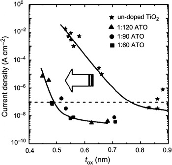
TiO2 is an interesting high-κ material because of its high dielectric constant, which varies from 40 to 160 depending on the phase. Several ALD processes have been developed for TiO2 films,Reference Puurunen, Sajavaara, Santala, Miikkulainen, Laitinen and Leskelä6 but the problem is the high leakage currents in these films. Researchers have tried to improve the situation by doping or using nanolaminates where the TiO2 layer is sandwiched between oxides that leak less, for example Al2O3 and HfO2. TiO2 films grown at low temperatures (<300°C) from different precursors (chlorides, alkoxides, alkylamides) crystallize in the anatase structure.Reference Puurunen, Sajavaara, Santala, Miikkulainen, Laitinen and Leskelä6 However, the high dielectric constant rutile structure is the more desired polymorph. The formation of the rutile phase can be enhanced by an underlayer, and recent reports have shown that a rutile structured RuO2 electrode promotes the rutile phase of TiO2.Reference Fröhlich, Tapajna, Rosova, Dobrocka, Husekova, Aarik and Aidla7 High-κ values (155) and low CET values (<0.5 nm) have been reported for RuO2/TiO2 devices. The leakage problem still exists, but Kim et al. solved that through aluminum doping.Reference Kim, Choi, Lee, Seo, Lee, Han, Ahn, Han and Hwang8 When 8% Al is homogeneously doped into rutile TiO2, the leakage currents can be lowered by several orders of magnitude (Figure 1).
Leak current density at 0.8 V versus capacitance equivalent thickness (t ox) for TiO2 and TiO2:Al films with different cycle ratios (1:60, 1:90, 1:120). The dashed line shows the acceptable leakage current level (10–7 A/cm2).Reference Kim, Choi, Lee, Seo, Lee, Han, Ahn, Han and Hwang8 ATO, aluminum-doped TiO2. Reprinted with permission. © 2008, Wiley.

The ALD high-κ oxide studies were first focused on HfO2 films and hafnium oxide-based materials, and these materials were subsequently employed in Intel’s transistors.3 Hafnium was preferred over zirconium since it is more stable with polysilicon, which was used as the gate electrode material in transistors. This requirement is no longer relevant because metal gates have replaced polysilicon as the material of choice. In addition, the fabrication of a phase pure material was easier with HfO2 than ZrO2, both of which have several different crystal structures. Especially in DRAM applications, ZrO2 has become more important than HfO2 since the cubic and tetragonal phases of ZrO2 show higher κ values (40) than the corresponding HfO2 phases (30). The monoclinic phases of both oxides have κ values around 20.
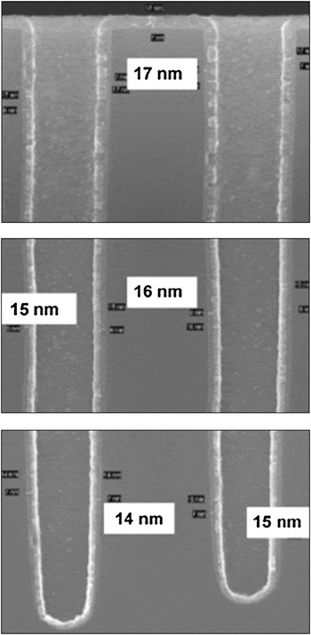
The first and still used HfO2 ALD process is based on hafnium chloride and water. During the last 10 years, several new precursors and processes have been developed. The precursors include alkylamides, amidinates, alkoxides, cyclopentadienyls, and heteroleptic, mixed ligand complexes of these four precursors.Reference Niinistö, Kukli, Heikkilä, Ritala and Leskelä9 In most cases, water or ozone can be used as the oxygen source. Except for cyclopentadienyl compounds, limited thermal stability is typical for the complexes containing organic ligands, which sets the maximum deposition temperature to 300°C. Higher deposition temperatures are often beneficial for achieving purer films and the desired crystalline phase. The alkylamides are very reactive toward water and ozone, resulting in low impurity oxide films with high κ-value, but, on the other hand, they suffer from thermal instability at 300°C. The process using Zr(NEtMe)4 (Et = ethyl, Me = methyl) and ozone at 275°C has yielded, on TiN electrodes, a κ value close to 40 and a CET value of 0.8 nm.Reference Kim and Hwang10 In the presence of the high-κ phase, similar CET values and low leakage currents have been reported for mixed ligand CpZr(NMe2)3 (Cp = cyclopentadienyl).Reference Niinistö, Kukli, Kariniemi, Ritala, Leskelä, Blasco, Pinchart, Lachaud, Laaroussi, Wang and Dussarrat11 Cyclopentadienyl compounds are versatile precursors enabling tailoring of the properties by substitutions in the five-membered ring. The Cp precursors show good thermal stability and moderate growth rates but result in mixed crystallographic phases of HfO2 and ZrO2. Recent results on (CpR)M(NMe2)3 (R = alkyl group, M = Zr, Hf) mixed ligand compounds show the beneficial properties of both corresponding homoleptic compounds (one type of ligand is bound to the metal ion): good thermal stability, reactivity and growth rate, enhanced formation of high-κ phases, and good conformability of the films (Figure 2).Reference Niinistö, Kukli, Kariniemi, Ritala, Leskelä, Blasco, Pinchart, Lachaud, Laaroussi, Wang and Dussarrat11
Cross-sectional scanning election microscopy images of a ZrO2 film grown by the CpZr(NMe2)3/O3 process at 275°C into 60:1 aspect ratio trenches. The upper image shows the top part of the trench, and those below are the middle and bottom parts. The trench opening is 115 nm wide with a depth of 6.75 mm. Labels denote the ZrO2 film thicknesses.Reference Niinistö, Kukli, Kariniemi, Ritala, Leskelä, Blasco, Pinchart, Lachaud, Laaroussi, Wang and Dussarrat11 Cp = cyclopentadienyl; Me = methyl. Reprinted with permission. © 2008, Royal Chemical Society.

The concern with ZrO2 was the formation of the monoclinic phase and stabilization of the high-κ phases. It seems that it is possible to affect the structure by precursor selection. The other well-known method is doping. Yttrium-stabilized zirconia and hafnia have the cubic/tetragonal structure.Reference Niinistö, Mäntymäki, Kukli, Costelle, Puukilainen, Ritala and Leskelä12 Theoretical predictions indicate that ions with a smaller ionic radius than Zr or Hf favor the stabilization of the tetragonal phase, and ions with larger ionic radius favor the cubic form.Reference Lee, Cho, Lee, Hwang and Han13 It has been experimentally verified that doping of ALD ZrO2 and HfO2 with 5–8 cation-% rare earth ions results in films with the cubic/tetragonal phase.Reference Niinistö, Kukli, Heikkilä, Ritala and Leskelä9
Ternary oxides
The number of ternary and quaternary oxides studied within ALD is limited but increasing. Interest in the multicomponent oxides stems from their favorable electrical, ferroelectric, or magnetic properties. There are several ways ternary compounds can be processed: (1) mixing of binary oxide deposition cycles, (2) use of bimetallic precursors, and (3) use of precursors that introduce two of the three elements into the film. The mixing of binary oxide processes to get the right stoichiometry is quite straightforward, but the optimum process temperatures may be different in the binary processes, making the temperature window for the ternary processes narrow.Reference Vehkamäki, Hatanpää, Ritala and Leskelä14 The growth rate can also be different on the binary oxide itself rather than on the other oxide. This effect can even be beneficial, as has been seen in the case of SrTiO3 and BaTiO3, where the growth of the reactive binaries SrO and BaO is challenging, but the growth of the ternaries is easier.
The use of bimetallic single-source precursors is common in chemical vapor deposition (CVD) but has been very rarely investigated for ALD. The most well-known case is the deposition of SrTa2O6 from SrTa2(OEt)10dmae2 (dmae = dimethylaminoethoxide) and water.Reference Vehkamäki, Ritala, Leskelä, Jones, Davies, Sajavaara and Rauhala15 The reason for the limited use of bimetallic precursors is the lack of volatile, thermally stable, and reactive compounds. The third way to deposit ternary compounds is the use of a reactant that supplies two of the three elements into the film, for example, in the case of silicates, where reactions between metal chlorides and silicon alkoxides produce metal silicates.Reference Ritala, Kukli, Rahtu, Räisänen, Leskelä, Sajavaara and Keinonen16
The number of quaternary oxide films made by ALD is very small. In the deposition of ferroelectric SrBi2Ta2O9, the bimetallic SrTa2(OEt)10dmae2 has been used together with a bismuth precursor.Reference Vehkamäki, Hatanpää, Kemell, Ritala and Leskelä17 Three metal precursors and a separate oxygen precursor have been successfully used in the case of Bi-Ti-Si-O films.Reference Hwang, Kim, Hwang, Min and Cho18 Maintaining the right stoichiometry in deep trenches is a challenge. With quaternary compounds, the temperature window can be even narrower than with ternary compounds. Liquid injection ALD, where the precursor solution is injected in a vaporization chamber and further into the reactor, can then be useful, and introduction of quaternary precursor mixtures has been successfully employed in oxide depositions.Reference Min, Cho, Aslanov, Han, Kim and Hwang19
The first ALD ternary oxides were deposited in the 1990s, targeting magnetic oxides. These transition metals containing compounds (LaCoO3, LaNiO3) were made using thd-chelates (thd = 2,2,6,6-tetramethyl-3,5-heptanedione) and ozone as precursors.Reference Seim, Mölsä, Nieminen, Fjellvåg and Niinistö20 The other common feature in ALD of ternary oxides is the amorphous structures in the as-deposited state. Annealing is needed to get crystalline films with the desired magnetic and electric properties.
Further interest in ternary oxides came from applications to DRAMs, where a shift away from SiO2 to binary high-κ oxides or more preferably to very high-κ materials such as titanates started early in the 2000s. SrTiO3 has attracted consistent interest as a possible material for DRAM capacitors. The limited Sr precursor chemistry has slowed the industrial use of ALD of SrTiO3. The oldest and still most commonly used chemistry is based on Sr cyclopentadienyls.Reference Vehkamäki, Hatanpää, Hänninen, Ritala and Leskelä21 Mixed rare-earth oxides form a third type of ternary oxides receiving attention as possible candidates for high-κ materials in microelectronics. The combination of large rare-earth ions with small ones can produce separate ternary compounds with a perovskite structure, such as LaLuO3 and GdScO3.
Yet another ternary oxide material type is formed by ferroelectrics. The earlier mentioned quaternary compound SrBi2Ta2O9 is an interesting ferroelectric material. From ternaries, BaTiO3 is a well-known ferroelectric material, and it was made by ALD over a decade ago.Reference Vehkamäki, Hatanpää, Hänninen, Ritala and Leskelä21 Bismuth titanates, Bi4Ti3O12, form another group of ferroelectric materials ALD. In this case, the precursor chemistry of bismuth has played a critical role, and so far the most versatile precursor has been Bi(OCMe2iPr)3 (i = iso).Reference Hatanpää, Vehkamäki, Ritala and Leskelä22 Lead-containing ternary compounds are interesting due to their applications in sensors and as lead zirconate titanate ferroelectrics. PbZrO3 films have been grown using Ph4Pb, Zr(thd)4 and ozone at around 300°C.Reference Harjunoja, Väyrynen, Putkonen, Niinistö and Rauhala23
Ternary oxide films are usually deposited at low temperatures because of the low thermal stability of the precursors. Crystalline films are obtained after high temperature annealing. In many cases, it would be beneficial to get crystalline films directly in the as-deposited state, as has been done, for example, by selecting a strontium precursor that is stable at higher temperatures, allowing crystalline SrTiO3 films to be deposited at 370°C.Reference Lee, Kwon, Han and Hwang24
Metals
Tungsten and molybdenum were two of the first metals deposited by ALD. Their process follows the ALD principle of exchange reaction type. The reaction involves reduction of WF6 (MoF6) by silanes and boranes.Reference Klaus, Ferro and George25 The reaction mechanism explains the high growth rate (2.5 Å/cycle) through alternating W-SiHyFz and W-WFx surfaces. This fluorosilane elimination reaction is thermodynamically favorable and results in high and complete reactivity.
Copper has been one of the most desired ALD metals, but its deposition is very challenging. As reviewed by Kim in 2003,Reference Kim26 no process was available for application at that time. Processes where metals are fabricated via an oxide route (i.e., first an oxide is made with water or ozone, and then the oxide is reduced to metal with H2) have been reported for copper and nickel.Reference Soininen, Elers, Saanila, Kaipio, Sajavaara and Haukka27 The discovery of amidinate precursors (an amidinate salt has the general structure M+[RNRCNR]– where R is an alkyl group) was also a significant step forward in ALD copper chemistry.Reference Lim, Rahtu and Gordon28 The direct reduction of Cu precursors with hydrogen has not been possible, but amidinates perform better in this sense. However, the ALD Cu problem is not completely solved, and new processes are being studied, such as those reducing Cu dimethylamino-propoxide with diethyl zinc at 100–120°CReference Lee, Hwang, Nam, Lee, Kim, Koo, Baunemann, Fischer and Sung29 and catalyzing the hydrogen reduction of Cu(hfac)2 (hfac = hexafluoroacetylacetonate) by pyridine at room temperature.Reference Kang, Yun and Chang30
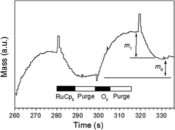
Noble metal ALD, first reported in 2003, has been a success story. With thermal ALD, all platinum group noble metals (Ru, Rh, Pd, Os, Ir, Pt) have been deposited using O2 as the other precursor, together with metal-organic and organometallic compounds.Reference Aaltonen, Alén, Ritala and Leskelä31 With platinum-group noble metals, this oxidative process is possible because of their strong tendency to form metal films instead of oxides. Oxygen, as the other reactant, reinforces this preference for forming metal, and the main mechanism in the process is combustion of the hydrocarbons of the ligands by oxygen, though some exchange reactions may take place too. Metals themselves activate the otherwise quite inert O2 molecule by dissociating it to atomic oxygen. Noble metal processes have been studied in situ using quartz crystal microbalance and quadrupole mass spectroscopy measurements (the quartz crystal microbalance measures the weight gain on the substrate after each ALD cycle, and the quadrupole mass spectrometry records the gaseous reaction products released from the growth process), and the reaction mechanisms are rather well understood (Figure 3).Reference Aaltonen, Arstila, Ritala and Leskelä32 This kind of process has been developed for Ru, Rh, Pd, Ir, Os, and Pt. When ozone is used instead of oxygen, noble metal oxides can be deposited at low temperatures (< 200°C), but at higher temperatures, this process also produces metal films.Reference Hämäläinen, Munnik, Ritala and Leskelä33 The processes with a pulsing sequence of MLn–O3–H2 (ML = metal-ligand) produce metal films already below 200°C.Reference Hämäläinen, Puukilainen, Kemell, Costelle, Ritala and Leskelä34 The nucleation of noble metal films on oxide surfaces is a problem, since a long incubation time is usually needed. Relatively thick films (5 nm) are needed to obtain continuous, well conducting layers. The incubation time depends on both substrate surface and the ruthenium precursor. Even the structure of the substrate may have an effect, as seen in the case of TiO2, where Ru films showed a slightly shorter incubation time on anatase than on rutile or amorphous surfaces.Reference Kim, Han, Han and Hwang35 The use of noble metal oxide as the growth initiator layer and reduction of the oxide to metal could improve the situation, as shown with Pt and Ir films.Reference Hämäläinen, Munnik, Ritala and Leskelä33, Reference Hämäläinen, Puukilainen, Kemell, Costelle, Ritala and Leskelä34
Quartz crystal microbalance data measured during the reaction cycles for RuCp2 and O2. m 0 denotes the total mass change during one complete reaction cycle, and m 1 denotes the mass change during the RuCp2 pulse. Note that the mass increases during the O2 pulse and decreases during RuCp2 pulse, indicating adsorption of excess oxygen onto the surface.Reference Aaltonen, Arstila, Ritala and Leskelä32 Reprinted with permission. © 2005, Electrochemical Society.

Only a few processes have been developed for the first row transition metals (Fe, Co, Ni, Cu). Those based on amidinate precursors rely on H2 reduction chemistry.Reference Lim, Rahtu and Gordon28 The growth rates in these processes vary, indicating that the surface chemistry is not favorable in all cases. The electropositive metals (Al, Ti, Ta) are of interest not only because they are conductive, but also because they can be used as adhesion layers and barrier layers in Cu interconnects. Thermal ALD of these electropositive metals would require conditions that are not possible with the existing reactors. Therefore it was necessary to use hydrogen plasma in their deposition.Reference Kim26 The extreme oxygen sensitivity of these metals makes their ALD very challenging, however.
Silver and gold are important metals, not only because of their low resistivity but also due to their catalytic and optical properties. The surface plasmon properties of silver have recently received much attention. Only two reports have been published on silver ALD, and both of them are based on the hydrogen radical-enhanced reduction of (2,2-dimethylpropionato)silver(I)triphenylphosphineReference Niskanen, Hatanpää, Arstila, Leskelä and Ritala36 or Ag(fod)(PEt3) (fod = 2,2,-dimethyl-6,6,7,7,8,8,8-heptafluoro-3,5-octanedionato).Reference Kariniemi, Niinistö, Hatanpää, Kemell, Sajavaara, Ritala and Leskelä37
Fluorides
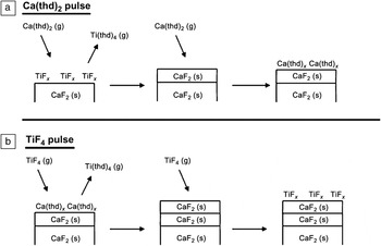
ALD of halide films has focused on fluorides, since fluorides are stable and non-hygroscopic and have interesting optical properties, with only one paper on chlorides. The chloride work focused on the growth of CuCl nanoparticles from [bis(trimethylsilyl)acetylene]-(hexafluoroacetylacetonato)copper(I) and hydrogen chloride.Reference Natrajan, Maydannik, Cameron, Akopyan and Novikov38 The first fluoride process developed was based on HF, which was obtained by the thermal decomposition of NH4F. The more recent studies exploit volatile metal fluorides (TiF4, TaF5) as fluorine precursors. They react with β-diketonato complexes of alkaline earth and rare earth metals to form stable solid fluorides (CaF2, MgF2, LaF3, and YF3).Reference Pilvi, Arstila, Leskelä and Ritala39, Reference Pilvi, Puukilainen, Kressig, Leskelä and Ritala40 These exchange reactions produce pure fluoride films with only about 1% Ti or Ta impurities (Figure 4). The quality of the films is high enough for optic applications, but better transmittance in the UV region would be desirable. The use of organic or fluorine-containing ligands is one way to obtain fluoride films, as exemplified by the work of Putkonen with CaF2.Reference Putkonen41
Suggested reaction schemes for CaF2 atomic layer deposition (ALD) during the (a) Ca(thd)2 pulse and (b) TiF4 pulse.Reference Pilvi, Arstila, Leskelä and Ritala39 Note: thd, = 2,2,6,6-tetramethyl-3,5-heptanedione. The incoming Ca(thd)2 reacts with the TiFx terminated surface forming CaF2 on the substrate and Ti(thd)4 vapor. When the Ca(thd)2 dose is high enough, it forms a Ca(thd)x terminated surface. In the next step, the incoming TiF4 reacts with the Ca(thd)x terminated surface and also forms solid CaF2 and Ti(thd)4 vapor. A high TiF4 dose saturates the surface, leaving TiFx surface groups, and the cycle can start again. Reprinted with permission. © 2007, American Chemical Society.

Li compounds
Alkali metals containing thin films have been studied very little in ALD because they have not been needed for ALD applications. Lithium compounds are, at the moment, the most interesting due to their need in Li-ion batteries. The designs of all solid-state 3D structure batteries show features that make the use of ALD relevant. In 3D structures, all the components—electrodes, barrier layers, and electrolyte—need to be conformal thin films. In all solid-state structures, the electrolyte is also solid and probably should be made by ALD. Therefore increased research activities are ongoing to develop processes for Li-containing materials usable in batteries.
Li precursors have been synthesized and studied in ALD reactions. The Li(thd) and ozone process produces lithium carbonate,Reference Putkonen, Aaltonen, Alnes, Sajavaara, Nilsen and Fjellvåg42 whereas the films obtained from lithium tert-butoxide (LitOBu) and water were either oxide or hydroxide. Experiments for pure lithium oxide have not been successful, but the previously mentioned lithium precursors can be used for ternary or quaternary compounds, as shown with lithium lantanate and lithium lanthanum titanate.Reference Aaltonen, Alnes, Nilsen, Costelle and Fjellvåg43 Recently, lithium phosphate and silicate films also have been deposited.Reference Hämäläinen, Hatanpää, Holopainen, Munnik, Ritala and Leskelä44 The precursors were trimethylphosphate (TMP) and either Li(N(SiMe3))2 or LiOtBu for the phosphate, and lithium bis(trimethylsilyl)amide (LiN(SiMe3)2) and ozone for the silicate.
Selenides/tellurides and antimonides
Telluride films have been grown by ALD since the 1980s using an element as the precursor. The metal precursors used were elemental as well, which is possible with group 12 metals (Zn, Cd, Hg). The interest toward these telluride films came from their use in thin-film solar cells. For other metal chalcogenides, H2Se and H2Te are possible precursors, but their toxicity is of significant concern, and they cannot be used in a normal laboratory environment.
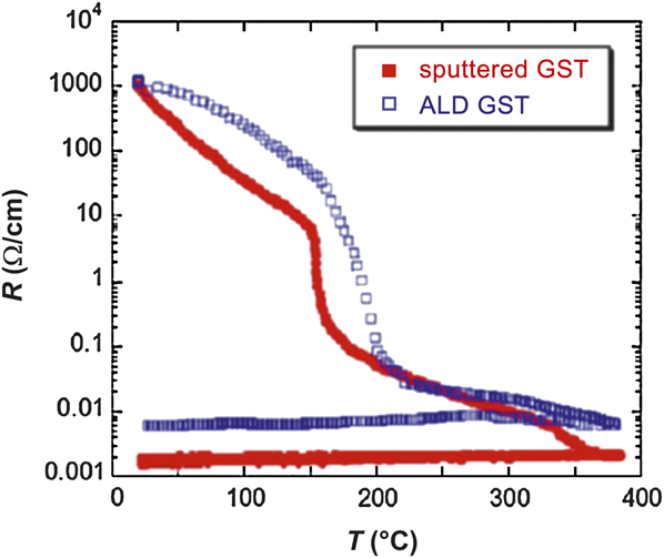
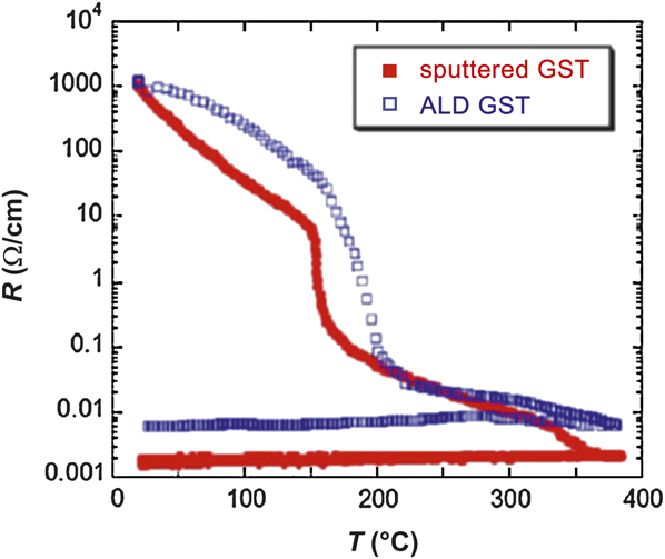
Recently, ALD of tellurides and selenides using alkylsilyls of tellurium and selenium and various metal halides as precursors has been reported.Reference Pore, Hatanpää, Ritala and Leskelä45 This chemistry was found to work at very low temperatures (i.e., below 100ºC), and this was explained in terms of the favorable formation of alkylsilyl halides as volatile by-products. The motivation for the telluride films was fabrication of germanium antimony tellurides for phase change memory (PCM), where information is not stored as electrons but as different resistive states. PCM uses the reversible phase change between the conductive crystalline state and less-conductive amorphous phase (Figure 5).Reference Ritala, Pore, Hatanpää, Heikkilä, Leskelä, Mizohata, Schrott, Raoux and Rossnagel46 The ternary Ge2Sb2Te5 has been the most interesting PCM material, but the binary tellurides SbTex and GeTe have also gained attention as phase change materials.Reference Wuttig and Yamada47
Resistivity (R) versus temperature (T) data for Ge-Sb-Te (GST) films made by atomic layer deposition (ALD) (open boxes) and sputtering (closed boxes) showing very similar behavior.Reference Ritala, Pore, Hatanpää, Heikkilä, Leskelä, Mizohata, Schrott, Raoux and Rossnagel46 Reprinted with permission. © 2009, Elsevier.
The reaction between alkylsilyl compounds and chlorides also can be exploited for elemental antimony that was deposited by the dehalosilylation reaction between (Et3Si)3Sb and SbC13.Reference Pore, Knapas, Hatanpää, Sarnet, Kemell, Ritala, Leskelä and Mizohata48 For the first time, an element other than a metal was deposited by ALD (Figure 6). Pure and conformal thin films of elemental antimony were prepared by thermal ALD. In situ reaction mechanism studies showed that the dehalosilylation reactions are very efficient in eliminating the ligands from the growing surface. Various antimony compounds, such as GeSb, Sb2Te, GaSb, and AlSb, can also be deposited by reacting (Et3Si)3Sb with other metal halides or mixing Sb growth cycles with other ALD processes.
Conformability of the SbCl3-(Et3Si)3Sb atomic layer deposition (ALD) process. (a) Cross-section field-emission scanning electron microscope (FESEM) image of a Sb film deposited on a high-aspect-ratio trench structure. (b)–(d) FESEM images of Sb nanotubes prepared using a porous alumina membrane as a template. The deposition temperature was 100°C, and the number of ALD cycles was 1000. Pulse/purge times were 2/10 s for SbCl3 and 4/10 s for (Et3Si)3Sb.Reference Wuttig and Yamada47 Et = ethyl. Reprinted with permission. © 2011, American Chemical Society.

Organics and hybrid organic-inorganics
Deposition of organic polymers was demonstrated in 1991 by the formation of a polyimide based on sequential reactions between the bifunctional acetic anhydride, pyromellitic dianhydride, PMDA (1,2,3,5-benzenetetracarboxylic anhydride) and the diamines 2,4-diaminonitrobenzene or 4,4’diaminodiphenyl.Reference Yoshimura, Tatsuura and Sotoyama49 This work also coined the terminology MLD (molecular layer deposition) as a subgroup of ALD, emphasizing that the film is built using molecular entities for each growth step.
This demonstration was later expanded to include combinations of other types of functional groups used in polymerization processes, such as reactions between amines and anhydrides for the formation of imides,Reference Yoshimura, Tatsuura and Sotoyama49–Reference Yoshida, Ono and Esashi52 acyl chlorides for the formation of amides,Reference Du and George53, Reference Adamczyk, Dameron and George54 aldehydes for the formation of imines,Reference Yoshimura and Tetsuzo55 isocyanates for the formation of urea,Reference Loscutoff, Zhou, Clendenning and Bent56, Reference Zhou and Bent57 and isothiocyanates for the formation of thiourea.Reference Loscutoff, Lee and Bent58 These processes have also been performed with heterofunctional molecules forming more complex copolymers.Reference Sabapathy and Crooks59 The mentioned reactions rely on the formation of bonds between polar functional groups. A novel alternative reaction mechanism has also been suggested for the formation of covalent non-polar linkages by utilizing UV-induced thiolene reactions.Reference Li, Wang and Buriak60
One challenge with the deposition of polymer materials is the low vapor pressure of most organic compounds and also their limited thermal stability. When this is combined with a limited reactivity, rather long pulsing times may be necessary for obtaining saturated growth. However, when compared to the growth of inorganic compounds, the absolute growth rate is relatively high due to the size of the molecules being included into the film for each step.
The scientific field of polymer material deposition by MLD is still mainly focused on the demonstration of the chemistry involved in the deposition of the different polymers. However, various applications have been investigated, such as polyimides for resistive switching,Reference Yoshida, Ono and Esashi52 multilayered structures combining polymers and inorganic materials for significant reduction in leakage current,Reference Salmi, Puukilainen, Vehkamaeki, Heikkilae and Ritala50 and new novel types of deposition of photoresist material for deep UV lithography.Reference Zhou and Bent57 These studies also prove the strong benefit of using ALD/MLD for deposition of thin films of polymers due to its impressive uniformity, which is not obtainable in an efficient manner by alternative techniques.Reference Yoshida, Ono and Esashi52, Reference Zhou and Bent57
The reaction scheme described for production of polymers can be extended by using metals as connections between organic linkers in formation of compounds resembling metal organic frameworks (MOF), here termed as organic-inorganic hybrid materials. The layout for such reactions was described in 2006,Reference Nilsen and Fjellvåg61 with examples from growth utilizing reactive inorganic precursors such as TMA (trimethylaluminum), DEZ (di-ethyl zinc), ZrCl4, and TiCl4, and organic molecules containing functional groups as alcohols, carboxylic acids, amines, and thiols, among others. See also the review in Reference 62. By utilizing such highly reactive inorganic precursors as connections, a wide range of functional groups on organic compounds can be used with a reactivity enabling fast and efficient processes.
Alcohols are commonly used as functional groups forming metal cones thought to have alkoxide structures resembling those in silicone. In this manner, it is alucone materials when reacted with TMAReference Dameron, Seghete, Burton, Davidson, Cavanagh, Bertrand and George63, Reference Miller, Foster, Zhang, Jen, Bertrand, Lu, Seghete, O’Patchen, Yang and Lee64 and similar zincone materials when reacted with DEZ.Reference Cho, Han, Kim and Sung65, Reference Peng, Gong, VanGundy and Parsons66 The alucones are susceptible to reactions with moisture in ambient air, most probably due to limited saturation of the coordination sphere of the metal.
The alucones have been used for deactivation of photocatalytically active TiO2Reference Liang and Weimer67 and formation of porous surfaces.Reference Liang, Xinhua, Yu, Li, Jiang and Weimer68 The alucones have also been demonstrated as successful sacrificial layers in the formation of air gaps in nanoelectromechanical systems.Reference Seghete, Davidson, Hall, Chang, Bright and George69 The film is barely removed in dry-etch processes but is easily removed in acidic wet etches.
The stability in air of the organic-inorganic films is greatly enhanced when the alcohols are replaced with carboxylic acids, probably due to a more complete saturation of the coordination sphere of the metal by the carboxylic acids,Reference Klepper, Nilsen, Hansen and Fjellvåg70, Reference Klepper, Nilsen and Fjellvåg71 providing relatively hydrophobic surfaces.
Amines can also be used as functional groups with great success, especially when reacted with titanium, such as TiCl4. This has, among others, been demonstrated in Reference Reference Sood, Sundberg, Malm and Karppinen72 with the formation of a stable material when combined with 4,4’diaminodiphenyl.
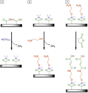
A possible inhibiting step in the formation of such hybrid materials is multiple reactions with the surface by the bifunctional organic linkers. This is especially the case for homofunctional organic linkers with flexible structure such as alkanes. Such effects may be overcome using precursors with protected groups or which must be activated on the surface before subsequent reactions, or simply by exploiting different reactivities in heterofunctional organic linkers. Multiple suggestions are given in Reference Reference George, Yoon and Dameron62, and a three-step (ABC) growth process using a sequence of TMA, ethanolamine, and maleic anhydride has been demonstrated in Reference Reference Yoon, Seghete, Cavanagh and George73 (see also Figure 7).
Schematic of a three-step (ABC) growth process for the deposition of an organic-inorganic hybrid material using a sequence of (a) trimethylaluminum, (b) ethanolamine, and (c) maleic anhydride, where an imide bond also forms.Reference Yoon, Seghete, Cavanagh and George73 Reprinted with permission. © 2009, American Chemical Society.

Similar surface-activated growth preventing multiple reactions with the surface has been demonstrated in References Reference Park, Han, Lee, Cho, Lee, Im and Sung74–Reference Lee, Ryu, Choi, Lee, Im and Sung76 using self-assembled monolayers based on 7-octenylthrichlorosilane. The monolayer is terminated by an alkene group that is converted into the more reactive carboxylic acid by reaction with ozone. This process has been combined with layers of ZnO material to form an n-type semiconductorReference Park, Han, Lee, Cho, Lee, Im and Sung74 and thin-film transistor,Reference Lee, Im, Lee, Im and Sung75 and combined with layers of TiO2 to form a long-term stable resistive switching material.Reference Lee, Ryu, Choi, Lee, Im and Sung76
Subsequent polymerization of the organic linker has also been demonstrated for functionalizing the material.Reference Cho, Han, Kim and Sung65 A film based on DEZ and hexadiyne diol was formed containing alkyne bonds in close proximity. These were subsequently polymerized by UV irradiation to form a zinc oxide cross-linked polymer showing n-type semiconductivity with enhanced carrier mobility.
The possibilities within hybrid structures are plentiful, and prospects for scale-up are good given the enhanced growth rates of these materials. So far for as-deposited films, it has not been possible to reproduce the porosity or crystallinity of the MOF structures, which most closely resemble bulk materials. However, the amorphous films represent a new class of material where the properties are yet barely revealed.
Conclusions
There is a constant need for thin and conformal films of new materials in various applications, and this gives motivation for atomic layer deposition (ALD) research. Developments in ALD have been rapid during the last 10 years. ALD applications expand in two ways: introducing existing ALD processes into new areas and developing new processes for existing and new areas. During the last decade, new processes have been developed for metals, fluorides, chalcogenides, and polymers, and many new elements have been introduced in ALD films. A new class of organic-inorganic hybrid materials has been realized by the ALD technique, opening up unexplored areas.
ALD applications have expanded from microelectronics to protective coatings, and it can be predicted that areas such as optics, solar cells, and microelectromechanical systems will be important in the near future. However, new materials and processes are still needed in microelectronics, as can be seen in the International Technology Roadmap for Semiconductors.4 While this article has focused primarily on thermal ALD and molecular layer deposition processes, there is a strong need to develop plasma-enhanced ALD and other related processes, as described in other articles in this issue.