Introduction
Sunlight is the most abundant, renewable, and non-polluting energy resource available. However, major challenges are harvesting and storing the solar energy in a cost-effective and environmentally friendly manner. Photovoltaic technologies are promising for renewable energy applications, since solar cells are able to convert light directly into electricity. 1 Unfortunately, even though the cost of solar panels and solar electricity has dropped to unprecedented levels, it is still not low enough to compete with traditional fossil fuels and other renewable energy technologies. The key to affordable solar technologies is to develop transformational techniques that offer both high photovoltaic performance and low cost. Reference Turner2
Though silicon-based solar panels are the most used, thin-film solar cells have become more popular recently due to their lower cost and lower energy consumption for manufacturing. Yet the efficiency of thin-film solar cells lags behind that of silicon, making them less competitive. 3 Currently, single-crystal silicon solar cells provide the best power-conversion efficiency (PCE) for solar cells, reaching ∼25% in labs and ∼16–20% from large-scale solar panels. Representative thin-film photovoltaic technology reaches 20% PCE and averages 15% for solar panel products, making it only a supplement to silicon. To promote the cost-effectiveness of thin-film solar cells, the efficiency needs to be boosted to higher levels, while simultaneously reducing cost.
Recently, the family of organic–inorganic perovskite materials (e.g., CH3NH3PbX3, where X = I, Cl, or Br) has taken center stage in this field, with PCE values exceeding 20% in the laboratory and expected low manufacturing cost due to their compatibility with a number of scalable deposition methods. Reference Snaith4–Reference Chen, De Marco, Yang, Song, Chen, Zhao, Hong, Zhou and Yang8 The 20% PCE is even more exciting considering that the first perovskite solar cells were reported in 2009, with demonstrated PCE values around 3.8%. Reference Kojima, Teshima, Shirai and Miyasaka9 All the components of perovskite solar cells can be directly deposited from inexpensive and scalable solution-based approaches, strengthening the position of perovskite-based photovoltaics as promising candidates for low-cost and high-performance solar cells.
The original designs of perovskite solar cells can be traced back to the classical architecture of dye-sensitized solar cells, with organic–inorganic compounds infiltrated into a mesoporous TiO2 structure. Reference Im, Lee, Lee, Park and Park10,Reference Kim, Lee, Im, Lee, Moehl, Marchioro, Moon, Humphry-Baker, Yum, Moser, Gratzel and Park11 Later progress demonstrated that a simpler geometry, a perovskite layer sandwiched between a compact thin film of TiO2 and a hole-conducting organic compound, delivered the highest efficiencies, provided that a uniform and dense morphology was achieved in each of the deposited layers. Reference Jeng, Chiang, Lee, Peng, Guo, Chen and Wen12–Reference Liu and Kelly15 Meanwhile, perovskite absorbers have been shown to play a versatile role in power generation, providing a means for light absorption and charge transport within the same polycrystalline device layer. Reference Lee, Teuscher, Miyasaka, Murakami and Snaith16,Reference Malinkiewicz, Yella, Lee, Espallargas, Graetzel, Nazeeruddin and Bolink17 Such a rapid progress in the design and processing of hybrid perovskites is unprecedented in the field of photovoltaic research. Perovskites have shown remarkable optoelectronic properties, including optimum absorption with a sharp band edge, long charge-carrier diffusion lengths (>1 μm) relative to the absorption depth of incident light (∼several hundred nm), and a high tolerance of structural defects. Reference Yin, Shi and Yan18,Reference Yin, Shi and Yan19
Film formation ability of perovskites, which leads to better film uniformity and larger crystalline domains, appears to be the most crucial parameter to enable the most significant improvements in PCE. Different methods for film formation and the roles of the solvent and precursors have been clearly highlighted for the material properties that are essential for high-efficiency operation of solar cells. Reference Chen, Zhou, Hong, Luo, Duan, Wang, Liu, Li and Yang13,Reference Liu, Johnston and Snaith14,Reference Burschka, Pellet, Moon, Humphry-Baker, Gao, Nazeeruddin and Gratzel20–Reference Leyden, Ono, Raga, Kato, Wang and Qi29 In this review, we focus on understanding a very promising perovskite processing method, namely the vapor-assisted solution process (VASP). Reference Chen, Zhou, Hong, Luo, Duan, Wang, Liu, Li and Yang13 We present a detailed description of film evolution, the underlying reaction mechanism, film quality derived from VASP or related processes, and a comparison with other analogous methods. VASP provides a simple approach to perovskite film preparation and paves the way for high reproducibility and mass production of films and devices. We note that this film growth method has been able to produce high-quality films. It is expected that further advancement of this technique, together with addressing other associated perovskite challenges, will ultimately enable the deployment of this perovskite technology.
The origin of the vapor-assisted solution process
Perovskite materials typically have the formula ABX3, where A is the organic molecule (CH3NH3 +, NH2CHNH2 +), B is a divalent metal (Pb or Sn), and X is a halide (Cl, Br, or I). Since the first demonstration of the planar heterojunction architecture, intensive efforts have been devoted to corresponding film formation techniques. Reference Stranks, Nayak, Zhang, Stergiopoulos and Snaith30,Reference Song, Chen, Zhou, Jiang, Wang, Yang, Liu, You and Yang31 Vacuum and solution processes have become two major methods to fabricate perovskite films starting from inorganic and organic counterparts (e.g., PbX2 and CH3NH3I, respectively). Dual source vapor deposition, where PbCl2 and CH3NH3I, for example, serve as the vapor source, leads to respectable film quality, with compact uniform features in both lateral and vertical directions. Reference Liu, Johnston and Snaith14 However, this process requires high-energy consuming vacuum conditions, and the flaky nature of the CH3NH3I powder further makes this deposition method of perovskite films less controllable.
Solution processes serve as an alternative method to construct hybrid perovskite films and are based on the simple concept that the material can rapidly form from the solution phase reaction of metal halides (e.g., PbI2) and organic halide salts (e.g., CH3NH3I). However, the film quality obtained from the described simple solution process is typically not satisfactory, resulting in undesired pinholes across the whole film. Reference Stranks, Nayak, Zhang, Stergiopoulos and Snaith30,Reference Song, Chen, Zhou, Jiang, Wang, Yang, Liu, You and Yang31 This inferior film quality is associated with two key synthetic challenges. The first is a lack of suitable solvents that can simultaneously dissolve both components. The second is the rapid reaction of these two precursors, which prevents the formation of homogenous precursor solutions, even when suitable solvents can be found.
To solve this problem, a two-step approach has been demonstrated to fabricate efficient photovoltaic (PV) devices by dipping previously deposited inorganic precursor films into solutions containing the organic species. Reference Liu and Kelly15,Reference Burschka, Pellet, Moon, Humphry-Baker, Gao, Nazeeruddin and Gratzel20 This method has been largely successful in films with nanostructured TiO2 scaffolds but has seldom been reported to be applicable for fabricating planar heterojunctions. Growing a CH3NH3PbX3 film with a thickness of several hundred nanometers requires a long reaction time due to the limited surface area of the planar film. The two-step process also leads to strikingly enhanced surface roughness of the films, which frequently peel off from the substrate. To circumvent the aforementioned challenges and construct planar devices with competitive performances, we developed a facile solution approach, VASP, Reference Chen, Zhou, Hong, Luo, Duan, Wang, Liu, Li and Yang13 for perovskite material formation with enhanced controllability of film quality.
VASP takes advantage of the characteristics of the hybrid nature of perovskite materials, particularly the low sublimation temperature of organic halides and the fast reaction rate between the inorganic and organic species. In this method, we make use of the volatile nature of the organic components of the hybrid perovskite films to induce a reaction with the inorganic components while in the vapor phase.
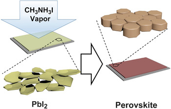
The key steps include the deposition of the inorganic framework by a solution process and subsequently, the in situ reaction between the inorganic species and the desired organic vapor, as shown in Figure 1 . Reference Chen, Zhou, Hong, Luo, Duan, Wang, Liu, Li and Yang13 It is critical to choose a source temperature that generates sufficient vapor pressure without damaging or decomposing the gaseous methylammonium salts completely. The substrate temperature will also influence the dynamics of perovskite formation. Under these conditions, a two-zone furnace has also been used to perform VASP, which allows for the fine-tuning of both the substrate and vapor source temperature. In addition, by changing the atmosphere of the furnace, undesirable side reactions can be excluded, and a pure perovskite film can be formed.
Schematic illustration of the proposed two-step vapor treatment for the fabrication of dense, continuous perovskite thin films. Adapted with permission from Reference 13. © 2014 American Chemical Society.

This method is conceptually different from either the solution process or vacuum deposition by avoiding the codeposition of organic and inorganic species. Incorporation of organic species through vapor effectively avoids the high growth rate of the perovskite component during co-deposition of precursors and the possible film deterioration upon dipping an inorganic framework into an organic solution. It utilizes the kinetic reactivity of the organic vapor and thermodynamic stability of perovskite during the in situ growth process. The perovskite films derived from this approach exhibit full surface coverage, uniform grain structures with grain sizes up to the micron scale, and complete precursor transformation. VASP offers wide flexibility for delicate control of film growth with retarded nucleation and vigorous re-organizational growth, and has evolved to solid-gas reaction processes and chemical vapor deposition (CVD) fabrication. Reference Leyden, Ono, Raga, Kato, Wang and Qi29,Reference Luo, Liu, Xia, Yuan, Cheng and Lu32–Reference Zhu, Yu, Li, Bao, Gao, Yi, Yang, Fu, Zhou and Zou34
Film quality
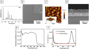
The perovskite film obtained from VASP has been characterized by combined structural, morphological, compositional, and optical measurements. Reference Chen, Zhou, Hong, Luo, Duan, Wang, Liu, Li and Yang13,Reference Luo, Liu, Xia, Yuan, Cheng and Lu32 Figure 2 a shows a typical x-ray diffraction spectrum of the as-prepared CH3NH3PbI3 film on fluorine-doped tin oxide/crystalline TiO2 (FTO/c-TiO2) substrate. A set of diffraction peaks at 14.08°, 28.41°, 31.85°, and 43.19°, assigned to (110), (220), (310), and (330), respectively, of the CH3NH3PbI3 crystal indicates a tetragonal crystal structure with high crystallinity. The absence of a diffraction peak at 12.65° in the perovskite film suggests complete consumption of PbI2 via VASP. Reference Chen, Zhou, Hong, Luo, Duan, Wang, Liu, Li and Yang13
Perovskite film on fluorine-doped tin oxide/crystalline TiO2 (FTO/c-TiO2) substrate, obtained via vapor-assisted solution process (VASP): (a) x-ray diffraction pattern; Reference Chen, Zhou, Hong, Luo, Duan, Wang, Liu, Li and Yang13 (b) top-view scanning electron microscopy (SEM) image (inset: image with higher resolution, scale bar = 1 μm); Reference Chen, Zhou, Hong, Luo, Duan, Wang, Liu, Li and Yang13 (c) tapping-mode atomic force microscopy height images (5 μm × 5 μm) (inset: corresponding 3D topographic image); Reference Chen, Zhou, Hong, Luo, Duan, Wang, Liu, Li and Yang13 and (d) cross-sectional SEM image. Reference Chen, Zhou, Hong, Luo, Duan, Wang, Liu, Li and Yang13 Perovskite film optical properties via chemical vapor deposition (CVD), and optical properties of CH3NH3PbI3 films obtained by CVD. (e) Absorption coefficient, Reference Luo, Liu, Xia, Yuan, Cheng and Lu32 which shows the perovskite exhibiting excellent light harvesting across the entire visible region; and (f) photoluminescence (PL), indicating the TiO2 effectively quenches the PL of the perovskite film. Reference Luo, Liu, Xia, Yuan, Cheng and Lu32 Adapted with permission from References 13 and 32. © 2014, 2015 American Chemical Society.

The scanning electron microscopy (SEM) image (Figure 2b) indicates that the as-formed perovskite film shows full surface coverage on the substrate with remarkable grain size up to the micron scale. Although, surprisingly, grain boundaries in this material system have been found to be electronically inert, the presence of large grain sizes is expected to promote improved charge extraction efficiency. By adjusting processing conditions, the grain size of the perovskite crystals is tunable from 200–300 nm to 1–2 µm, while still maintaining a continuous film. The surface roughness of the CH3NH3PbI3 film was generally measured to be approximately 20 nm (root-mean-square value) in an area range of 5 μm × 5 μm, through atomic force microscopy measurements (Figure 2c). Reference Chen, Zhou, Hong, Luo, Duan, Wang, Liu, Li and Yang13
A typical cross-sectional SEM image shows the perovskite film has a thickness of ∼350 nm, with well-defined grains across the film thickness (Figure 2d). Energy dispersive spectroscopy results indicate that the Pb/I ratio is very close to the desired stoichiometry (1:3) of CH3NH3PbI3 absorbers. Reference Luo, Liu, Xia, Yuan, Cheng and Lu32 The film presents broad strong absorption covering the entire visible range, and has an average value of ∼105 cm−1 (Figure 2e), resulting from the compact and highly uniform film quality.
The bandgap (E g) of the film was estimated to be ∼1.6 eV for both CH3NH3PbI3 and CH3NH3PbI3–x Cl x films. Reference Luo, Liu, Xia, Yuan, Cheng and Lu32 The photoluminescence spectrum of CH3NH3PbI3 films is right at the band edge with little Stokes shift (the difference in wavelength between the band maxima positions of the absorption and emission spectra) and shows a strong peak of ∼770 nm (Figure 2f), which implies that the photo-induced carriers accumulate at the band edge and produce light through direct recombination. Reference Luo, Liu, Xia, Yuan, Cheng and Lu32 Therefore, the 100% surface coverage, microscale grain size, uniform grain structure, and excellent carrier behavior of the as-prepared film suggest its promising applicability for PV devices. These overwhelmingly desirable characteristics could be due to the combination of the relative smoothness of the preformed PbI2 film and the effective intercalation of CH3NH3I vapor into the inorganic framework.
Film evolution
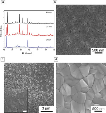
A thin-film evolution study indicated re-arrangement of the PbX2 film during CH3NH3I intercalation driven by a reduction in grain boundary energy. A typical example is the formation of CH3NH3PbI3, which has been reported in several studies. Reference Luo, Liu, Xia, Yuan, Cheng and Lu32,Reference Hao, Stoumpos, Liu, Chang and Kanatzidis35 Regardless of the reaction temperature, atmosphere, and pressure, the film evolution starts from PbI2, followed by an intermediate stage with a mixture of PbI2 and CH3NH3PbI3, and a final stage with complete formation of CH3NH3PbI3, as shown in Figure 3 . Reference Chen, Zhou, Hong, Luo, Duan, Wang, Liu, Li and Yang13,Reference Luo, Liu, Xia, Yuan, Cheng and Lu32,Reference Hao, Stoumpos, Liu, Chang and Kanatzidis35 Generally, the initial PbI2 film exhibits uniform polygonal grains of a few hundred nanometers in size, as well as scattered voids among adjacent grains. As the PbI2 film is exposed to CH3NH3I vapor, CH3NH3PbI3 gradually forms on the top of the original PbI2 film with larger grain size and different grain morphology.
Time evolution characterization of the perovskite thin film by annealing an ∼200-nm PbI2 film in the presence of CH3NH3I at 150°C in an N2 atmosphere: Reference Chen, Zhou, Hong, Luo, Duan, Wang, Liu, Li and Yang13 (a) x-ray diffraction patterns of the film annealed at 0, 0.5, and 4 h, where the phase converted from PbI2 to CH3NH3PbI3. Top-view scanning electron microscopy images of (b) the PbI2 film at the initial stage at 0 h, (c) the PbI2/CH3NH3PbI3 film at the intermediate stage at 0.5 h (inset: wider view, scale bar = 3 μm), and (d) the CH3NH3PbI3 film at the post-stage at 4 h. Adapted with permission from Reference 13. © 2014 American Chemical Society.

The newly formed CH3NH3PbI3 with crystal size ranging from tens of nanometers to micrometers become nucleation centers for subsequent film growth. Further intercalation reactions between PbI2 and CH3NH3I lead to complete conversion of PbI2 to perovskite films. During the process, film thickening occurs, as evidenced from the original PbI2 film of ∼200 nm thickness to a perovskite film of ∼350 nm thickness. This is likely due to volume expansion from intercalation of CH3NH3I, accompanied by transformation of the PbI2 framework from the original edge-sharing octahedral structures to the corner-sharing octahedral structures in perovskite films. The in-plane grain size of perovskite is three times the film thickness, indicating that the growth of perovskite polycrystalline films follows the normal grain growth mode. During crystallization of the perovskite film, a grain coarsening process is observed through the motion of grain boundaries, resulting in the shrinkage and elimination of small grains, which, in turn, results in an increase in the average size of the remaining grains. Such grain coarsening is mainly driven by the reduction in the total grain-boundary area and in the corresponding total grain-boundary energy that accompanies the area decrease.
In addition, the voids present in-between the adjacent crystals in the original PbI2 film vanishes after the perovskite crystals form. Interestingly, further prolonging the reaction time after the completed stage does not affect the grain structure, suggesting the absence of obvious ripening or coarsening processes. This further indicates that with a continuous supply of organic vapor, a thermodynamically stable film was maintained after the reaction had completed at a moderate temperature. This might also suggest that thermostability of perovskite films is achievable under certain circumstances, where the solid-gas reaction pathway could benefit the long-term device thermostability.
Comparison with conventional solution process
The VASP process described here yields high-quality perovskite films, while the film growth characteristics and underlying mechanisms differ from those of other conventional solution processes. In terms of nucleation and film growth, the two-step VASP exhibits a retarded nucleation and enhanced re-organization growth. The prevention of nucleation is achieved by the separate deposition of the inorganic and organic counterparts in the VASP approach. The preformed PbI2 film acts not only as a superior framework for perovskite formation, but also as a reservoir for one of the reactants to provide kinetically favorable “nucleation” centers for further perovskite formation.
During the transformation from PbI2 to perovskite by the intercalation of CH3NH3I, vigorous rearrangement of the aggregate PbI2 structure or the newly formed CH3NH3PbI3 occurs, driven by a reduction in grain-boundary length to minimize the grain-boundary energy. Thus, smooth, pinhole-free perovskite films with uniform grain structures are obtained. In contrast, conventional solution processes based on co-deposition of organic and inorganic counterparts with appropriate stoichiometry initiates fast nucleation, followed by a grain growth process due to the extremely high reaction rate of the perovskite film. Control over nucleation and growth in a conventional solution process is heavily dependent on other strict kinetic parameters (e.g., solvent engineering enables a window for fast deposition–precipitation out of the solution to form a smooth perovskite film). Reference Jeon, Noh, Kim, Yang, Ryu and Seok22
VASP also shows superior capability for the processing of a variety of hybrid materials, regardless of dimensionality. Although a two-step dipping process based on dipping the pre-formed inorganic framework into an organic solution can effectively separate the film nucleation and grain growth processes, the extension of this method for the formation of three-dimensional hybrid perovskite materials is limited. VASP is more applicable for fabricating 3D structured perovskite thin films, which are particularly suitable for PV operation, compared to the conventional two-step dipping process. As there is no kinetically favorable van der Waals gap in the interface where the transformation occurs for 3D perovskite, a rather long reaction time is required to completely transform inorganic precursors into a final product. Additionally, films often deteriorate upon extended dipping, due to the existence of solvent media. In VASP, the absence of solvent media and moderate processing temperature collectively enable a complete reaction between PbX2 and CH3NH3X without impairing the film quality while obtaining respectable small surface roughness. Reference Chen, Zhou, Hong, Luo, Duan, Wang, Liu, Li and Yang13
Aside from the previous, films derived from VASP may potentially exhibit higher stability due to the absence of the formation of intermediate complexes consisting of precursors and solvents. It has been shown that in the commonly applied solution process, the solvents (e.g., dimethylsulfoxide [DMSO], N,N-dimethylformamide [DMF], or small amounts of H2O) can interact with the precursors or perovskite and form stable solvates, such as CH3NH3PbI3·DMSO, CH3NH3PbI3·DMF and CH3NH3PbI3·H2O. Reference Jeon, Noh, Kim, Yang, Ryu and Seok22,Reference Hao, Stoumpos, Liu, Chang and Kanatzidis35,Reference You, Yang, Hong, Song, Meng, Liu, Jiang, Zhou, Chang, Li and Yang36 Common features of the intermediate phases are always in the form of a needle-shaped morphology, distinctively characterized by low-angle x-ray diffraction reflections (typically 2θ < 10°, where θ is the angle of incidence), without a confirmed crystal structure. The tendency of CH3NH3PbI3 to incorporate a neutral small molecule while accompanied by a profound change in its crystal structure is universal.
In the perovskite structure, [PbI3]− fragments adopt “double-chain” assembly, characterized by three fused [PbI6]4− octahedra sharing a common corner, and the inserted CH3NH3 + cations stabilize the negatively charged [PbI3]− chains through electrostatic interactions. Reference Hao, Stoumpos, Liu, Chang and Kanatzidis35 The guest DMF, DMSO, or H2O molecules provide extra stability to the crystal structure by means of a strong asymmetric or symmetrical H-bonds. These intermediate phases are more reactive than PbI2 itself and are thus expected to facilitate subsequent crystallization processes of the corresponding perovskite film. However, the solvation and hydration processing and undesirable structural transitions greatly increase the complexity of the perovskite system, suggesting decreased controllability for film formation. VASP provides a practical solution to address the previous challenge.
Therefore, the structural correlations in ABX3 highlight why the VASP method is very appealing and provide a consistent approach for the fabrication of robust perovskite layers in solid-state solar cells. More importantly, the absence of possible solvation and hydration processing and undesirable structural transitions will further benefit film stability, resulting in long-term stability of the devices. A recent publication has suggested apparent evidence of a film, prepared by the analogous low pressure CVD method, showing much slower decomposition in ambient air, thus indicating better moisture resistance. Reference Luo, Liu, Xia, Yuan, Cheng and Lu32
Perovskite device performance based on vapor-assisted solution process
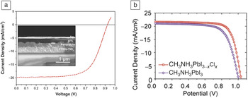
Device performance of perovskite solar cells based on VASP has steadily improved. The first attempt at VASP CH3NH3PbI3 enabled a PCE of 12.1% in a planar architecture, with current density–voltage (J–V) characteristics shown in Figure 4 a, which at that time was one of the highest efficiencies achieved by a CH3NH3PbI3 planar heterojunction configuration. Reference Chen, Zhou, Hong, Luo, Duan, Wang, Liu, Li and Yang13 Later efforts, through simple switching of the precursors, such as changing the mixture of PbI2 to PbCl2, under low-pressure deposition further demonstrated an efficiency of 16.8%; the J–V curve is shown in Figure 4b. Reference Li, Cooper, Buonsanti, Giannini, Liu, Toma and Sharp37
The characteristics of solar-cell performance: (a) current density−voltage (J−V) characteristics of the solar cell based on the vapor-assisted solution process (VASP) method under air mass 1.5G illumination, and (inset) cross-sectional scanning electron microscopy image of the device; Reference Chen, Zhou, Hong, Luo, Duan, Wang, Liu, Li and Yang13 the device performance (power-conversion efficiency) is 12.1%. (b) J−V curves of CH3NH3PbI3 (blue curve) and CH3NH3PbI3−x Cl x (red curve)-based solar cells, derived from low-pressure VASP Reference Li, Cooper, Buonsanti, Giannini, Liu, Toma and Sharp37 with a device performance of 16.8%. Note: HTL, hole-transporting layer; FTO, fluorine-doped tin oxide; c-TiO2, crystalline TiO2. Adapted with permission from References 13 and 37. © 2014, 2015 American Chemical Society.

One of the most important advantages of VASP-based perovskite solar cells is the high reproducibility of high-quality films and PCE devices. A PCE of over 10.6% has been realized with negligible standard deviation, where the perovskite film was fabricated by the presented solid-gas reaction, and the device architecture was free of a hole transport material. Reference Hao, Stoumpos, Liu, Chang and Kanatzidis35 All other devices derived from the analogous processing method (e.g., CVD) present respective efficiencies of over 10%. Reference Leyden, Ono, Raga, Kato, Wang and Qi29,Reference Luo, Liu, Xia, Yuan, Cheng and Lu32
Devices based on VASP have excellent short-circuit current densities and show no sign of shunt pathways through the absorber film. Additionally, the improved grain sizes of the perovskite films help reduce the presence of grain-boundary traps and relax the severity of charge-carrier scattering, leading to decreased recombination and enhanced absorber performance. As an additional benefit, the tunable grain size of the perovskite films could offer an excellent opportunity to study the relationship between grain boundaries and device performance in this system.
Summary and outlook
VASP is one of the most successful methods for the formation of organic–inorganic perovskite films, since the first report of perovskite nanoparticles coated on a mesoporous TiO2 electrode in a dye-sensitized solar-cell structure. Although the performance of devices fabricated by VASP has been surpassed by devices fabricated by recent optimizations and alternative methods, this method is a highly competitive one for mass production in a reproducible and cost-effective manner. It also provides essential characteristics, such as complete surface coverage to prevent low-resistance shunting paths between the n- and p-type contacts, and for high-performance planar heterojunction solar cells.
Previously, there have been a myriad of approaches, including one-step vacuum and solution co-deposition and two-step methods that involve a solvent and vapor, or post-treatments, which deliver perovskite films with compact and large crystalline domains. Different from these various methods that achieve high-quality grains, VASP is based on the introduction of fast crystallization through retarding nucleation and reorganizing film growth. The resulting films have demonstrated high-quality and high-performance PV devices with PCE values of ∼17%, which could be considered an additional advantage to the VASP characteristics of simplicity, controllability, and versatility.
It is still unclear why the efficiency of perovskite solar cells based on VASP, regardless of its quality, is slightly lower than that of devices derived from an optimized solution process (certified over 20%). Our interpretation of the present device performance is based on the possibly of existing defects or traps, as the reaction is carried out in the range of 120°C to 150°C, where the gaseous CH3NH3X decomposes into HX and CH3NH2. According to theoretical calculations, the presence of iodine interstitials within the perovskite crystal structure has a relatively deeper energy level, which probably serves as a recombination center for photogenerated carriers. We suspect that certain amounts of defects or traps could be present in the perovskite film obtained from the VASP method, and capacitance–voltage measurements have yielded an energy level of 0.156 eV (considered as a deep-defect level) in the perovskite film. The presence of defects or traps in the perovskite film is not unique to the VASP method. Proper passivation of the polycrystalline perovskite film might lead to generally superior properties compared to its current counterparts.
Continuous progress on film formation will lead to improved perovskite solar cells and other organic–inorganic hybrid optoelectronics. Future studies on the VASP technique should focus on understanding the origins of defect states and exploration of surface and grain-boundary passivation. We anticipate that with continued progress of film formation, perovskite solar cells could be a highly competitive technology in the PV field, with anticipated PCE values approaching 25% within the next few years.
Acknowledgment
The authors sincerely thank Nicholas De Marco for his assistance in editing.