I. INTRODUCTION
The III-nitrides including the semiconductors AlN, GaN, and InN form a continuous AlGaInN alloy system with direct band gaps, ranging from about 0.7 eV (InN) to 6.2 eV (AlN) with 3.4 eV for GaN. Band gaps from 0.7 to 6.2 eV could be obtained by suitable alloy combinations in the AlGaInN system to tailor the band gap energy of the active region spanning the entire UV and visible ranges.Reference Kuen, Fong, Chan and Surya1–Reference Wang, Liu, Yang, Lin, Zhou, Qian and Li4 Therefore, the III-nitride semiconductors have attracted considerable attention as promising materials for the application of light-emitting diodes (LEDs), especially, in general lighting and liquid crystal display backlighting, and most of outdoor commercial displays.Reference Jia, Yu, Lu, Zhong, Sun, Tong and Zhang5,Reference Zhang, Shao, Hao, Wu, Zhang, Qu, Chen and Xu6 As the rapid improvement of nitride semiconductor epitaxial growth technology, the internal quantum efficiency (IQE) for red and blue LEDs has achieved above 50 and 60%, respectively.Reference Lin, Lee, Liu, Han, Lan, Lin, Chi and Kuo7,Reference Lee, Limb, Ryou, Yoo, Ewin, Korenblit and Dupuis8 However, as for the green LEDs, it is just about 30%. So far, tremendous works have been pursued to address the efficiency issue in InGaN-based LEDs.Reference Crawford9,Reference Tansu, Zhao, Liu, Li, Zhang, Tong and Ee10 The existence of electrostatic fields in InGaN quantum well (QW) results in charge separation issue.Reference Brown, Blood, Smowton, Thomson, Olaizola, Fox, Parbrook and Chow11,Reference Zhao, Arif, Ee and Tansu12 For the InGaN/GaN green LEDs, high indium composition is required for the growth of InGaN/GaN multiple quantum wells (MQWs), which results in the high piezoelectric field in MQWs.Reference Feezell, Speck, DenBaars and Nakamura13–Reference Zhao, Liu, Li, Huang, Poplawsky, Penn, Dierolf and Tansu17 This leads to the formation of quantum confined Stark effects (QCSEs) and subsequently causes the separation of electrons and holes, thus, decreasing the IQE of InGaN/GaN green LEDs ultimately.Reference Feezell, Speck, DenBaars and Nakamura13–Reference Zhao, Liu, Li, Huang, Poplawsky, Penn, Dierolf and Tansu17 Recent work has also identified the importance of Auger process in InGaN-based LEDs,Reference Iveland, Martinelli, Peretti, Speck and Weisbuch18,Reference Tan, Zhang, Li, Liu, Tayo and Tansu19 and the use of a new type material is expected to suppress this issue.Reference Tan, Zhang, Li, Liu, Tayo and Tansu19–Reference Zhao, Arif and Tansu21 Nevertheless, technical challenges still exist in achieving high-quality InGaN/GaN MQWs due to the large lattice and thermal expansion coefficient mismatches between GaN and InGaN alloys.Reference Kuen, Fong, Chan and Surya1,Reference Gao, Guan, Li, Gao, Guo and Li2 Additionally, the growth of p-GaN needs higher growth temperature compared with the InGaN/GaN MQW active layer growth, which may cause serious fluctuation of indium composition, and eventually lead to the degradation of the structural and optical properties of green MQWs. In this regard, enormous attention has been paid to the fabrication of high quality InGaN/GaN green MQWs.Reference Lee, Chen and Lee22,Reference Yang, Cao and Yan23 Most of the InGaN/GaN green LEDs' researchers concentrate on the optimization of the MQW growth parameters for achieving high quality MQWs to achieve highly efficient InGaN/GaN green LEDs.Reference Chang, Lai, Su, Chen, Liu and Lia24,Reference Ryou, Limb, Lee, Liu, Lochner, Yoo and Dupuis25 Meanwhile, the subsequent heat treatment is also a tremendously important part for the growth of p-GaN, as well as the restrict control for the epitaxial growth of high quality MQWs. There are many reports about decreasing the epitaxial growth temperature of p-GaN to achieve highly efficient InGaN/GaN green LEDs, but few works focus on the systematic study of the p-GaN growth temperature effects on the green MQWs and its growth mechanism.Reference Daele, Tendeloo, Jacobs, Moerman and Leys26,Reference Limb, Lee, Ryou, Yoo and Dupis27
In this work, we report on the systematic study of the influence of p-GaN layer growth and its growth temperature on the structural and optoelectronic properties of InGaN/GaN green LEDs. The as-grown MQWs and InGaN/GaN green LEDs are characterized by high-resolution x-ray diffraction (HRXRD), photoluminescence (PL), electroluminescence (EL), voltage (V)–current (I) curve, and light output power (L)–I curves for structural and optoelectronic properties. This work obtains the optimized epitaxial growth parameters of p-GaN layer for realizing the highly efficient InGaN/GaN green LED devices.
II. EXPERIMENTAL
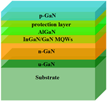
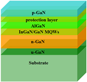
All the samples of InGaN/GaN MQWs and InGaN/GaN green LED wafers were grown on sapphire (0001) substrates by a vertical Veeco metal-organic chemical vapor deposition (MOCVD) system. During the growth, trimethylgallium (TMGa), trimethylindium (TMIn), triethylaluminum (TMAl), and ammonia (NH3) were used as the precursors for Ga, In, Al, and N, respectively. Biscyclopentadienyl magnesium (CP2Mg) and silane (SiH4) were used as the p-type and n-type doping sources, respectively. Nitrogen (N2) was the carrier gas for the epitaxial growth of MQW structures, while hydrogen (H2) was for the other structures. The schematic diagram of the InGaN/GaN green LED structure is shown in Fig. 1. Three samples were prepared with different structures and epitaxial growth parameters. The InGaN/GaN green LEDs were prepared as follows: 4 μm-thick unintentional doped GaN films were firstly grown, and then 3 μm-thick Si-doped n-GaN films were grown. Subsequently, 6-period In0.2Ga0.8N (2 nm)/GaN (16 nm) MQWs were grown by modulated temperature growth mode, that is, the growth temperatures for the GaN barrier and InGaN well layers are different. In our case, the growth temperatures for barrier and well layers were 850 and 750 °C, respectively. Afterward, a 2 nm-thick pure GaN covering layer was grown after MQWs' epitaxial growth with the temperature of 850 °C to avoid the volatilization of indium composition, followed by the growth of a 20 nm-thick Mg-doped p-AlGaN layer. Finally, 150 nm-thick Mg-doped p-GaN films were grown at the growth temperature of 920, 950, and 980 °C for Sample A, Sample B, and Sample C, respectively. After the epitaxial growth, the samples were annealed in an annealing furnace (America, Allwin21 Corp. AccuThermo AW810M) for 60 min at the optimized temperature of 950 °C to remove the H-complex bonding in the alloy. To investigate the properties of InGaN/GaN MQWs and their influence by the p-GaN layer growth, several MQWs were grown without the growth of p-GaN. After the epitaxial growth, all the samples were characterized by HRXRD (Bruker D8 x-ray diffractometer with Cu Kα1 x-ray source λ = 1.5406 Å) for crystalline quality and PL measurement by using a 405 nm laser (YWafer GS4-GaN-R-405) with an output power of 20 mW for optical properties. The as-grown LED wafers were fabricated into LED chips by the standard procedure.Reference Wang, Yang and Li28,Reference Wang, Lin, Yang, Liu, Zhou, Qian, Gao, Wen and Li29 The optoelectronic properties of chips were studied by CMC-2004 and Ocean Optics USB 2000 spectrometry, respectively.
The schematic diagram of InGaN/GaN green LED structure.
III. RESULTS AND DISCUSSION
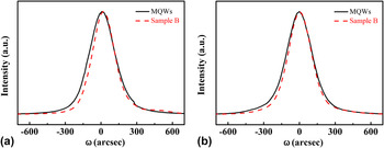
In this section, the structural and optical properties of as-grown MQWs without epitaxial growth of p-GaN layer and Sample B with a full LED structure are carefully studied. The x-ray rocking curves for GaN (0002) and (10−12) planes of MQWs and Sample B are shown in Figs. 2(a) and 2(b), respectively. The full width at half maximum (FWHM) values of the GaN (0002) plane for the MQWs and Sample B are 252 and 231 arcsec, respectively. Meanwhile, the FWHM values of the GaN (10−12) plane for the MQWs and Sample B are 265 and 247 arcsec, respectively. It is known to us that the FWHM value for the GaN (0002) plane is related to the densities of screw dislocation in GaN films, which mainly generated from the different step heights of the substrates. While the FWHM value for GaN (10−12) is related to the densities of the mixed and pure edge dislocations that generated from the coalescence process among the misoriented individual islands.Reference Li, Jiang, Fana, Fang and Wang30,Reference Liu, Tsai, Yen, Chen, Tsai, Huang, Chen, Hsu and Liu31 The densities of dislocations in MQWs and Sample B can be approximately evaluated as:Reference Liu, Tsai, Yen, Chen, Tsai, Huang, Chen, Hsu and Liu31
 $${D_{{\rm{dis}}}} = {{{\beta ^2}} \over {9{b^2}}}\quad {\rm{,}}$$
where D dis is the density of dislocation, β is the FWHM value, and b is the length of the Burger vector of the corresponding dislocations. The FWHM values of (0002) and (10−12) for both InGaN/GaN green LEDs and MQWs are listed in Table I. Based on Eq. (1) and Table I, the densities of screw, pure edge, and mixed dislocations in n-GaN after the growth of the p-GaN layer are decreased with the values of 16 and 13%, respectively, when compared with those of the MQWs without growth of p-GaN layer. Meanwhile, as the increase in p-GaN layer growth temperature, the crystalline quality of n-GaN films gradually increases, as shown in Table I. We ascribe it to the high growth temperature of p-GaN that enhances the migration distance of Ga atoms incorporating into the lattice of the defect locations, suppresses the edge and screw dislocations, and therefore improves the GaN crystalline quality ultimately. The higher the p-GaN growth temperature is, the better the n-GaN crystalline quality will be. Meanwhile, the crystalline quality of these InGaN/GaN green LEDs is comparable with that of the state-of-the-art InGaN/GaN blue LEDs grown on sapphire and patterned sapphire substrates.Reference Wang, Zhou, Lin, Hong and Li32
The comparison of (a) (0002) and (b) (10−12) rocking curves for MQWs and Sample B.

The FWHM values of PL, EL, and XRD for MQWs, Samples A, B, and C.

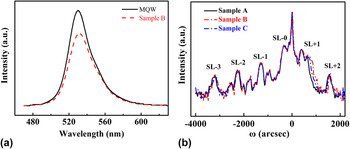
Figure 3(a) shows the comparison of PL spectrum for both the MQW structure without growth of p-GaN layer and Sample B. The FWHM value of the PL peak for MQW structure is 29 nm, while for Sample B is 33 nm (Table I), which is attributed to the stacked growth of p-GaN layer on the MQWs that increases the light emitting energy level, leading to the broadening in PL peaks ultimately.Reference Lin, Ma, Hsu, Feng, Cheng, Liao, Yang, Chou, Lee and Chyi33 This is quite different from the blue MQWs and blue LEDs, and the peak of PL spectrum for blue LEDs is just a little broadening due to the lower indium composition in the InGaN well layer.Reference Lin, Ma, Hsu, Feng, Cheng, Liao, Yang, Chou, Lee and Chyi33 It is believed that the p-GaN epitaxial growth makes a negative effect on the green MQW structure in green LEDs, where high indium composition in InGaN wells is existed. The p-GaN layer growth would exacerbate indium composition fluctuation to a certain extent and deteriorate the crystalline qualities and optical properties of the MQWs ultimately.Reference Dupuis, Limb, Liu, Ryou, Horne and Yoo34,Reference Lv, Wang, Wang, Hao and Luo35 However, the comparison test of the blue LEDs shows a contrary result, because the exacerbated fluctuation indium in the blue MQWs is beneficial to the carrier confinement that enhances the radiation recombination efficiency to some extent.Reference Dupuis, Limb, Liu, Ryou, Horne and Yoo34,Reference Lv, Wang, Wang, Hao and Luo35
(a) The PL spectrum for MQWs and Sample B and (b) the comparison of ω–2θ rocking curves for Sample A, Sample B, and Sample C.

It is not hard to find that the p-GaN epitaxial growth temperature makes a tremendous effect on the status of MQWs in LED wafers. In this work, the crystalline qualities of InGaN/GaN MQWs influenced by the growth temperature of p-GaN layer are studied by ω–2θ rocking curves, as shown in Fig. 3(b). On the one hand, if the epitaxial growth temperature for p-GaN is as low as 920 °C, one can note the broadened satellite peaks in typical ω–2θ rocking curves of Sample A when compared with that of Sample B grown at 950 °C. On the other hand, if the p-GaN epitaxial growth temperature is increased to 980 °C, one can also clearly identify the broadened in satellite peaks for MQWs in Sample B as compared with that of Sample C. Furthermore, the FWHM values of satellite (SL)-3 peaks are 260, 220, and 272 arcsec for Sample A, Sample B, and Sample C, respectively, which indicates the poorer crystalline quality of the MQWs in Sample A and Sample C when compared with that of Sample B. We attribute these results to the following reason. If the growth temperature of p-GaN layer is too low, it may not supply enough energy to enhance the crystalline quality of InGaN/GaN MQWs even though the fluctuation of indium composition in InGaN wells is suppressed. On the contrary, if the growth temperature of p-GaN layer is too high, the fluctuation of indium composition in InGaN wells will happen, and the crystalline quality of InGaN/GaN MQWs is significantly reduced. The optical properties of InGaN/GaN MQWs influenced by the growth temperature of p-GaN layer are also studied. If the p-GaN epitaxial growth temperature is decreased to 920 °C, as shown in Sample A, it also shows poorer optical properties of as-grown InGaN/GaN green LEDs with a broadened PL peak. This may be ascribed to the poorer Mg doping rate at lower growth temperature, which leads to the poorer quality of as-grown p-GaN and eventually results in the decline of effective recombination efficiency. Meanwhile, the broadened emission peaks of PL spectra for Sample C prove that the increase of the p-GaN growth temperature would further exacerbate the fluctuation of indium composition in the original high stressed green QW (Table I).
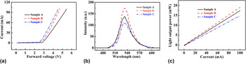
We further study on the optoelectronic properties of the InGaN/GaN green LED devices that affected by the p-GaN epitaxial growth temperature. Figure 4(a) shows the comparison of V–I curves for LEDs of Sample A, Sample B, and Sample C, respectively. At an injection current of 20 mA, the forward voltages are of 3.43, 3.21, and 3.01 V for these three samples, respectively. One can clearly find that the increase of the p-GaN epitaxial growth temperature obviously benefits to the improvement of electronic properties of InGaN/GaN green LEDs. On the one hand, when the growth temperature of p-GaN layer is increased, the N vacancies and H atoms together with other impurities incorporated into p-GaN are dramatically reduced, while the activation rate of Mg atoms is also greatly improved.Reference Ju, Zhu, Kim, Lee and Lee36,Reference Taniyasu, Carlin, Castiglia, Butté and Grandjean37 On the other hand, the series resistance rate of device is decreased significantly and the conductivity of layer rather than InGaN/GaN MQWs may be improved to some extent with the increase in the growth temperature.Reference Ju, Zhu, Kim, Lee and Lee36,Reference Taniyasu, Carlin, Castiglia, Butté and Grandjean37 As a result, these lead to the decrease of forward voltage. Although the higher p-GaN epitaxial growth temperature improves the electrical properties of InGaN/GaN green LED devices, it damages the MQW structure because the FWHM of EL peak for Sample C LEDs increases 5 nm compared with that of Sample B LEDs, and the emission intensity decreases to 69% for Sample C LEDs when compared with that of Sample B LEDs [Fig. 4(b) and Table I]. Meanwhile, with the decrease in the p-GaN growth temperature, the worse Mg doping efficiency leads to the poorer light output power, which leads to the decline of emission peak intensity. In this case, the peak intensity for Sample A LEDs is just about 78% when compared to that for Sample B LEDs. These comparisons indicate that the growth temperature of p-GaN layer plays a great impact on the MQW structures. Although the enriched indium is beneficial to the carriers' confinement state and enhances the recombination, it is also very easy to induce V-defects that decrease the conductivity in the InGaN/GaN and the effective recombination of electrons and holes.Reference Yong, Soh, Zhang, Chow and Chua38–Reference Oh, Kwon, Park, Baek, Park, Lee and Jung42 The negative effects of excessive p-GaN epitaxial growth temperature on the MQWs can be seen from the changes in the reverse current (reverse voltage is –7 V), the reverse current value of Sample C is 48 μA, while the reverse current for the Sample B LEDs is only 0.01 μA. This increase of reverse current is related to the MQW structure, which releases the stress by the formation of the more defects under the higher p-GaN epitaxial growth temperature. Figure 4(c) shows the light output power for LEDs dependence on the forward current. As for Sample A LEDs and Sample B LEDs, the light output power of Sample B LEDs is higher than that of Sample A LEDs, since the lower growth temperature results in the poorer Mg doping rate, leads to the worse effective recombination, and therefore results in the decline of the light output power ultimately. In the Sample B LEDs and Sample C LEDs case, the light output power of Sample B LEDs is higher than that of Sample C LEDs, which is attributed to the too high growth temperature of p-GaN. This deteriorates the crystalline quality of MQWs, leading to the poor conductivity of InGaN/GaN MQWs and low effective recombination between holes and electrons, and eventually poor optoelectronic properties of LEDs. Based on these results, we therefore can make a conclusion that the p-GaN layer growth temperature of 950 °C is most suitable for obtaining highly efficient InGaN/GaN green LEDs.
(a) V–I, (b) EL, and (c) L–I curves for various LED devices.

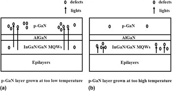
Based on the above discussion, the mechanisms for the effect of p-GaN growth temperature on the properties of InGaN/GaN green LEDs can be deduced. As for the p-GaN layer grown at low temperature, the Mg doping rate is very poor, and many defects may form during the p-GaN growth, as illustrated in Fig. 5(a). These defects may capture the carriers, increase the absorption of lights when they pass through the p-GaN layer, and eventually reduce the light extraction efficiency of InGaN/GaN green LEDs. In this case, the defects caused by the fluctuation of indium composition in InGaN wells are very few due to their low growth temperature. Therefore, the absorption of lights in InGaN/GaN MQW layers is very few. While for the p-GaN layer grown at too high temperature, the high-quality p-GaN layer can be grown due to the fact that the N vacancies and H atoms together with other impurities incorporated into the p-GaN layer are dramatically reduced, and the activation rate of Mg atoms is also greatly improved. Therefore, the formed defects by the Mg doping in the p-GaN layer are significantly reduced, and the lights absorbed by the p-GaN layer are greatly reduced. However, in this case, the serious fluctuation of indium composition in InGaN well would take place, and many defects are formed in InGaN/GaN MQWs, as shown in Fig. 5(b). This process also increases the absorption of lights and reduces the light extraction efficiency of InGaN/GaN green LEDs. Conclusively, the growth temperature of the p-GaN layer plays an important role in achieving highly efficient InGaN/GaN green LEDs.
Schematic diagram for p-GaN grown at too (a) low temperature and (b) high temperature.

IV. CONCLUSIONS
To summarize, this work systematically discusses the p-GaN growth and its growth temperature influence on the structural and optoelectronic properties of InGaN/GaN green LEDs. It could be found that as the growth of the p-GaN layer, the crystalline quality of as-grown n-GaN improves significantly. Meanwhile, as the increase in the epitaxial growth temperature of p-GaN layer, the crystalline quality of n-GaN gradually improves. This may be ascribed to the high growth temperature that enhances the migration distance of Ga atoms incorporating into the lattice of the defect locations, suppresses the edge and screw dislocations subsequently, and improves the GaN crystalline quality ultimately. However, on the one hand, the LED with lower epitaxial growth temperature of the p-GaN layer shows the poorer optoelectronic properties, due to its poorer Mg doping rate, which leads to the poorer quality of as-grown p-GaN and eventually results in the decline of effective recombination efficiency. On the other hand, the excessively high epitaxial growth temperature of p-GaN layer deteriorates the structural and optoelectronic properties of MQWs in LEDs. The excessively high epitaxial growth temperature exacerbates the fluctuations of indium in the MQW structure, which leads to the formation of many nonradiative recombination centers, broadens the PL peak, reduces the light emission intensity, and eventually deteriorates the performance of green LED devices. Therefore, the optimized epitaxial growth temperature of the p-GaN layer is of significant importance in achieving highly efficient InGaN/GaN green LEDs. This work provides an improvement direction for optimizing the highly efficient InGaN/GaN green LEDs.
ACKNOWLEDGMENTS
This work is supported by National Science Fund for Excellent Young Scholars of China (No. 51422203), National Natural Science Foundation of China (No. 51372001), Excellent Youth Foundation of Guangdong Scientific Committee (No. S2013050013882), Key Project in Science and Technology of Guangdong Province (No. 2011A080801018), Strategic Special Funds for LEDs of Guangdong Province (Nos. 2011A081301010, 2011A081301012, and 2012A080302002), and Key Project in Science and Technology Innovation of Guangdong Province (No. cxzd1105).