I. INTRODUCTION
Ferroelectric films have received much attention for various applications, including nonvolatile ferroelectric random access memoriesReference Auciello, Scott and Ramesh 1 and sensors and actuators in microelectromechanical systems.Reference Muralt 2 , Reference Trolier-McKinstry and Muralt 3 Lead titanate (PbTiO3) is not only one of the most fundamental ferroelectric material with a high ferroelectricityReference Vrejoiu, Rhun, Pintilie, Hesse, Alexe and Gosele 4 but also the end member of the important ferroelectric and piezoelectric material systems, such as PbTiO3–PbZrO3 [Pb(Zr,Ti)O3], PbTiO3–Pb(Mg1/3Nb2/3)O3, etc.Reference Dawber, Lichtensteiger, Cantoni, Veithen, Ghosez, Johnston, Rabe and Triscone 5 Therefore, PbTiO3 films have been widely investigated in both polycrystalline formReference Li, Wu, Ge, Wang, Wang, Wang, Liu and Ming 6 and as epitaxially grown films as well.Reference Wasa, Haneda, Sato, Adachi, Kanno, Schlom, Trolier-Mckinstry, Gan and Eom 7 – Reference Fujisawa, Seioh, Kume and Shimizu 15 However, reported data of large ferroelectric properties for PbTiO3 films comparable to single crystal ferroelectricity are limited due to the measurement difficulty. The investigation of changes in ferroelectric properties on a wide range of film thickness has been hardly reported.
The difficulty of measuring ferroelectricity in PbTiO3 films has various origins. Many authors have pointed out the important role of misfit strain,Reference Martin 16 , Reference Ederer and Spaldin 17 thermal strain,Reference Fujisawa, Nakaki, Ikariyama, Morioka, Yamada, Saito and Funakubo 18 and film thicknessReference Lee, Nakhmanson, Chisholm, Christen, Rabe and Vanderbilt 19 as possible root causes of measurement difficulty. However, detailed mechanisms involving internal strain are not yet fully understood. For instance, some authors suggested that substrate-induced strain plays an important role in modifying structural and electrical properties of ferroelectric materials, as it influences the thermodynamic stability of ferroelectric phase.Reference Li, Hu, Liu and Chen 20 The interaction between internal strain and film thickness in PbTiO3 films can also be highlighted as a key factor, due to the possibility that it inhibits the growth and the coalescence of switched domains as has been reported on BaTiO3 films.Reference Jo, Kim, Noh, Yoon and Song 21
We reported previously on the crystal structure of epitaxial PbTiO3 films grown on calcium fluoride (CaF2) substrate, but polarization versus electric field (P–E) hysteresis loops have been hardly obtained.Reference Utsugi, Fujisawa, Ikariyama, Yasui, Nakaki, Yamada, Ishikawa, Matsushima, Morioka and Funakubo 22 , Reference Nakaki, Kim, Yokoyama, Ikariyama, Nishida, Saito and Funakubo 23
In the present study, (100)/(001)-oriented epitaxial PbTiO3 films are successfully grown on (100)cSrRuO3-covered (100)CaF2 substrates by metal organic chemical vapor deposition (MOCVD). Substrates made of CaF2 have a larger thermal expansion coefficient (18.9 × 10⁻⁶ K−1) than conventionally used substrates, such as those made of SrTiO3 (11.2 × 10⁻⁶ K−1) and MgO (13.5 × 10⁻⁶ K−1). This induces a larger compressive thermal strain applied to the films at the Curie temperature during cooling process after deposition, which is expected to lead to a larger volume fraction of (001) orientation, c-domain, than that measured on PbTiO3 films grown on SrTiO3 substrate.
In addition, CaF2 thermal expansion coefficient is similar to the a-axis of PbTiO3 films. Thus, in-plane a-axis lattice parameter change in (001)-oriented films is not strongly affected by thermal strain from the substrates during cooling process below the Curie temperature. This shows the possibility of growing epitaxial PbTiO3 films with larger volume fraction of (001)-oriented domain, V c, than the widely reported values for the films grown on SrTiO3 and MgO substrates. Hence, this large c-domain volume fraction is expected to be accompanied with a small residual strain, as previously obtained in our (001)-oriented Pb(Zr0.4Ti0.6)O3 epitaxial films grown on CaF2 substrates.Reference Fujisawa, Nakaki, Ikariyama, Yamada, Ishikawa, Morioka and Funakubo 24 As a consequence of this high c-domain volume fraction, a large remnant polarization is expected (>60 μC/cm2), close to the estimated spontaneous polarization of PbTiO3 single crystal for a wide range of film thickness from 60 to 2000 nm.
II. EXPERIMENTAL
Epitaxial (100)/(001)-oriented PbTiO3 films are grown at 600 °C on (100)cSrRuO3//(100)LaNiO3//(100)CaF2 and (100)SrRuO3//(100)SrTiO3 substrates by MOCVD from Pb(C11H19O2)2–Ti(O-i-C3H7)4–O2 system.Reference Utsugi, Fujisawa, Ikariyama, Yasui, Nakaki, Yamada, Ishikawa, Matsushima, Morioka and Funakubo 22 Radio frequency magnetron sputtering method is used to grow the 40–50-nm-thick SrRuO3 and LaNiO3 layers. SrRuO3 layer is used as the bottom electrode and LaNiO3 layer is used as a buffer layer to grow the conductive bottom layer on CaF2 substrate. Indeed, the large lattice mismatch between CaF2 and SrRuO3 requires an intermediate lattice parameter.
Crystal structure is investigated by high-resolution x-ray diffraction (XRD) using a four-axis diffractometer (PANalytical X’Pert MRD, Almelo, Netherlands). XRD is also used to estimate the volume fraction of (001)-oriented domains, V c = V(001)/[V(100) + V(001)], in the mixed orientation films of (001) domain (c-domain) and (100) domain (a-domain). Furthermore, residual strain in the films is measured by the Raman spectroscopy.
Ferroelectricity of SrRuO3/PbTiO3/Pt capacitor structure is measured using a ferroelectric tester (Toyo Corp. FCE-1, Tokyo, Japan) after preparing about 100-μm-diameter Pt top electrodes by electron beam evaporation.
III. RESULTS AND DISCUSSIONS
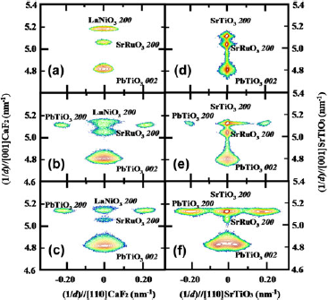
Figure 1 shows the XRD-reciprocal space mapping (XRD-RSM) near PbTiO3 200/002 of PbTiO3 films grown on CaF2 substrates [Figs. 1(a)–1(c)] and on SrTiO3 substrates [Figs. 1(d) and 1(e)] having a thickness ranging between 50 and 1300 nm. Horizontal and vertical axes in these figures correspond to the reciprocal of in-plane and out-of-plane lattice parameters, respectively. Only, PbTiO3 002 peaks are observed for very thin films samples (less than 60 nm) [Figs. 1(a) and 1(d)], suggesting a perfect (001) orientation (V c = 1). On the other hand, additional PbTiO3 200 peaks are observed for films having more than 300 nm in thickness [Figs. 1(b)–1(f)], suggesting a mixture of (100) and (001) orientations. It is interesting to notice that CaF2 substrate peaks are not plotted in these RSM figures because they are out of the studied range.
XRD-RSMs around PbTiO3 002/200 for the films grown on (a–c) (100)cSrRuO3//(100)LaNiO3//(100)CaF2 and (d–f) (100)cSrRuO3//(100)SrTiO3 substrates. Film thickness: (a) 60 nm, (b) 350 nm, (c) 1000 nm, (d) 50 nm, (e) 300 nm, and (f) 1270 nm.

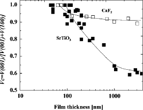
Figure 2 shows V c evolution as function of film thickness for films grown on both (100)cSrRuO3//(100)LaNiO3//(100)CaF2 and (100)cSrRuO3//(100)SrTiO3 substrates. We notice that V c value is unity when the film is thin and decreases with increasing film thickness. However, V c value is limited at ∼0.9 for thicknesses greater than 200 nm in the case of films grown on CaF2 substrates as shown on Fig. 2. This V c value from CaF2 substrates is larger than that for SrTiO3 substrates (V c = 0.6) due to the larger thermal strain on CaF2 compared to that on SrTiO3 above the Curie temperature.
c-domain volume fraction (V c) versus film thickness for PbTiO3 films grown on CaF2 (□) and on SrTiO3(■) substrates.

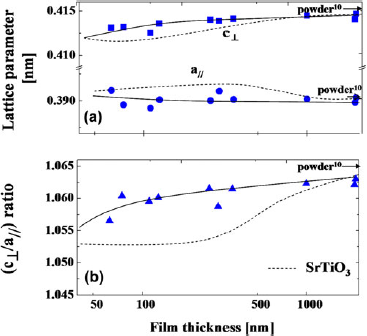
Figure 3(a) shows film thickness dependency of out-of-plane c-axis lattice parameter (c ┴) and in-plane a-axis lattice parameter (a //) and Fig. 3(b) shows their ratio (c ┴/a // ratio) for (001)-oriented domains. c ┴ and a // are the lattice parameters of the (001)-oriented domain with the polar axis along the surface normal direction. The (001)-oriented domains are expected to mainly contribute to the ferroelectricity of the present films. The dashed line on Fig. 3 shows the reported values for films grown on (100)SrTiO3 substrates, already reported by our group,Reference Nakaki, Kim, Yokoyama, Ikariyama, Nishida, Saito and Funakubo 23 as well as the reported data for the strain-free powders.Reference Shirane and Hoshino 25 The lattice parameters of the a- and c-axes decreased and increased, respectively, as the film thickness increased. Moreover, the lattice parameters for the a- and c-axes are saturated to similar values as those reported for powders.Reference Shirane and Hoshino 25 Additionally, the c ┴/a // ratio increased and approached to the powders as the film thickness increased. As shown in Fig. 3(b), lattice parameters and the c ┴/a // ratio on CaF2 substrates are closer to the reported powder data than those on SrTiO3 substrates. This result suggests a smaller residual strain on CaF2 substrates compared to SrTiO3 substrates. It is must be noted here that there is no evident influence of film quality on electrical properties. These results will be discussed later. Film quality is estimated by rocking curve peak full-width at half-maximum measured on both substrates and at different thicknesses.
Film thickness dependency of (a) out-of-plane c-axis (c ┴) and in-plane a-axis (a //) lattice parameters and (b) c ┴/a // ratio for (001)-oriented domains for PbTiO3 films grown on CaF2 (■, ●, and ▲) and on SrTiO3 substrates (dashed lines).Reference Nakaki, Kim, Yokoyama, Ikariyama, Nishida, Saito and Funakubo 23 Powder dataReference Shirane and Hoshino 25 are also plotted for comparison.

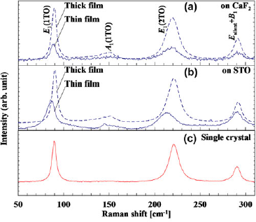
Figure 4 presents the Raman spectra of 300- and 2000-nm-thick PbTiO3 films deposited on CaF2 substrate [Fig. 4(a)] and SrTiO3 substrate [Fig. 4(b)]. Single crystal data are also plotted on Fig. 4(c) as a strain-free reference sample. It has been reported that E(TO) modes are the most reliable for estimating biaxial residual stressReference Bartasyte, Margueron, Kreisel, Bourson, Chaix-Pluchery, Rapenne-Homand, Santiso, Jimenez, Abrutis, Weiss and Fontana 26 ; thus, we monitored strain state of PbTiO3 films by examining E(TO) modes shifts with regard to relaxed sample spectrum. These figures allow us to notice that, depending on substrate, PbTiO3 films show a different strain state as a function of film thickness. Indeed, in case of CaF2 substrate [Fig. 4(a)], PbTiO3 films show a negligible residual strain as the Raman peaks are almost aligned on strain-free state peaks, independently from film thickness. On the other hand, thin films grown on SrTiO3 substrate present shifts of E(TO) mode due to strain in thin film sample. This strain is released in the thick film samples and approaches single crystal data, suggesting that strain relaxation occurs when PbTiO3 thickness increases. These results are in good agreement with XRD data presented on Fig. 3 and show the presence of larger residual stress in thin films deposited on SrTiO3 substrates.
Raman spectrum of films with 300 and 2000 nm in thickness for films prepared on (a) CaF2 substrates and (b) SrTiO3 substrates. PbTiO3 single crystal data is shown in (c).

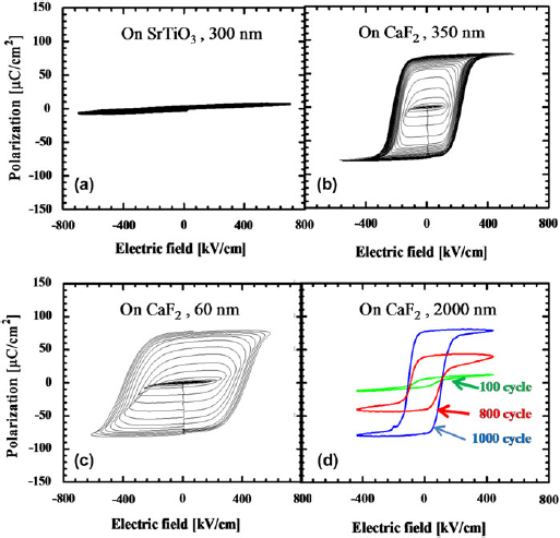
Figure 5 shows the room temperature polarization–electric field (P–E) hysteresis loops measured at 100 kHz for PbTiO3 films deposited on SrTiO3 substrate [Fig. 5(a)] and on CaF2 substrates [Figs. 5(b)–5(d)].
In the case of PbTiO3 film grown on SrTiO3 substrate, ferroelectricity is not observed. This might be ascribed to the strained state of the 300-nm-thick film studied in this work, as pointed out on Figs. 3 and 4. Indeed, misfit strain during film growth and thermal strain induced during cooling process are possible root causes.
Polarization versus electric field (P–E) hysteresis loops measured at 100 kHz for PbTiO3 films deposited on SrTiO3 (a) and on CaF2(b–d). Film thickness: (a) 300 nm, (b) 350 nm, (c) 60 nm, and (d) 2000 nm.

Thermal strain (εt) depends on substrate thermal expansion coefficient, αsub Reference Fujisawa, Nakaki, Ikariyama, Morioka, Yamada, Saito and Funakubo 18 :
 $${\rm{\varepsilon }}_{\rm{t}} = ({\rm{\alpha }}_{{\rm{sub}}} - {\rm{\alpha }}_{{\rm{film}}} )(T_{\rm{g}} - T_{\rm{c}} )\quad,$$
where αfilm is the thermal expansion coefficient of PbTiO3 films. T g and T c are growth and Curie temperatures, respectively.
For thick films, thermal strain becomes dominant. This thermal strain is induced under the Curie temperature during cooling process from high deposition temperature to room temperature. Hence, it has been demonstrated that decreasing thermal strain leads to decreasing c-domain volume fraction and increasing global internal stress.Reference Fujisawa, Nakaki, Ikariyama, Morioka, Yamada, Saito and Funakubo 18 The relatively lower thermal expansion coefficient of SrTiO3 (11.2 × 10⁻⁶ K−1) allows the apparition of c-domain (Fig. 2) and the presence of internal strain. This internal strain deforms PbTiO3 lattice parameter (Fig. 3).Reference Fujisawa, Nakaki, Ikariyama, Morioka, Yamada, Saito and Funakubo 18
On the other hand, the influence of internal strain on ferroelectric characterization can also be emphasized by the increase of the Curie temperature (T C),Reference Li, Hu, Liu and Chen 20 associated with an increase of the coercive field (E c) beyond the dielectric strength. Indeed, if E c is larger than breakdown voltage (V BD) of our material, no hysteresis loop can be observed. Thus, an extremely large coercive field might be a good explanation for the absence of ferroelectricity in PbTiO3 films deposited on SrTiO3 substrate.
In contrast, in the case of PbTiO3 on CaF2 substrates, well-saturated hysteresis loops are observed regardless of the film thickness. Remnant and saturated polarization (P r and P sat) values are 73 and 84 μC/cm2, 76 and 78 μC/cm2, and 75 and 76 μC/cm2 for 60, 350, and 2000 nm, respectively. These changes are relatively small with regards to increasing film thickness, while the coercive field (E c) monotonously decreased with increasing film thickness.
This latter result is in agreement with reported data by Lee et al.Reference Lee, Nakhmanson, Chisholm, Christen, Rabe and Vanderbilt 19 Indeed, these authors pointed out that E c varies as function of film thickness (T ox) according to the following relationship:
 $$T_{{\rm{ox}}} \propto \hskip.4E_{\rm{c}}^{ - 2/3} \quad.$$
Thus, decreasing PbTiO3 thickness leads to an increasing of coercive field.
It must be mentioned that for thick film samples (over 1000 nm), full performance of PbTiO3 film could be reached by multiple cycling. Indeed, as shown on Fig. 5(d), 1000 measurement cycles are necessary to fully overcome pinning phenomena and thus achieve full performance of our film. This might be related to the switching mechanism of polarization; e.g., the difficulty of switched domains in penetrating thick films. Detailed explanations of this statement are under investigation.
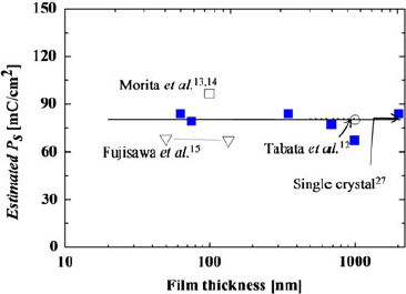
Figure 6 shows the thickness dependency of the estimated spontaneous polarization (P s, P s = P sat/V c) for PbTiO3 films on CaF2 substrates. It must be mentioned that micro-Raman spectroscopy indicated that (100)-oriented domains did not switch to (001) orientation under an applied electrical field, regardless of film thickness. Figure 6 also shows the reported values for epitaxial (100)/(001)-oriented PbTiO3 filmsReference Tabata, Murata, Kawai, Kawai and Okuyama 12 – Reference Fujisawa, Seioh, Kume and Shimizu 15 as well as those for a single crystal.Reference Venevtsev, Zhdanov, Solov’ev and Ivanova 27 The estimated P s in the present study for 60–2000-nm-thick films is almost constant and equal to ∼80 μC/cm2. The present P s values are nearly identical as the reported value of single crystal.Reference Venevtsev, Zhdanov, Solov’ev and Ivanova 27
Estimated P s (= P r/V c) as a function of film thickness for PbTiO3 films grown on CaF2 substrates (■). Reported P s for epitaxial (001)-oriented epitaxial PbTiO3 films by Tabata et al. (○),Reference Tabata, Murata, Kawai, Kawai and Okuyama 12 Morita et al. (□),Reference Morita and Cho 13 , Reference Morita and Cho 14 and Fujisawa et al. (∆)Reference Fujisawa, Seioh, Kume and Shimizu 15 are also shown as well as reported one for a single crystal.Reference Venevtsev, Zhdanov, Solov’ev and Ivanova 27

This is considered to be related to the small residual strain of the present films grown on CaF2 substrates compared to the conventional epitaxial films on SrTiO3 substrates. Present results also indicate the usefulness of CaF2 substrates for the growth of highly (001)-oriented tetragonal Pb(Zr,Ti)O3 films with small residual strain.
IV. CONCLUSIONS
(100)/(001)-oriented epitaxial PbTiO3 films with various film thicknesses are grown on (100)cSrRuO3-covered CaF2 and SrTiO3 substrates by pulsed MOCVD. V c value of the films decreased from 1 to 0.9 as film thickness increased. Large P r value above 60 μC/cm2 is observed for a wide range of the film thickness from 60 to 2000 nm. The estimated P s value is about 80 μC/cm2, which agrees well with the measured value from the polar axis-oriented epitaxial tetragonal Pb(Zr,Ti)O3 films as well as the reported value of the single crystal.
ACKNOWLEDGMENT
This work was partially supported by Grants-in-Aid from the Ministry of Education, Culture, Sports, Science and Technology, Japan, for the Elements Science and Technology Project (Grant Nos. 21360316 and 20047004) and the Japanese Society for the Promotion of Science (JSPS).