I. INTRODUCTION
Nanowires and nanotubes have wide range of potential applications, such as chemical and optical sensors,Reference Sirbuly, Tao, Law, Fan and Yang1, Reference Choi, Hwang, Park, Choi, Park and Lee2 resonators and force sensors,Reference Dobrokhotov, Yazdanpanah, Pabba, Safir and Cohn3, Reference Li, Bhiladvala, Morrow, Sioss, Lew, Redwing, Keating and Mayer4 high-resolution scanning probe microscope (SPM) tips,Reference Tay and Thong5 and reinforcements for nanocomposites.Reference Bao and Tjong6, Reference Ajayan, Schadler and Braun7 To design the devices composed of these nanomaterials, it is essential to know their behavior and properties, e.g., mechanical properties for the applications of force sensors, SPM tips, and nanocomposites. Mechanical characterization at such small scales is very challenging.
Nanoindenter and atomic force microscope have been successfully used to laterally indent nanowires and nanotubes,Reference Li, Nardi, Baek, Kim and Kim8–Reference Ni and Li18 whereas the associated rigorous analytical solution is not available due to the complex contact mechanics.Reference Feng, Nix, Yoon and Lee9 Consequently, approximations were made in these previous studiesReference Li, Nardi, Baek, Kim and Kim8–Reference Ni and Li18 to proceed with indentation data analysis. However, some of the approximations may be problematic: (i) treating the nanomaterial as half-space (using the Oliver–Pharr methodReference Oliver and Pharr19 for data analysis),Reference Li, Gao, Murphy and Caswell10, Reference Fang and Chang14, Reference Mao, Zhao and Wang15 (ii) neglecting the contact deformation between the nanomaterial and substrate,Reference Yu, Kowalewski and Ruoff11, Reference Tan and Lim16 and (iii) neglecting the possibility of receding (the ends of the nanomaterial being separated from the substrate).Reference Li, Nardi, Baek, Kim and Kim8, Reference Li, Gao, Murphy and Caswell10–Reference Ni and Li18 To take account of the aforementioned effects, Feng et al. have proposed a double-contact (two contacts in series) modelReference Feng, Nix, Yoon and Lee9: contact 1 (indenter/nanowire) is approximated by a Hertzian elliptical contact of sphere/cylinder, and, contact 2 (nanowire/substrate) is approximated by a receding contact of cylinder/half-space. The Hertzian elliptical contact has a closed-form solution.Reference Johnson20 Although the receding contact of cylinder/half-space does not have a rigorous analytical solution, a mechanism-based analytical approximation was empirically derived.Reference Feng, Nix, Yoon and Lee9 However, to our best knowledge, all previous analytical models and data analysisReference Li, Nardi, Baek, Kim and Kim8–Reference Ni and Li18 on nanowire lateral probing have not been quantitatively compared to numerical models, e.g., finite element analysis (FEA).
In this article, a quantitative physical picture, first time in the literature, is proposed to model the lateral probing of a nanowire, which is used to analyze a three-dimensional (3D) FEA, and the results are compared with that based on the double-contact model.Reference Feng, Nix, Yoon and Lee9
II. FEA MODELING
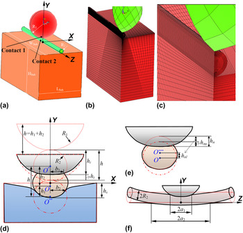
As shown in Fig. 1(a), a 3D FEA model is developed using ANSYS 11 for lateral probing of a GaN nanowire on a Si substrate. Again, to our best knowledge, none of previous studiesReference Li, Nardi, Baek, Kim and Kim8–Reference Ni and Li18 have quantitatively compared the analytical or experimental results with the FEA results. Since purely elastic contact modeling would already provide significant physical insights, and moreover all previous analytical modelsReference Li, Nardi, Baek, Kim and Kim8, Reference Li, Gao, Murphy and Caswell10–Reference Ni and Li18 for nanowire lateral probing are supposed to be suitable for purely elastic contact, so that in the study, isotropic elasticity is assumed with E GaN = 301 GPa, ν GaN = 0.26, E Si = 162 GPa, and ν Si = 0.22.Reference Feng, Nix, Yoon and Lee9 Here, E represents Young’s modulus, and ν represents Poisson’s ratio.
A model of a lateral nanowire indentation. (a) The geometry, the coordinate system, and the associated parameters. (b) The FEA model. (c) A magnification of (b). (d)–(f) The schematics of a physical picture of nanowire indentation. In (d)–(f), the solid shapes are in the deformed configuration, and the dotted shapes are in the undeformed configuration. (d) A schematic at the X–Y plane, where the dash-dot shape is an undeformed indenter shape with its top overlapping with the top of the indenter in the deformed configuration, and the dash-double-dot circle is an undeformed nanowire shape (centered at O**) with its top touching the undeformed indenter shape (the dash-dot shape). Here, O is the mass-center of the deformed nanowire, and O* is the nanowire center in the undeformed configuration. (e) A partial replot of (d), where two undeformed nanowire shapes are also drawn: (i) a dash-dot circle centered at O, and (ii) a dotted circle (centered at O***) with its bottom overlapping with the bottom of the deformed nanowire. (f) A schematic at the Y–Z plane. In schematics (d)–(f), a deformable indenter is assumed for generality, and the shapes are not in scale.

A spherical indenter is assumed to be rigid for simplicity with a radius of R 1= 200 nm. The nanowire radius R 2 = 33 nm. The nanowire length (40R 2) and the substrate dimensions (20R 2 × 20R 2 × 40R 2) are taken much larger than R 2. The indenter/nanowire and nanowire/substrate contacts will be referred as contacts 1 and 2, respectively. Only one quarter of the set up in Fig. 1(a) is modeled due to the symmetry. Contacts 1 and 2 are modeled as surface-to-surface contacts.21 Contact 1 is frictionless. To study the adhesion effect, two limiting cases at contact 2 are modeled: (i) frictionless and freely separable, referred as the receding case, and (ii) bonded along the line initially in contact and frictionless elsewhere, referred as the bonded case. Figures 1(b) and 1(c) show the mesh used in the FEA model. A further mesh refinement with half mesh size results in a less than 5% difference in the indentation load P, indicating a good mesh convergence.
III. QUANTITATIVE PHYSICAL PICTURE
The quantitative physical picture of lateral probing of a nanowire should be first understood to provide quantitative analysis, which, however, has never been done adequately in the literature.Reference Li, Nardi, Baek, Kim and Kim8–Reference Ni and Li18Figures 1(d)–1(f) illustrate a physical picture, showing various parameters including b 1 and b 2, the minor radii of contacts 1 and 2, respectively; a 1 and a 2, the major radii of contacts 1 and 2, respectively; h, the indentation depth; h i, the displacement of the initial contact point; h t, the indenter-tip deformation (h t = 0 for a rigid indenter); h s, the substrate deformation; h n, the nanowire deformation (the nanowire top-to-bottom relative displacement); h nu, the nanowire upper-part deformation; and h nl, the nanowire lower-part deformation. The upper and lower parts of the nanowire may be divided by its mass-center O. According to Figs. 1(d) and 1(e),

The contact deformation of contact 1, referred as h 1, may be estimated by summing the tip deformation h t and the nanowire upper-part deformation h nu, i.e.,

Similarly, the contact deformation of contact 2, referred as h 2, may be estimated by summing the nanowire lower-part deformation h nl and the substrate deformation h s, i.e.,

Thus, according to Eqs. (1)–(3),

which is expected on the basis of the double-contact (two contacts in series) model.
In our FEA modeling, h is the controlling input, h 2 can be measured by the displacement of the nanowire mass-center [see Fig. 1(d)], and then h 1 ≈ h − h 2 according to Eq. (4).
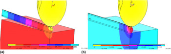
Although the physical picture as shown in Figs. 1(d)–1(f) is obvious, according to our best knowledge, the contact 2 deformation h 2 was completely ignored in all previous reportsReference Li, Nardi, Baek, Kim and Kim8–Reference Ni and Li18 on lateral nanowire/nanotube indentation except in the Feng study.Reference Feng, Nix, Yoon and Lee9 However, h 2 could be pronounced especially for a relatively compliant substrate. For example, h 2 ≈ 60%h according to our FEA results [see Figs. 2(a) and 2(b)].
The finite element analysis (FEA)-determined Y-displacement fields in the deformed configuration at h = 12 nm. (a) The receding case. (b) The bonded case.

IV. RESULTS AND DISCUSSIONS
A. Calculation of the FEA-determined and analytical results
Figure 2(a) shows the Y-displacement (see Fig. 1 for the coordinate system) field for the receding case at h = 12 nm (P = 49.8 μN), indicating a significant nanowire receding. Figure 2(b) shows the Y-displacement field for the bonded case at h = 12 nm (P = 53.6 μN), indicating a nanowire/substrate bonding situation.
All parameters shown in Figs. 1(d) and 1(e) can be directly measured or calculated from the FEA simulations. On the other hand, according to the Feng model,Reference Feng, Nix, Yoon and Lee9 if we know the elastic constants as well as the radii of nanowire and indenter, the load P and the elastic contact stiffness S (= d P/dh due to purely elastic FEA modeling) are necessary and sufficient for estimating the nanowire hardness H. Here, the stiffnesses for contacts 1 and 2 (S 1= dP/dh 1 and S 2= dP/dh 2) as well as the contact radii can be calculated as analytical intermediate results. Thus, by comparing the FEA-determined results and the intermediate and final results based on the analytical model, we can verify the basic assumptions as well as the validity of the analytical model.
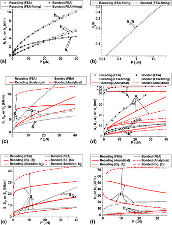
Figures 3(a)–3(f) plot the FEA-determined and analytical results, where the analytical results are calculated from P and S according to the analytical solution in the Feng study.Reference Feng, Nix, Yoon and Lee9 Here, to achieve a better comparison, the coefficient β′ in Eqs. (6) and (8) in the Feng studyReference Feng, Nix, Yoon and Lee9 is recalibrated to be 1.0 (not 2.87 in the original Feng solutionReference Feng, Nix, Yoon and Lee9). Here, β′ is a geometry coefficient for receding problems,Reference Feng, Nix, Yoon and Lee9 which depends almost only on the contact geometry, e.g., β′ = 1.0 for any plane contacts and β′ = 1.3 for any axisymmetric contacts. Feng et al.Reference Feng, Nix, Yoon and Lee9 originally estimated β′ = 2.87 based on the solely available analytical report by Castillo and BarberReference Castillo and Barber22 on the contact between a cylinder and a rigid half-space.Reference Castillo and Barber22 However, β′ = 2.87 may not be good for a stiff cylinder on a compliant substrate, e.g., the GaN-wire/Si-substrate case in this study. Therefore, based on the relation between the FEA-determined a 1 and a 2, we recalibrate and find β′ = 1.0, indeed interestingly matching the value for the receding plane contact, as expected for the nanowire/substrate contact along the nanowire-axis direction.
The parameters plotted versus P, where the FEA results are black symbols or thin black lines, and the analytical results are thick red lines. Here, the thin lines are (or are based on) the fittings of the FEA results. (a) h, h 1, and h 2. (b) h 2/h. (c) S, S 1, and S 2. (d) a 1, a 2, b 1, and b 2. (e) S 1 and S 2, where the lines corresponding to “Sneddon, b 2” are virtually the same. (f) H 1 and H 2, where the lines corresponding to Eq. (7) are virtually the same.

B. Analysis of the FEA-determined results
To have a clear discussion, in this section, we focus only on the FEA-determined results, and the comparison between the FEA-determined and analytical results are discussed in the next section.
In Figs. 3(a)–3(f), the FEA-determined results are shown as thin black solid lines (the receding case) and thin black dash-dot lines (the bonded case). The subscript indicates the contact (contacts 1 or 2) to which the quantity is related to.
Figures 3(a)–3(d) indicate that, for each FEA-determined parameter, there is only a tiny discrepancy between the receding and bonded cases, implying that the adhesion condition at contact 2 has a small effect. Figure 3(b) indicates h 2/h > 10% for P > 0.1 μN, where 0.1 μN is the resolution of most commercial nanoindenters; consequently, it is problematic to ignore h 2, especially for compliant substrates, as in some previous studies.Reference Yu, Kowalewski and Ruoff11, Reference Tan and Lim16
Figure 3(c) shows the stiffnesses, indicating that S 1 quickly increases with increasing P, whereas the increase of S 2 is not as significant; if P > 5 μN, S 1 > S 2, i.e., contact 2 is more compliant, and again we cannot ignore contact 2. Moreover, S 2 jumps to about 4 kN/m at P = 0.1 μN in both the receding and bonded cases as expected for a receding-like contact 2.Reference Feng, Nix, Yoon and Lee9 Furthermore, the overall stiffness S is less than S 1 and S 2, as expected for the double contacts in series.
Figure 3(d) shows the contact radii, where a 2 in the bonded case is determined by the position at which the stress σYY changes sign.Reference Feng, Nix, Yoon and Lee9Figure 3(d) shows that for P > 10 μN, a 2 keeps constant in both the receding and bonded cases, implying that contact 2 is receding-like along the nanowire-axis direction.Reference Feng, Nix, Yoon and Lee9, Reference Castillo and Barber22Figure 3(f) shows the mean pressures calculated by H ≈ P/πab, indicating H 1 > H 2 as expected. It is surprising to see that even for a purely elastic contact 1, H 1 reaches a plateau for P > 10 μN, which may be due to the stress relaxation from the traction-free surface of the nanowire.Reference Xu and Li23
C. Comparison of the FEA-determined and analytical results
In the following, we want to compare the FEA and analytical (the thick red lines) results. Here, the analytical results are calculated from the FEA-determined P and S according to the solution in the Feng study.Reference Feng, Nix, Yoon and Lee9
In Fig. 3(d), because of the recalibration of β′ as mentioned before, the analytical a 2 in the receding case matches well with the corresponding FEA result. It is surprising to see that the analytical a 2 in the bonded case also matches with the corresponding FEA result very nicely. However, in both the receding and bonded cases, Fig. 3(c) shows that the analytical solution largely underestimates S 1 but overestimates S 2, and Fig. 3(d) shows that the analytical solution largely underestimates a 1 and b 1, whereas Fig. 3(f) shows that the analytical solution largely overestimates the nanowire hardness H 1. The multifold reasons for these discrepancies are discussed in the following.
The dominant reason is that the contact-pressure distribution at contact 2 was assumed in the analytical model to be similar to a Hertzian distribution at an elliptical contact,Reference Johnson20 so that the Hertzian formula was used for estimating S 2,Reference Feng, Nix, Yoon and Lee9 i.e.,

where E r is the reduced modulus,Reference Feng, Nix, Yoon and Lee9a and b are the major and minor radii, and λ is a parameter depending on b/a [see Eq. (2b) in the Feng studyReference Feng, Nix, Yoon and Lee9]. To verify this reason, namely Eq. (5) is not good for contact 2, based on the FEA-determined a 2 and b 2, S 2 is calculated using Eq. (5) and plotted in Fig. 3(e) [see Eq. (5) in the legend] for the receding and bonded cases, indicating that Eq. (5) largely overestimates S 2.
This overestimation of S 2 by Eq. (5) is because the contact-pressure at contact 2 is too strongly concentrated to be described by a Hertzian distribution. To verify this strong stress concentration at contact 2, we may approximate contact 2 by an axisymmetric contact with its radius equal to the minor radius b 2, so that the Sneddon solution can be used for estimating S 2,Reference Feng, Nix, Yoon and Lee9, Reference Oliver and Pharr19, Reference Pharr, Oliver and Brotzen24 i.e.,

where b is the contact radius of the circular contact.Reference Pharr, Oliver and Brotzen24 Based on the FEA-determined b 2, the S 2 calculated using Eq. (6) is plotted in Fig. 3(e) (see “Sneddon, b 2” in the legend), indicating that the Sneddon solution estimates (slightly underestimates) S 2 fairly well, especially for large P. Therefore, the Sneddon solution based on the minor radius of contact 2 provides a good lower bound for estimating S 2.
Thus, in summary, these discrepancies between the FEA and analytical results due to the dominant reason can be explained as follows. When the Feng solution is used based on P and S, S 2 would be overestimated by Eq. (5), so S 1 would be underestimated due to 1/S = 1/S 1 + 1/S 2 as shown in Fig. 3(c). Consequently, when we apply Eq. (5) to contact 1, namely  ,Reference Feng, Nix, Yoon and Lee9 to find out a 1 and b 1, they would be underestimated as shown in Fig. 3(d) because of the underestimation of S 1. Therefore, H 1 (≈P/πa 1b 1) is overestimated, as shown in Fig. 3(f).
There is another discrepancy between the FEA and analytical H 1 results as shown in Fig. 3(f), namely, with increasing P, the FEA-determined H 1 increases, whereas the analytical H 1 decreases. The dominant reason for this discrepancy is that Eq. (5) is not good for contact 1 either, although Eq. (5) (the Hertzian elliptical contact equation) has been used for modeling nanowire and nanotube indentations in the Feng study and several other previous studies.Reference Feng, Nix, Yoon and Lee9, Reference Yu, Kowalewski and Ruoff11, Reference Lonnroth, Muhlstein, Pantano and Yue17 To verify this, based on the FEA-determined a 1 and b 1, S 1 can be calculated using Eq. (5) and plotted in Fig. 3(e) [see Eq. (5) in the legend] for the receding and bonded cases, indicating that the S 1 calculated by Eq. (5) does not match nicely with the FEA-determined S 1. This invalidity of Eq. (5) for contact 1 is due to the fact that Eq. (5) is derived based on small deformation,Reference Johnson20 i.e., h 1 ≪ R 2 and b 1 ≪ R 2, whereas b 1/R 2 > 10% for P > 1 μN as shown in Fig. 3(d), i.e., the small deformation condition is not satisfied.
In fact, noticing that  according to Eq. (5), we can estimate the contact pressure H for an Hertzian elliptical contact by
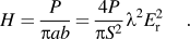
To further verify that Eq. (5) is not good for contact 1, based on the FEA-determined S 1 and λ 1 (from the FEA-determined a 1 and b 1Reference Feng, Nix, Yoon and Lee9), H 1 is calculated using Eq. (7) and plotted in Fig. 3(f) [see Eq. (7) in the legend], indicating that the H 1 calculated using Eq. (7) decreases with increasing P, and this decreasing trend is opposite to that of the FEA-determined H 1.
Therefore, we can conclude that Eq. (5) which is for Hertzian elliptical contactReference Johnson20 cannot well describe contact 1, although the Hertzian contact theory has been widely used in the most advanced published modelsReference Feng, Nix, Yoon and Lee9, Reference Yu, Kowalewski and Ruoff11, Reference Lonnroth, Muhlstein, Pantano and Yue17 for nanowire and nanotube indentations. As a future work, we would determine the upper limits of contact dimensions under which Hertzian elliptical contact theory can be applied and also provide a better theory (if analytically possible) being valid for large deformation.
V. CONCLUSIONS
In this study, to verify an analytical solution for lateral nanowire indentation, 3D FEA is performed on the basis of pure elasticity for a specific case: a spherical indention of a GaN nanowire on a Si substrate, showing significant deformation at contact 2 (the nanowire/substrate contact). Thus, it is problematic to ignore the deformation at contact 2, as in almost all previous studies. Moreover, the FEA modeling for the GaN-nanowire/Si-substrate case indicates that the adhesion condition at contact 2 (the nanowire/substrate contact) has a very small effect, and that contact 2 is receding-like along nanowire-axis direction. In addition, the mean pressure at contact 1 (the indenter/nanowire contact) reaches a plateau for large-enough indentation load.
Also, although the analytical solution can generally and qualitatively describe the FEA-determined results, there are discrepancies between the FEA and analytical results, which are mainly due to two reasons. The first reason is that the contact-pressure distribution at contact 2 is much more concentrated than that described by a Hertzian elliptical distribution. The second reason is that contact 1 cannot be well described by a Hertzian elliptical contact because of large contact deformation.
ACKNOWLEDGMENT
The authors acknowledge the financial support from a Keystone Innovation Starter Kit (KISK) grant from the Pennsylvania Department of Community and Economic Development.