For structural characterization of nanocrystalline and amorphous materials, imaging by transmission electron microscopy (TEM) with high spatial resolution and elemental contrast is a standard technique. It is therefore of general interest for the community of material science to know if their materials are susceptible for the artifacts the energetic electron irradiation during TEM studies may evoke.[Reference Egerton, Li and Malac1, Reference Hobbs, Clinard, Zinkle and Ewing2] The artifacts have been reported both as amorphization of crystalline materials[Reference Bae, Ishimaru and Hirotsu3, Reference McCartney, Crozier, Weiss and Smith4] and crystallization of amorphous materials,[Reference Jenčič, Bench, Robertson and Kirk5, Reference Nagase, Sanda, Nino, Qin, Yasuda, Mori, Umakoshi and Szpunar6] depending on electron energy, dose, and the type of material. These sample artifacts may be due to processes such as atomic displacement, radiolysis, and sample heating.[Reference Egerton, Li and Malac1, Reference Hobbs, Clinard, Zinkle and Ewing2, Reference Williams and Carter7]
An important class of materials is metal carbides. These have wide stoichiometry ranges and exhibit several crystal structures that often form nanocomposites when rich in carbon. More elements are added to tailor the materials for, e.g., tribological or electrical applications.[Reference Martínez-Martínez, López-Cartes, Fernández and Sánchez-López8–Reference Eklund, Emmerlich, Högberg, Wilhelmsson, Isberg, Birch, Å Persson, Jansson and Hultman11] For example, thin films of the Ti–Si–C system can be grown with a nanocomposite structure consisting of TiC crystallites embedded in an amorphous matrix of SiC and C.[Reference Eklund12–Reference Lauridsen, Eklund, Joelsson, Ljungcrantz, Öberg, Lewin, Jansson, Beckers, Högberg and Hultman14] Amorphous (glass-like) structures are also reported to form in Me–Si–C systems (e.g., for the metals Me = Ti,[Reference Naka, Sakai, Maeda and Mori15] Zr,[Reference Kádas, Andersson, Holmström, Wende, Karis, Urbonaite, Butorin, Nikitenko, Kvashnina, Jansson and Eriksson16] Mo,[Reference Krzanowski and Wormwood17] and W[Reference Endrino and Krzanowski18]). For TEM characterization of these complex-structure materials, it is essential to find not only imaging conditions, but also sample preparation methods that allow characterization of the true nature of the material. Correspondingly, one should elucidate any electron-beam/sample interaction including possible crystallization.
Here, we report the effects of electron beam interactions with dc magnetron sputtered Me–Si–C thin films with amorphous structure during TEM analysis. Since the only observable interactions are under high-resolution (HR-)TEM conditions, this study uses the technique both to induce artifacts and observe them. The metal (Me) was selected from group 4 (Zr) and group 5 (Nb) in the periodic table. We separate between different damage effects by imaging the sample at different current densities and acceleration voltages. The effects of sample heating by in situ annealing are also investigated. Comparing the nanocrystalline fraction from HRTEM images can be challenging due to, e.g., unknown sample thicknesses and different defocusing conditions. However, we are here able to qualitatively separate different damage effects. The results show that the amorphous phase of both material systems is unstable to exposure of the HRTEM electron beam, which induces MeC crystallization. Low-dose electron exposure, however, offers a way to better determine their structure.
Experimental
Thin films of Me–Si–C (Me = Nb or Zr) were deposited from elemental targets using dc magnetron sputtering in an Ar discharge. A detailed description of the deposition process, together with compositional and structural characterization for Nb–Si–C and Zr–Si–C can be found in Refs. Reference Nedfors, Tengstrand, Flink, Eklund, Hultman and Jansson19 and Reference Andersson, Urbonaite, Lewin and Jansson20 respectively.
Cross-sectional specimens were obtained by mechanically polishing down to ~50 µm followed by ion milling (at 5° incidence angle) in a Gatan Precision Ion Polishing System (PIPS) using 5 keV Ar+ ions. As a final step, the samples were polished with 2 keV Ar+ ions. Ion-milling involves potential damage to the material. For the present class of materials, Lewin et al.[Reference Lewin, Gorgoi, Schäfers, Svensson and Jansson21] found that etching Ti–Me–C (Me = Al, Fe, Cu, Pt, or Ni) films with 4 keV Ar+ ions altered the chemical bonding observed in XPS. The same energy-range (~1–5 keV) is used during ion-milling in the TEM sample preparation. Thus, in order to exclude any possible damage effects from ion radiation, the small angle cleavage technique (SACT)[Reference Walck and McCaffrey22] was used on the Nb0.10Si0.39C0.51 sample. This sample was polished down from the substrate side to a thickness of ~70 µm followed by cleavage at a small angle (~17°) to the edge, creating a very thin region at the interface. The technique guarantees radiation damage-free samples, albeit relatively small regions will be electron transparent.[Reference McCaffrey23]
TEM experiments were carried out in a FEI Tecnai G2 TF 20 UT instrument with a field-emission gun operated at acceleration voltages of 200 and 80 kV. The electron beam current was estimated by measurement of a focused beam on the fluorescent viewing screen. By setting the spot size and the exposure time, the current density and the electron dose could be calculated.
For the annealing experiment, a heating sample holder was used. First, the set-point temperature was put to 350 °C and held until the drift of the sample had stabilized. The temperature was then kept for additional 20 min before an image was acquired. This procedure was then repeated for new set-points of 400 and 600 °C. For the 600 °C heating experiment, the sample had to be cooled down to 400 °C before an image could be taken due to vibrations from external water-cooling of the rest of the sample holder.
Results and discussion
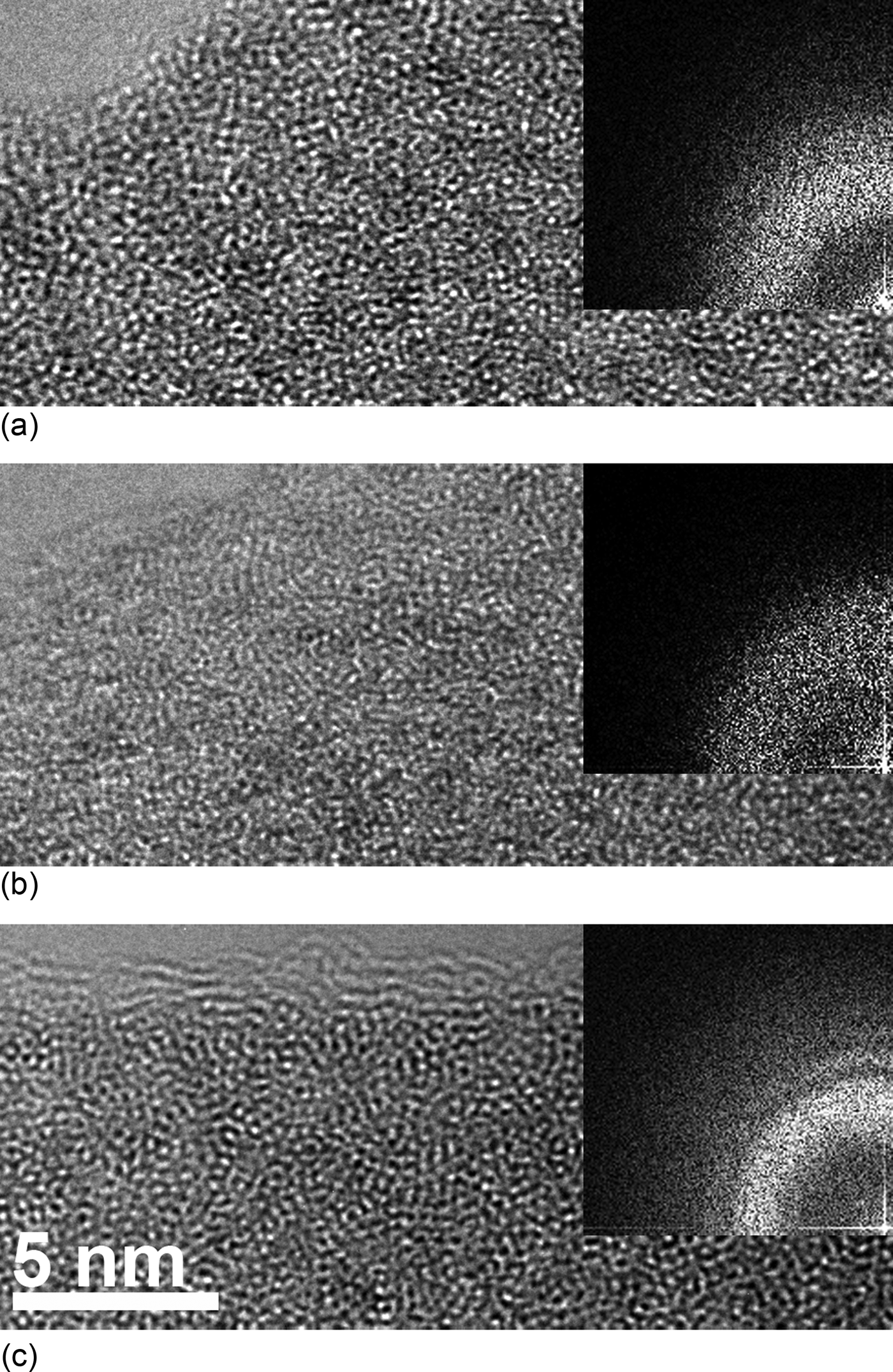
Figure 1 shows TEM images of (a) and (b) Nb0.10Si0.39C0.51, and (c) Zr0.43Si0.30C0.27 samples from direct imaging by rapid beam shift to a previously non-exposed area (i.e., the as-deposited state). The samples in (a), (c) are prepared with ion-milling, while the sample in (b) is prepared with SACT. All of the specimens exhibit amorphous structures with only some short-range ordering present. Since no considerable difference can be found between the SACT and the ion-milled sample, we conclude that ion-milling during sample preparation does not affect the samples significantly. The amorphous structure is also supported by selected area electron diffraction (not shown) taken over a larger area of the film. Hence, both materials are amorphous in their as-deposited state.
HRTEM images of the as-deposited Nb0.10Si0.39C0.51, prepared by ion milling and SACT in (a) and (b), respectively, (c) Zr0.43Si0.30C0.27 prepared by ion milling.

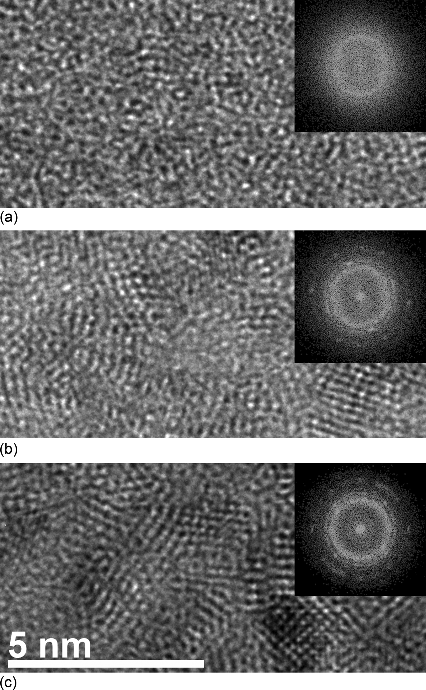
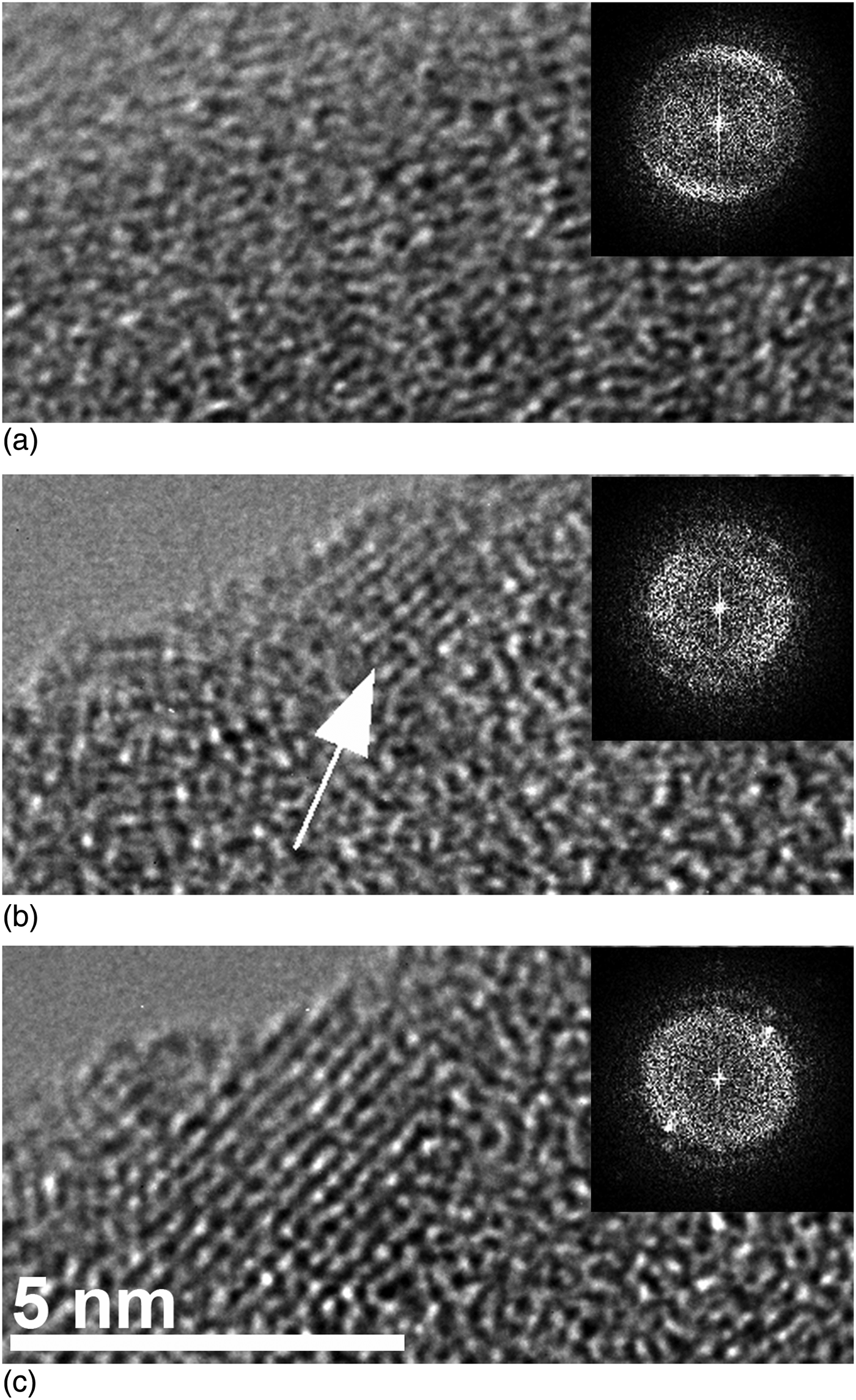
Crystallization of our samples started during HRTEM imaging. Quantitative comparisons between crystallized specimens can be difficult since it acquires knowledge of specimen thickness and some crystallites might also appear amorphous due to their orientation. However, if all of the specimens are prepared in the same way and the images are taken at the edge of the films (i.e., thickness approximately the same), the initial conditions are the same and a qualitative comparison is possible. In this article, we thus, qualitatively determined the amount of crystallization by comparing the number of observable crystalline grains formed and their size between different experimental treatments of the specimens. Figure 2 shows the structure evolution of the Nb0.10Si0.39C0.51 film from (a) as-deposited state to (b) and (c) different beam currents of 1.2 and 9.1 nA, respectively, for the same electron dose of ~2.8 × 10⁹ e−/nm2. Both (b) and (c) show a similar state of crystallization consisting of equiaxed crystallites with a diameter of ~2–5 nm. The diffraction patterns from the crystallized grains appearing in the FFT [insets Figs. 2(b) and 2(c)] agree well with that expected for an fcc structure. The best match for the lattice parameter (4.44 Å with standard deviation of ±0.03 Å as calculated from the micrograph) is NbC [4.46 Å (ICDD, PDF card 65-7964)]. The calculated lattice parameter is within error of the measurement, but the fact that the measured lattice parameter is smaller indicates that the crystallized NbC is understoichoimetric on C. The similar state of crystallization in Fig. 2(b) and 2(c) shows that the crystallization process is dose dependent. For Zr0.43Si0.30C0.27, the same dose (~2.8 × 10⁹ e−/nm2) shown in Fig. 3(b) does not affect the film as much as in the Nb–Si–C case. Only one grain in the thinnest part of the specimen (indicated by arrow) can be observed. After a longer exposure time (dose ~4.7 × 10⁹ e−/nm2) the Zr0.43Si0.30C0.27 also crystallized [Fig. 3(c)]. Similar to the Nb0.10Si0.39C0.51 film, the crystallites are equiaxed with a diameter of ~2–5 nm. The structure (fcc) and the calculated lattice parameter (4.70 Å with standard deviation of ±0.02 Å) are in agreement to that of ZrC [lattice parameter 4.69 Å (ICDD, PDF card 35-0784)]. A reason for the need of higher dose rates in the crystallization process of Zr–Si–C compared to Nb–Si–C could be the larger atomic radius of Zr, which from metallic glasses is known to stabilize the amorphous structure when mixed with elements of smaller atomic radii.[Reference Inoue and Takeuchi24]
HRTEM images of the Nb0.10Si0.39C0.51 film in as-deposited state (a) and (b) and (c) after exposure to a dose of ~2.8 × 10⁹ e−/nm2 for different beam currents of 1.2 and 9.1 nA, respectively.
HRTEM images with corresponding FFT insets of the Zr0.43Si0.30C0.27 film in an as-deposited state (a), and, after exposure to a dose of ~2.8 × 10⁹ e−/nm2 (b), and ~4.7 × 10⁹ e−/nm2 (c). The arrow in (b) marks a small crystalline grain.
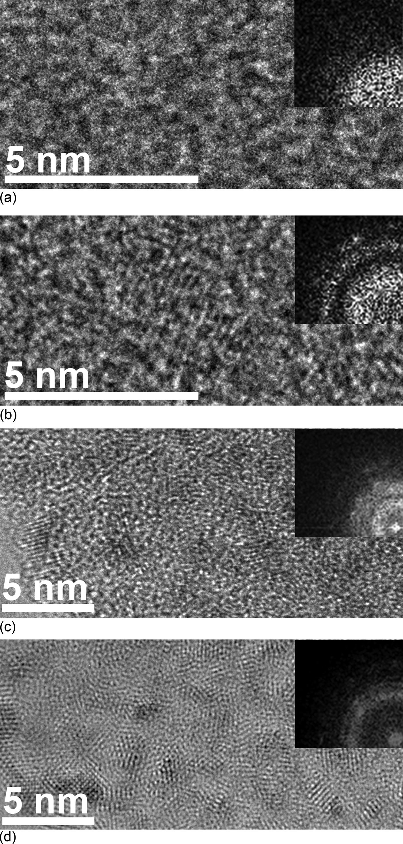
Heating of the sample can be excluded as the main explanation for crystallization based on the following annealing experiments. Electron-beam heating depends on several parameters of the sample, such as thermal conductivity and thickness, as well as properties of the beam, e.g., current and beam radius. To first order, the temperature increase can be approximated as proportional to the beam current through the specimen.[Reference Hobbs25] Williams and Carter[Reference Williams and Carter7] give general examples of this for materials with different thermal conductivity. It was shown that at a beam current in the order of 10 nA (this work), the temperature rise is not expected to be higher than 100 K even for an insulator [thermal conductivity 0.1 W/(m · K)]. Figures 4(a) and 4(b) show TEM micrographs of the Nb0.10Si0.39C0.51 specimen after annealing for 20 min at 400 and 600 °C, respectively. At 400 °C, no evidence of crystallization can be seen, but at 600 °C small crystalline grains have started to form. This crystallization process is, however, much slower compared with the beam-exposure experiment (cf. Fig. 2).
HRTEM images with corresponding FFT insets (a) and (b) Nb0.10Si0.39C0.51 thermally heated to 400 and 600 °C, respectively. (c) and (d) Nb0.10Si0.39C0.51 exposed to irradiated electrons with an acceleration voltage of 80 and 200 kV, respectively.
Also, radiolysis can be excluded by the following experiment and line of arguments. In this process, an inelastic scattered electron excites an electron in the material to make an interband transition. Defects formed in the following recombination process can lead to increased atom mobility and induce density fluctuations, which may induce crystallization.[Reference Nagase, Sanda, Nino, Qin, Yasuda, Mori, Umakoshi and Szpunar6] Radiolysis depends on electron–electron interactions, which increase with decreased acceleration voltage. Figure 4(c) and 4(d) show the Nb0.10Si0.39C0.51 sample irradiated with the same dose but at 80 and 200 keV electrons, respectively. At 80 keV, the crystallization is remarkably reduced. This contradicts the statement that the crystallization process is caused by radiolysis.
Instead, atomic displacement is suggested to cause crystallization. Displacement is due to elastic scattering and occurs when the transferred energy (E T) is larger than the displacement energy (E d) for an atom. More energy can be transferred to the lighter elements and at higher beam electron acceleration voltages.[Reference Egerton, Li and Malac1] As seen in Figs. 4(c) and 4(d), higher electron energy causes more crystallization for the same dose. Since thermal heating is excluded, this indicates that atomic displacement is the main cause for crystallization. Further investigations are needed to determine which element or elements are displaced. It is nevertheless more likely to be C and/or Si since these elements are lighter and can gain more energy from a displacement event. The electron beam-induced atomic displacements will thus cause additional or alternative disorder in the amorphous material. These defects can be seen as density fluctuations and the atomic reconfiguration to neutralize the fluctuations can lead to the formation of crystalline clusters.[Reference Nagase, Sanda, Nino, Qin, Yasuda, Mori, Umakoshi and Szpunar6]
Conclusions
Amorphous Me–Si–C (Me = Zr or Nb) thin films made by magnetron sputtering tend to crystallize due to electron irradiation during TEM investigations. Thereby, metal carbide crystallites form in both Nb–Si–C and Zr–Si–C. The crystallization is primarily caused by atom displacements.
These findings emphasize the need for great care in imaging these kinds of materials for a correct structure characterization. This is preferably done by low-dose electron microscopy. Finally, in light of the here demonstrated electron-beam-induced crystallization, there is a need to revisit and critically assess literature on nanocrystalline carbide-based nanocomposites, in particular, when TEM results appear to contradict characterization by other techniques such as XRD and Raman spectroscopy. Furthermore, possible electron-beam-induced crystallization needs to be considered also for other similar amorphous materials, such as in the Me–Si–N or Me–Si–B systems.
Acknowledgments
This work was performed within the VINNEX Center FunMat supported by The Swedish Agency for Innovation Systems (VINNOVA). The Knut and Alice Wallenberg Foundation is acknowledged for funding the electron microscope.