I. INTRODUCTION
Thin-film transistors (TFTs) with transparent amorphous oxide semiconductors (TAOS) represent a major advance in the field of thin-film electronics.Reference Nomura, Ohta, Takagi, Kamiya, Hirano and Hosono1 TAOS materials containing heavy metal cations with (n − 1)d 10ns 0 (n ≥ 4) electronic configuration have demonstrated relatively high mobilities (e.g., >10 cm2/Vs) as a TFT channel material.Reference Nomura, Ohta, Takagi, Kamiya, Hirano and Hosono1–Reference Chiang, Wager, Hoffman, Jeong and Keszler3 It has been proposed that high electron transport of TAOS materials is due to the overlap of empty metal s orbitals with spherical symmetry. These metal s orbitals are unaffected by disorder due to the nondirectionality of metal–metal s orbital overlap and the nearly constant metal–metal distance in amorphous and crystalline materials.Reference Hosono2 Several investigations have demonstrated that TAOS materials have relatively high electron mobilities in spite of being amorphous.Reference Chiang, Wager, Hoffman, Jeong and Keszler3–Reference Chang, Lee, Herman and Chang8 Examples of TAOS materials include zinc tin oxide (ZTO),Reference Chiang, Wager, Hoffman, Jeong and Keszler3 indium gallium zinc oxide (IGZO),Reference Jeong, Jeong, Yang, Park, Mo and Kim9 indium zinc oxide,Reference McDowell and Hill10 and indium zinc tin oxide.Reference Kim, Kim, Ha, He, Kanatzidis, Facchetti and Marks11 Of these materials, ZTO does not contain indium or gallium and is relatively inexpensive by comparison. ZTO has been used primarily as transparent conductors,Reference Satoh, Kakehi, Okamoto, Murakami, Uratani and Yotsuya12 but with potential uses as the active material in sensors,Reference Dutta and Dodabalapur13 and as a channel material for TFTs.Reference Chiang, Wager, Hoffman, Jeong and Keszler3, Reference Hoffman4, Reference Hong, Chiang and Wager6, Reference Jackson, Hoffman and Herman14 ZTO is a wide band gap (3.35–3.89 eV) n-type semiconductor, which is transparent in the visible region of the electromagnetic spectrumReference Hoffman4, Reference Hong, Chiang and Wager6 and has two dominant crystalline phases: cubic spinel Zn2SnO4 and trigonal ilmenite ZnSnO3.Reference Chiang, Wager, Hoffman, Jeong and Keszler3, Reference Chang, Lee, Herman and Chang8 In addition, ZTO has several good physical and chemical properties such as scratch resistance, surface smoothness, and robustness to several chemical etchants.Reference Chiang, Wager, Hoffman, Jeong and Keszler3, Reference Hong, Chiang and Wager6
Several studies on sputter-deposited ZTO TFTs using ceramic targets to fabricate films with a range of ZnO:SnO2 molar ratios have been reported.Reference Chiang, Wager, Hoffman, Jeong and Keszler3, Reference Hoffman4, Reference Jackson, Hoffman and Herman14–Reference Cheong, Yoon, Shin and Hwang16 Chiang et al.Reference Chiang, Wager, Hoffman, Jeong and Keszler3 first reported the use of ZTO as a channel material for TFTs. It was determined that the mobility of the ZTO TFTs increased with increasing annealing temperature and can be attributed to the improved quality of the channel–insulator interface. TFTs with channel layers annealed to 300 and 600 °C had channel mobilities ranging from 5 to 15 cm2/Vs and 20 to 50 cm2/Vs, respectively. HoffmanReference Hoffman4 has recently demonstrated that the channel layer stoichiometry and processing temperature both strongly influence a variety of device characteristics. It was shown that the turn-on voltage (V on), I on/I off ratio, incremental mobility, and device hysteresis were all sensitive to processing conditions and composition of the films. The highest incremental mobility obtained in this study was ∼25–30 cm2/Vs for ZTO films formed with intermediate compositions of Zn and Sn and postannealed to 400–600 °C. McDowell et al.Reference McDowell, Sanderson and Hill15 reported a combinatorial RF sputtering technique in which the ZTO channel layer was formed by sputtering from two separate ZnO and SnO2 targets resulting in films with varying Zn:Sn molar ratios. It was determined that TFTs with (ZnO)x(SnO2)1−x stoichiometry of x = 0.25 and 0.80 had the highest values for electron mobilities, although good device performance was observed over a broad range of stoichiometry.Reference McDowell, Sanderson and Hill15 In these studies, the performance of ZTO TFTs was investigated as a function of channel stoichiometryReference Chiang, Wager, Hoffman, Jeong and Keszler3, Reference Hoffman4, Reference McDowell, Sanderson and Hill15, Reference Cheong, Yoon, Shin and Hwang16 and channel layer annealing temperature.Reference Chiang, Wager, Hoffman, Jeong and Keszler3, Reference Hoffman4
Several research groups have also studied the effect of oxygen partial pressureReference Jayaraj, Saji, Nomura, Kamiya and Hosono17 and dopingReference Satoh, Kakehi, Okamoto, Murakami, Moriwaki and Yotsuya18 on ZTO films. Both optical and electronic properties of amorphous ZTO films can change significantly due to differences in oxygen partial pressure during deposition, where oxygen partial pressures of 2–7 Pa resulted in high carrier concentrations and mobilities.Reference Jayaraj, Saji, Nomura, Kamiya and Hosono17 Satoh et al.Reference Satoh, Kakehi, Okamoto, Murakami, Moriwaki and Yotsuya18 have also shown that conductivity and free carrier concentration can be modified by incorporating Al in ZTO films.
Other methods for depositing ZTO films have been demonstrated using pulsed laser depositionReference Görrn, Lehnhardt, Riedl and Kowalsky19 and solution-based methods including spin coating,Reference Chang, Lee, Herman and Chang8, Reference Seo, Hwang and Bae20, Reference Jeong, Jeong and Moon21 inkjet printing,Reference Kim, Ho Kim, Oh, Kim, Han, Han and Park22, Reference Avis and Jang23 and dip coating.Reference Pal, Dhar, See and Katz24 Although some of these methods may eventually lead to a low cost path to manufacture TFTs, we have used sputter deposition since it allows excellent control over the electrical and optical properties by varying pressure, power, and oxygen partial pressure.
There have been a considerable number of studies to better characterize the IGZO system for TFT applications.Reference Kamiya, Nomura and Hosono25 These studies cover broad areas including film composition, process optimization, device structure and integration, bias–stress stability (with and without illumination), and degradation mechanisms through back-channel effects. In comparison, the ZTO system has been much less studied, although it may potentially allow lower manufacturing costs due to the inherently lower materials costs.
In this paper, we report the physical, chemical, and electrical characterization of ZTO films formed by RF sputter deposition. These films were deposited at room temperature with constant RF power where the argon/oxygen ratios were varied during deposition. Film and device characteristics were evaluated for ZTO films following postdeposition annealing. We have also studied the effect of processing on the impurity concentration at the back-channel interface, which may impact device stability.
II. EXPERIMENTAL SECTION
All TFTs were prepared using test structures withheavily doped p-type silicon substrates that served as the gate and had 140-nm-thick thermal oxide that served as the gate dielectric. Before ZTO deposition, the substrates were sonicated in acetone, methanol, and isopropanol for 5 min each and then rinsed with deionized (DI) water. The substrates were then blow dried using nitrogen and heated on a hot plate for 5 min at 150 °C to remove moisture before deposition.
The ZTO channel layer was deposited via RF magnetron sputter deposition using a 3-inch ceramic ZTO target. The ZTO target was purchased from AJA International Inc. (North Scituate, MA) with a ZnO:SnO2 molar ratio of 2:1, which represents a stoichiometry of Zn2SnO4. The ZTO films were deposited with a constant 20 sccm flow rate but with different O2:Ar ratios corresponding to 0:20, 1:19, 2:18 sccm. Throughout the deposition process, the power was maintained at 100 W with a chamber pressure of 4 m Torr. Substrate rotation was used to improve film uniformity and deposition times were adjusted to obtain the desired thickness. For devices, we used ZTO thickness of 50 nm, which was confirmed by spectroscopic ellipsometry. The channel layer was patterned using a shadow mask during the deposition process. The ZTO films were postannealed in air with a ramp rate of 10 °C/min and 60 min dwell time at either 300 or 600 °C.
TFTs were fabricated using a staggered bottom gate structure, where source and drain electrodes were patterned by depositing ∼500 nm of Al via thermal evaporation through a shadow mask. The width/length (W/L) ratios of the fabricated devices were 1000/200 μm and 1000/100 μm. TFT transfer characteristics were measured in the dark using a 4155C Agilent semiconductor parameter analyzer (Agilent Technologies, Santa Clara, CA) and a probe station.
X-ray diffraction (XRD) measurements were performed to identify the structure of the films obtained by different sputter and annealing conditions. The measurements were performed using a Rigaku D/Max Rapid II microdiffractometer (Rigaku Corporation, Tokyo, Japan) with a curved image plate and a rotating anode CrKα radiation source that was collimated using a 0.3-mm pinhole at a 15° incident angle.
Surface and bulk characterization was performed using x-ray photoelectron spectroscopy (XPS) and Rutherford backscattering spectrometry (RBS), respectively. A PHI 5000 VersaProbe XPS system (Physical Electronic, Chanhassen, MN) with monochromatic AlKα radiation was used to perform the XPS measurements. The incident photon energy was 1486.6 eV and the analyzer was operated with a pass energy of 23.5 eV. All spectra were taken at normal emission. An electron flood gun was used for charge compensation for the insulating samples. To minimize ambient surface contamination for the annealed ZTO samples, we placed the samples into the XPS load lock once they cooled to ≤100 °C. RBS data were acquired from blanket ZTO films using a high-energy helium ion beam (2 MeV) system that has been described previously.Reference Chambers, Engelhard, Shutthanandan, Zhu, Droubay, Qiao, Sushko, Feng, Lee, Gustafsson, Shah, Zuo and Ramasse26 For these studies, we used an incident angle of 90° (normal to the surface) and a backscatter angle of 150°. The RBS data were analyzed using SIMNRA.Reference Mayer27
III. RESULTS AND DISCUSSION
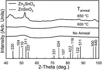
In Fig. 1, we show XRD data obtained from ZTO films before and after annealing to 600 and 650 °C. As shown, there is a lack of diffraction peaks in the spectra for both the as-deposited and 600 °C films, indicating that these films are amorphous.Reference Chiang, Wager, Hoffman, Jeong and Keszler3 These results are similar to those published previously for ZTO films where a broad peak at 56° is representative of amorphous ZTO.Reference Nomura, Ohta, Takagi, Kamiya, Hirano and Hosono1, Reference Cheong, Yoon, Shin and Hwang16, Reference Jeong, Jeong and Moon21, Reference Young, Moutinho, Yan and Coutts28–Reference Khorami, Keyanpour – Rad and Vaezi30 Also shown in Fig. 1 are the locations of major diffraction peaks for both spinel Zn2SnO4 (solid lines) and ilmenite ZnSnO3 (dashed lines).Reference Chiang, Wager, Hoffman, Jeong and Keszler3 After annealing the ZTO films to 650 °C, we found that the ZTO crystallized, which is indicated by the sharp XRD peaks in the topmost spectrum shown in Fig. 1. These results are similar to prior literature,Reference Chiang, Wager, Hoffman, Jeong and Keszler3, Reference Young, Moutinho, Yan and Coutts28, Reference Ko, Kim, Kim, Lee, Lee, Cheong and Kim31, Reference Jin, Shulai, Honglei and Lingyun32 where the broad peak at 52.33° corresponds to the (311) Zn2SnO4 diffraction plane. We found that spinel Zn2SnO4 was the dominant crystalline phase after annealing at 650 °C, which matches the results from several other authors and is expected based on the stoichiometry of the films.Reference Stambolova, Toneva, Blaskov, Radev, Tsvetanova, Vassilev and Peshev33–Reference Ivetić, Nikolić, Nikolić, Blagojević, Đurić, Srećković and Ristić35 Secondary electron microscopy (SEM) images of the as-deposited ZTO film were very smooth and did not show grain structure that would be consistent with crystallization. These results suggest that the as-deposited films are amorphous and are in agreement with the XRD results discussed above.
XRD spectra for as-deposited ZTO thin films and after annealing to 600 and 650 °C.

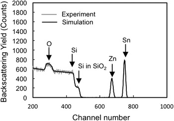
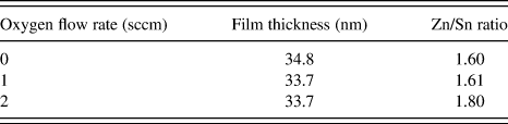
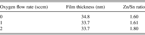
In Fig. 2, we show experimental and simulated RBS spectra for as-deposited ZTO films with 0 sccm of oxygen. The features are labeled in the spectra, where Zn and Sn are found at higher channel numbers, corresponding to higher energy, due to their higher atomic mass. Likewise, Si and O are at lower channel numbers, corresponding to lower energy, due to their lower atomic mass. The signals for Si are due to both the SiO2 layer and the Si substrate, while signals for O are due to both the ZTO and SiO2 layers. In the SIMNRA simulation, the sample is divided into several layers with varying thickness and composition. Experimental parameters such as incident ion energy, ion scattering angle, atomic number of incident ion, solid angle of detection, and energy calibration values for detectors were entered into the SIMNRA simulation software to calculate the backscattered spectra. The values of film composition and areal densities were varied to match the simulated and experimental spectra.Reference Mayer27 Based on this analysis, the as-deposited film had a slight depletion of Zn compared to the target composition as indicated in Table I. A depletion of Zn from sputter-deposited ZTO films, when compared to target composition, has been previously reported,Reference Satoh, Kakehi, Okamoto, Murakami, Uratani and Yotsuya12, Reference Minami, Takata, Sato and Sonohara36, Reference Minami, Sonohara, Takata and Sato37 where depletion values of ∼10% have been observed. A ∼30% zinc depletion has also been reported for sputter-deposited IGZO thin films, and it was proposed that the origin of this Zn depletion could result from the presence of multiphase polycrystalline grains in the sputter target and the lower deposition rate for ZnO compared to In2O3 and Ga2O3.Reference Oliziersky, Barquinha, Vilá, Magaña, Fortunato, Morante and Martins38 Similar effects may occur for the ZTO system as well where multiphase polycrystalline grains may exist in the sputter target and that ZnO has a lower deposition rate than SnO2. These results suggest that methods to fabricate sputter targets with uniform and reproducible composition and phase may be important for TAOS. The determination of the O atomic concentration from the RBS data is complicated by the relatively low intensity and the fact that the ZTO film was deposited on an oxidized substrate. The average molar ratio of Zn/Sn for the as-deposited ZTO films was 1.6 for 0 and 1 sccm O2 flow rates and 1.8 for 2 sccm O2 flow rates. These values give film stoichiometries of Zn1.6SnO3.6 and Zn1.8SnO3.8, respectively, where we used the ZnO and SnO2 stoichiometry to determine the value for oxygen in the film. The oxygen flow rate for each deposition condition is given in Table I, and we found that the Zn/Sn ratio increased for higher oxygen partial pressures. It is possible that the relative deposition rate of SnO2 is reduced relative to ZnO by the addition of oxygen resulting in the increased Zn/Sn ratio observed for depositions with 2 sccm of oxygen. The film thicknesses are reported in Table I, where the areal densities determined by RBS were converted to thickness using the reported density for crystalline Zn2SnO4,Reference Annamalai, Eo, Im and Lee39 although films may be slightly thicker since amorphous films are typically less dense than crystalline films of the same material.Reference Kamiya, Nomura and Hosono25
RBS spectra from an as-deposited ZTO film with 0 sccm of oxygen.

Thickness and Zn/Sn atomic ratios as determined by RBS.
We have used high-resolution XPS to investigate changes in chemical state and surface impurities on the ZTO films due to changes in deposition and postprocessing conditions. Since the films are insulating, we set the position of the main low energy C 1s peak (aliphatic carbon) to 284.6 eV to compensate for any charge-induced shifts in the following analysis. XPS survey spectra had peaks due to zinc, tin, oxygen, and carbon for the ZTO films. High-resolution spectra were obtained for the Zn 2p 3/2, Sn 3d 5/2, O 1s, and C 1s core levels. For these spectra, peak fitting was performed using XPSPEAK4.1.40 The procedure used for this analysis was consistent for all spectra from all the samples. A linear background was used for the peak fitting, where the number of peaks, the relative area, the full width at half maximum (FWHM), the %Lorentzian–Gaussian (%L–G), and the binding energy peak positions were adjusted. The sharpest and most intense photoelectron peaks from the ZTO were obtained for films annealed to 600 °C, and these data were used to define the initial fitting parameters. Similar procedures have proven successful to fit O 1s spectra where detailed information related to the adsorption of molecules on well-defined oxide surfaces can be obtained.Reference Herman, Dohnalek, Ruzycki and Diebold41 However, for the C 1s spectra, the room temperature films were used to obtain the fitting parameters due to the corresponding higher intensity due to the higher residual surface contamination.
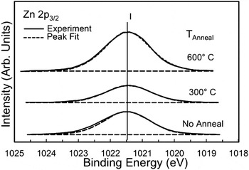
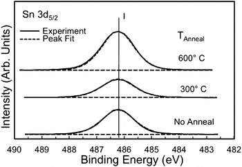
In Figs. 3 and 4, we show the Zn 2p 3/2 and Sn 3d 5/2 spectra for as-deposited films with 1 sccm of oxygen and films annealed to 300 and 600 °C. Based on the peak fitting analysis described above, we obtained FWHM and %L–G values of 1.65 and 1.38 eV, and 40% and 45%, respectively. As shown, a single peak with the indicated parameters was required to provide an adequate fit to all the Zn 2p 3/2 and Sn 3d 5/2 spectra. After charge compensation, the binding energies for Zn 2p 3/2 and Sn 3d 5/2 were determined to be 1021.49 and 486.22 eV, respectively, which are close to published values for ZnO and SnO2, characteristic of Zn2+ and Sn4+, respectively.Reference Kim, Kim, Ha, He, Kanatzidis, Facchetti and Marks11, Reference Seo, Hwang and Bae20 We also found that the Zn 2p 3/2, and Sn 3d 5/2 binding energies were nearly identical for films deposited with 0, 1, and 2 sccm of oxygen and irrespective of annealing conditions. Recent XPS results from ZTO films deposited by flash evaporation techniques suggest that the Zn 2p 3/2 and Sn 3d 5/2 require two or three components for adequate peak fitting, respectively, even after annealing the films up to 450 °C.Reference Jain, Kumar, Kumar, Jain, Bhandari and Vijay42 The data from this prior study may require these additional components due to a higher defect concentration for this deposition method as compared to RF sputter deposition.
XPS of Zn 2p 3/2 from ZTO films deposited with 1 sccm of oxygen and annealed to 300 and 600 °C.

XPS of Sn 3d 5/2 from ZTO films deposited with 1 sccm of oxygen and annealed to 300 and 600 °C.

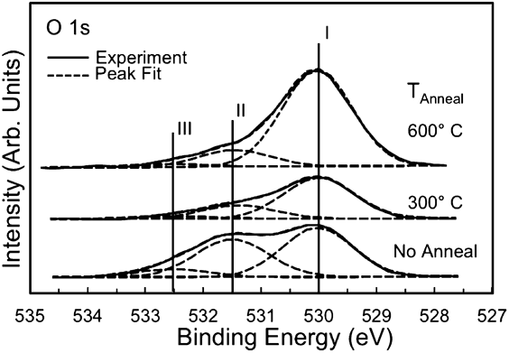
In Fig. 5, we show O 1s spectra for as-deposited ZTO films with 1 sccm of oxygen and films annealed to 300 and 600 °C. To obtain the O 1s peak fitting parameters, the 600 °C annealed films were used since the high-energy shoulder did not significantly influence the peak fitting parameters for the main feature in the spectrum. From this analysis, we obtained FWHM and %L–G values of 1.42 eV and 10%, respectively, for the main O 1s spectral feature. We used these fitting parameters to fit the O 1s spectra for all the samples. Our first pass through the analysis was to add a second O 1s peak for all the sample conditions to account for the higher binding energy features. For this analysis, we found that it was necessary to include a third peak, especially for the samples processed at lower temperatures. For the final analysis of the O 1s data, we fixed the positions of the higher energy peaks with respect to the main low binding energy feature for all the O 1s spectra for self-consistency. The three peaks were found to have binding energies of 530.02, 531.50, and 532.52 eV. We propose that the lower energy peak (I) at 530.02 eV corresponds to lattice oxygen ions, which have neighboring Zn and Sn ions. The higher energy peak (II) at 531.50 eV can be assigned to oxygen from a hydroxide species present on the surface and in the films. The highest energy peak (III) at 532.52 eV can be assigned to oxygen from water and carbonate present on the surface and in the film.Reference Kim, Kim, Ha, He, Kanatzidis, Facchetti and Marks11, Reference Seo, Hwang and Bae20, Reference Jeong, Ha, Moon, Facchetti and Marks43–Reference Deng, Verdaguer, Herranz, Weis, Bluhm and Salmeron46 The FWHM of the hydroxyl (II) and water/carbonate (III) peaks were allowed to have a slightly higher FWHM (1.47 eV) compared to the substrate peak. This is to account for any inhomogeneity in the chemical bonding for the hydroxyl and water/carbonate for the films, and this likewise improved the quality of the fit. We found that these higher energy peak intensities were significantly reduced after annealing the films and this is likely due to desorption of water and carbon oxides from the surface through the recombination of hydroxyl species or via molecular desorption.Reference Nomura, Kamiya, Ohta, Hirano and Hosono47
XPS of O 1s from ZTO films deposited with 1 sccm of oxygen and annealed to 300 and 600 °C.
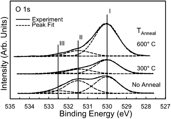
We have also performed in situ annealing experiments where the samples were heated to 550 °C for 15 min with an oxygen background pressure of 1 × 10⁻⁶ Torr. XPS was then performed without exposure to ambient atmosphere. We found that we were able to fit the O 1s spectra with a single peak using fitting parameters approximately the same as those defined above (i.e., no higher energy O 1s peaks). Since the anneal is at lower temperature than the 600 °C ambient anneal and under an oxygen-deficient atmosphere, we believe that these results confirm that the higher energy peaks are due to impurities that can desorb from the films during the annealing process. Likewise, we propose that the higher energy peak at 531.50 eV is due to hydroxyl contamination at the surface even for the samples annealed at 600 °C in ambient.
Other studies have also fit three components for the O 1s peak for ZTO and related materials.Reference Kim, Kim, Ha, He, Kanatzidis, Facchetti and Marks11, Reference Seo, Hwang and Bae20, Reference Jain, Kumar, Kumar, Jain, Bhandari and Vijay42, Reference Jeong, Ha, Moon, Facchetti and Marks43 Our peak assignments are somewhat different from several of these prior studies where it has been suggested that peak I corresponds to lattice oxygen ions, which have neighboring Zn and Sn ions (same as our assignment). The higher energy peak (II) corresponds to lattice oxygen in oxygen-deficient regions (different than our assignment). The highest energy peak (III) corresponds to a hydroxide species (different than our assignment). If the higher energy peak (II) is due to lattice oxygen in oxygen-deficient regions, one would expect that the relative intensity for this feature would increase for our in situ annealing experiments. However, this feature was completely eliminated in the O 1s spectra after the in situ anneal suggesting that this component is due to a species that desorbs from the film upon annealing. Recent O 1s XPS results for indium oxide films formed by combustion synthesis are consistent with our peak assignments.Reference Kim, Kanatzidis, Facchetti and Marks48 More detailed studies still need to be performed on model systems to better understand the assignment of these species and their role on device characteristics.
It has recently been observed that TFTs fabricated with sputter-deposited ZTO had much improved stability when the films were deposited at elevated temperatures compared to films that were postannealed to the same temperature ex situ.Reference Fakhri, Görrn, Weimann, Hinze and Riedl49 In this study, it was found that a lower density of states was present in the subband gap region for the in situ annealed samples. These subband gap states can provide electron traps that can influence the stability of the devices or modify their interaction with adsorbates. Based on our XPS measurements, there is likely to be significant impurities remaining on the back channel of devices annealed in ambient conditions. This suggests that annealing in vacuum may be a necessary step to improve device stability due to contamination of the ZTO film. These surface species may significantly alter the contact of metal layers on ZTO as well.Reference Choi50
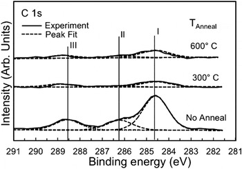
In Fig. 6, we show C 1s spectra for as-deposited ZTO films with 1 sccm of oxygen and films annealed to 300 and 600 °C. The C 1s spectra had three fairly well-separated peaks, where all three were reduced in intensity after annealing the films. To obtain peak fitting parameters for the C 1s peak, we used the low energy peak from the unannealed films due to the higher residual concentration of adventitious carbon on the surface. The FWHM and %L–G were determined to be 1.32 eV and 40%, respectively. Peak fitting of C 1s spectra allowed us to determine binding energies for three peaks, with the lower energy peak having an energy of 284.6 eV (I), which is assigned to aliphatic carbon (C–C or C–H bonds), and the two higher energy peaks at 286.21 eV (II) and 288.57 eV (III) can be assigned to C–O and C = O groups on the surface, respectively.Reference Deng, Verdaguer, Herranz, Weis, Bluhm and Salmeron46, Reference Xie, Zhao, Chen, Zhao and Yuan51 Finally, using these fitting procedures, we have found that the binding energies for Zn 2p 3/2, Sn 3d 5/2, O 1s, and C 1s core levels from all the analyzed samples were very consistent and varied <0.1 eV.
XPS of C 1s from ZTO films as-deposited with 1 sccm of oxygen and annealed to 300 and 600 °C.

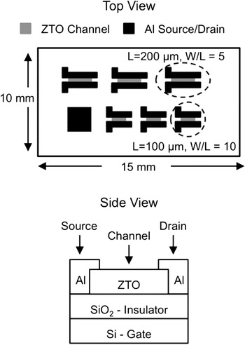
In Fig. 7, we show a schematic of the TFT test structures that have been used to characterize the electrical performance of the ZTO films. The upper portion of the figure shows the top view of the devices, including the dimensions, while the lower portion of the figure shows the side view of the devices. For these studies, we have patterned the ZTO channel to minimize errors in extracting electron mobilities due to fringe currents outside the channel region.
Schematic of TFT test structure.

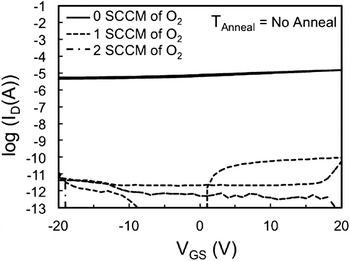
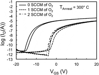
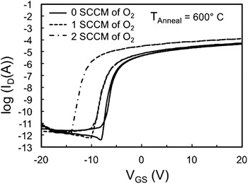
In Figs. 8–10, we show the transfer characteristics for ZTO TFTs that have not been annealed or have been annealed to 300 or 600 °C, respectively. For these measurements, the drain current (I D) and gate current (I G) were measured, while the gate to source voltage (V GS) was scanned from −20 to 20 V in a double sweep mode where the drain to source voltage (V DS) was held constant at 1 V. In this work, we use the definition of the turn-on voltage (V on), which is the gate voltage at which there is sharp increase in I D in the log (I D) − V GS transfer curves.Reference Hoffman52 Other parameters of interest include the I D, on-to-off ratio (I on/I off), threshold voltage (V th), subthreshold slope (S), and channel mobility (μavg).
TFT transfer characteristics with as-deposited ZTO channel layer with 0, 1, 2 sccm of oxygen.

TFT transfer characteristics with ZTO channel layer deposited with 0, 1, 2 sccm of oxygen and annealed to 300 °C.

TFT transfer characteristics with ZTO channel layer deposited with 0, 1, 2 sccm of oxygen and annealed to 600 °C.

The value of average channel mobility was extracted using,

where G CH is the value of channel conductance with respect to V GS, W/L is the width to length ratio of the channel, and C ins the capacitance of the SiO2 insulator.Reference Hoffman52
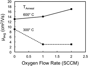
As shown in Fig. 8, the as-deposited ZTO TFTs do not have typical transistor characteristics. We found that the ZTO films deposited with 0 sccm of oxygen were conducting, which is evident from the high drain current with no modulation of I D with V GS, whereas when oxygen was added during deposition, the films became insulating, which is evident from the low drain currents. After annealing the ZTO to 300 and 600 °C, we have found that the TFTs have negative V on of approximately −15 to −5 V depending on chamber oxygen flow rates and annealing conditions. This suggests that carrier concentration can be controlled by the O2 partial pressure during deposition where higher carrier concentration shifts the turn-on voltage more negative. Hong et al.Reference Hong, Chiang and Wager6 observed similar results for sputter-deposited ZTO TFTs. Another important parameter that determines the switching quality of TFTs is the I on/I off.Reference Chang, Lee, Herman and Chang8 Both Figs. 9 and 10 show that the I on/I off can be greater than 106 for a broad range of processing conditions and their value increased with increasing anneal temperature. Channel mobility is another parameter that quantifies the performance of the semiconductor channel.Reference Chiang, Wager, Hoffman, Jeong and Keszler3 The average mobility (μavg) corresponds to the average mobility of all carriers in the semiconductor channel. We have found that the average mobility for a given oxygen flow rate increases with increase in temperature due to a variety of reasons, including the modification of the semiconductor–insulator interface and the change in the nature of traps in the semiconductor.Reference Chiang, Wager, Hoffman, Jeong and Keszler3, Reference Hoffman4 It was observed that the average channel mobility changed with respect to oxygen flow rate with two different trends. As shown in Fig. 11Reference Hong, Chiang and Wager, the ZTO samples annealed at 300 °C had a significant decrease in μavg with increasing oxygen flow rate, while at 600 °C, there was a slight increase in μavg with increasing oxygen flow rate. These results indicate that the ZTO films electrical properties are still strongly influenced by the film deposition conditions for lower annealing temperatures, while the initial deposition conditions are less important for higher annealing temperatures.Reference Hoffman52 Very good device performance was obtained for ZTO TFTs sputter deposited with 2 sccm of oxygen and annealed to 600 °C where the following parameters were determined: μavg = 17 cm2/Vs, V th = −1.5 V, S = 0.9 V/decade, V on = −12 V, and I on/I off > 107. After a 600 °C anneal, we found that the TFTs do not have significant hysteresis between the sweep up and down traces, suggesting that if traps are present, they have the ability to stay in equilibrium with the sweep rate of the gate voltage. The hysteresis observed for the 300 °C annealed devices may be due to states related to an oxygen deficiency in the ZTO film, which may enhance the adsorption, reaction, and diffusion of adsorbates into the film.
Change in average channel mobility as a function of oxygen flow rate and postannealing conditions.

We have found that annealing the ZTO films resulted in significant changes in the device characteristics and the relative concentration of oxygen impurities on the surface of the ZTO films. In general, the electrical properties of the films can be modified by both the deposition conditions and annealing temperature, where insulating, semiconducting, or conducting ZTO can be obtained. High average mobilities were obtained for ZTO TFTs suggesting that this material can be considered a replacement for amorphous silicon TFTs for next generation displays. Control of the surface chemistry of the ZTO films may help to improve both device stability and the formation of interfacial layers for source/drain contacts.
IV. CONCLUSIONS
We have analyzed the role of both deposition and postannealing conditions on ZTO film structure, composition, surface contamination, and TFT device performance. We found that the ZTO thin films were amorphous even after annealing to 600 °C and that the as-deposited ZTO film composition was close to the target stoichiometry of Zn2SnO4. XPS indicated that the ZTO films had significant surface contamination. Upon annealing in ambient, we found that the surface contamination was significantly reduced; however, it was necessary to anneal under vacuum to remove all the oxygen containing impurities. ZTO TFTs with very good electrical performance were obtained where the following parameters were obtained for a device annealed to 600 °C: μavg = 17 cm2/Vs, V th = −1.5 V, S = 0.9 V/decade, V on = −12 V, and I on/I off > 107. Device results indicate that the electronic properties are closely linked to deposition conditions, surface contamination, and postprocessing conditions. Finally, we propose that the three components observed in the O 1s spectra are due to lattice oxygen ions, which have neighboring Zn and Sn ions, oxygen from a hydroxide species present on the surface and in the films, and oxygen from water and carbonate present on the surface and in the film.
ACKNOWLEDGMENTS
This research was performed in part using facilities at the Microproducts Breakthrough Institute and the Materials Synthesis and Characterization Facility at Oregon State University and at the Environmental Molecular Sciences Laboratory, a national scientific user facility sponsored by the U.S. Department of Energy’s Office of Biological and Environmental Research located at Pacific Northwest National Laboratory (PNNL). J.S.R. thanks PNNL for providing an Alternate Sponsored Fellowship during a portion of these studies. The project was funded by the Oregon Nanoscience and Microtechnologies Institute and the Office of Naval Research under contract number 200CAR262.