Introduction
Increasing data rates in mobile wireless communication systems require antenna array systems with a large number of active antenna elements and advanced beamforming capabilities, and one of the challenges in achieving this is a high degree of integration between the radiating elements and the active devices in order to minimize the size and cost of massive multiple-input and multiple-output (MIMO) arrays. In [Reference Khoshniat, Yekan, Baktur and Warnick1–Reference Lu4], the antennas combined with power amplifiers (PAs) on printed circuit boards were designed to improve the power efficiency and radiated power in sub-6G bands. However, as the frequency increases, the power loss of the matching networks and harmonic suppression networks introduced between the PAs and antennas significantly increases [Reference Vilenskiy5, Reference Hasegawa and Shinohara6].
The millimeter-wave antennas have much smaller size than the sub-6 GHz antennas, making it possible to be designed on the chip package. Antenna-in-package (AiP) is one of feasible solutions for millimeter-wave devices to achieve miniaturization, high integration, and excellent performance [Reference Zhang and Liu7, Reference Zhang and Mao8]. Several manufacturing technologies and substrates are used for the AiP designs, including low temperature co-fired ceramic (LTCC) [Reference Zhu, Yang, Li, Liao and Xue9, Reference Chou, Chou and Deng10], high-density interconnect (HDI) [Reference Wang, Shi, Xu and Yin11–Reference Xia13], embedded wafer level ball grid array (eWLB) [Reference Frank14, Reference Fischer, Tong, Hamidipour, Maurer and Stelzer15], organic substrate [Reference Xue, Wan, Wang and Cao16], glass [Reference Lin17, Reference Galler, Frey, Waldschmidt and Chaloun18], and ceramic [Reference Song19]. For example, a 60 GHz single-ended-fed planar aperture antenna using LTCC process was designed for AiP applications [Reference Zhu, Yang, Li, Liao and Xue9]. In the design, an open cavity was employed in the LTCC package to enhance the antenna gain. The peak gain reaches 11.5 dBi for the antenna and 20.4 dBi for the array. In [Reference Chou, Chou and Deng10], an AiP design with LTCC technology for W-band applications has been proposed, presenting a new solution for the special case where metal package with high mechanical strength is needed. The prototype achieves a −10 dB impedance bandwidth of 10 GHz from 88 to 98 GHz and a peak gain of 12.3 dBi at 89 GHz. However, the high cost of the LTCC process has limited its large-scale applications. Thus, technologies such as HDI and fan-out wafer level packaging (FOWLP) are developed for low-cost production of millimeter-wave AiPs. An organic multi-layer industry standard HDI process was used to achieve a high-performance, cost-effective AiP module [Reference Xia13]. For both polarizations, the proposed antenna element has a fractional impedance bandwidth of 23.1%, and their peak gain is above 5.45 dBi. A directional folded dipole antenna was designed in an embedded eWLB array package in [Reference Fischer, Tong, Hamidipour, Maurer and Stelzer15]. Nevertheless, parasitic effects from the interconnections between the antenna and millimeter-wave circuit dies in the package will lead to degradation of the matching performance.
In this work, a compact active integrated antenna based on a highly compatible AiP solution is proposed. It is composed of a cover plate integrated with a patch antenna and a package backplane carrying a GaN PA die. The AiP solution provides efficient interconnection between the antenna and the GaN PA die while providing physical shielding. Moreover, it can improve the impedance matching performance of the PA die and offset the parasitic effects in the package. A cavity located within the cover plate is cut by laser to accommodate the die. The package backplane integrates plated through holes (PTHs) to provide DC bias and RF signal for the die, as well as a PTH array to improve heat dissipation. The AiP solution is compatible with RFIC dies with different pin arrangements. The design of the active integrated antenna based on the AiP solution is detailed in second section, along with the simulation results and the thermodynamic analyses. The active integrated antenna is implemented and the experimental results are shown in next section. In addition, the AiP solution is also applied to a GaN front-end module (FEM) die to verify its compatibility. Finally, a conclusion is given in last section.
Active integrated antenna design
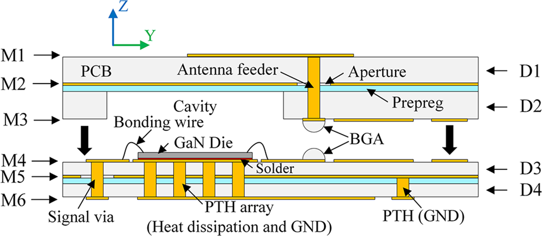
The compact active integrated antenna based on a highly compatible AiP solution is illustrated in Fig. 1. It consists of a cover plate (substrate D1–D2, layer M1–M3), a package backplane (substrate D3–D4, layer M4–M6), and a GaN PA die integrated in between. The GaN PA die is mounted on the package backplane with bonding wires. And then the cover plate integrated with an antenna is bonded to the package backplane using the conductive adhesive for compactness. Moreover, the antenna on the cover plate provides impedance compensation for the GaN PA die, improving impedance matching performance.
Configuration of the proposed active integrated antenna.

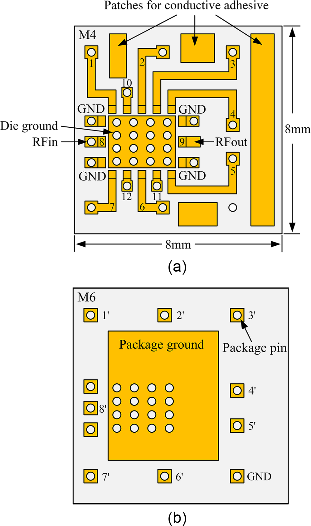
The GaN PA die employs a two-stage common source structure, unconditional stability technique and matching networks combining both low-pass and high-pass filters to achieve more than 1 W of saturated output power in the 24–30 GHz frequency band. The GaN PA die is connected to its surrounding pins on the package backplane by using bonding wires. Figure 2 shows the circuit layout on the layers M4 and M6 of the AiP design, the top and bottom layers of the package backplane. The pin 9 for the output port of the die is expected to be connected to the cover plate with the antenna, while the pins 1–8 are extended through the PTHs to M6, serving as the external interfaces for the active integrated antenna. Note that each PTH is equipped with an aperture with a larger diameter etched in the GND on M5 to avoid the PTH being short-circuited. In addition, three grounding pins 10–12 on M4 are connected to the GND on M5 through the PTHs. The back of the die is soldered to a grounding plane in the middle of M4, and a PTH array routed from M4 to M6 is designed to connect this grounding plane with the GND on M5 and a large copper sheet on M6, which greatly improves the heat dissipation performance. Moreover, all the PTHs are filled with resin not only to avoid the solder paste being sucked into the PTHs during the assembly process of the AiP design, but also to further enhance heat dissipation. In order to guarantee the shielding performance of the package and the reliability of the bond between the package backplane and the cover plate, four specific patches are designed on both M3 and M4.
Layout of the circuits on (a) M4 and (b) M6.

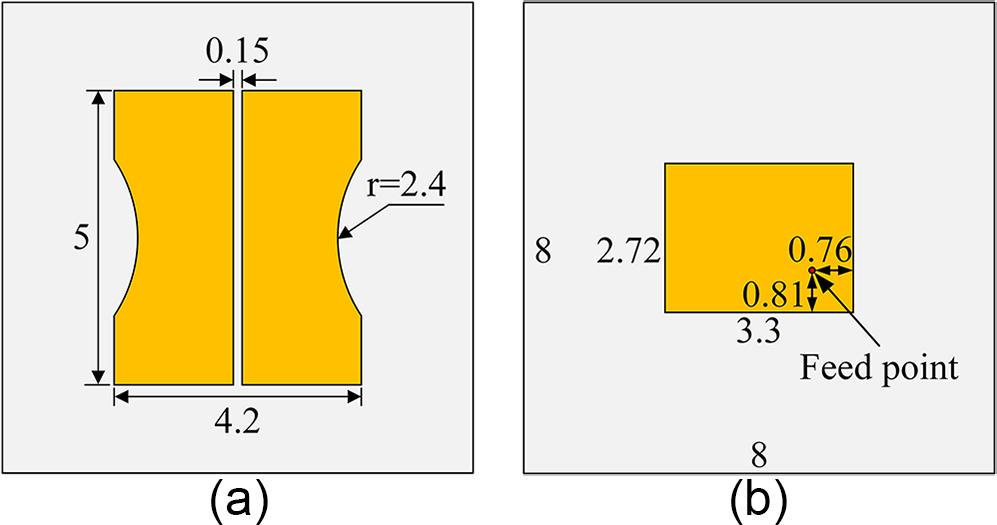
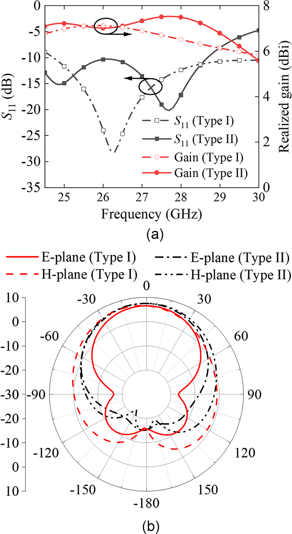
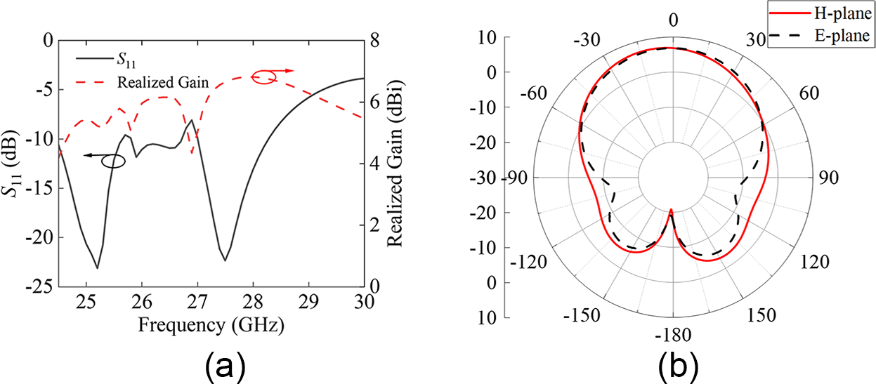
In the cover plate, the antenna is located on layer M1, and its feeding structure is routed from M1 to M3 as shown in Fig. 1. The metal on M2 not only serves as the GND of the antenna, but also isolates the antenna from the GaN PA die to avoid electromagnetic interference. A cavity is cut by laser in D2 to accommodate the GaN PA die mounted on the package backplane. Figure 3 shows two types of millimeter-wave wideband patch antennas that can be designed on M1. The type I antenna employs a coupled-feed, curved edges and rectangular slot structures to introduce additional current paths for wideband radiation. In contrast, the type II antenna uses a coaxial feed with the feed point set near the diagonal of the radiator. It consequently excites two operating modes with similar resonant frequencies along the two adjacent edges of the radiating patch, which improves the frequency bandwidth. It is worth noting that the input impedance of the Type II antenna varies with the position of the feed point, which creates conditions for direct connection of the antenna to the PA die. Both antennas with different feeding methods are suitable for the proposed AiP solution. Figure 4 shows the return loss, realized gain, and radiation pattern of the antennas on the cover of the package. As seen, the return loss of the type I antenna is better than −10 dB in the frequency band of 24.7–28.8 GHz with a peak gain of about 7 dBi, while the type II antenna works in the frequency band of 24.2–28.7 GHz with a peak gain of 7.5 dBi. In this work, the type II antenna with smaller size, wider frequency bandwidth and flat gain is chosen in the following design.
Layout of the radiator on M1 (unit: mm): (a) Type I; (b) Type II.

Simulation results of the patch antennas on the cover of the package: (a) S11 and the realized gain; (b) radiation pattern at 28 GHz.

The GaN PA die is measured on a probe station to obtain its port impedance, and the input impedance of the antenna is subsequently adjusted to the conjugate of the output impedance of the GaN PA die to achieve a low-loss direct connection between them. Finally, the cover plate and package backplane are bonded by conductive adhesive. The RF signal is input to the active integrated antenna via the pin 8′ on the package backplane, which is transmitted to the GaN PA die, and then fed to the antenna on the cover plate via the pin 9 for radiation. The AiP solution is compatible with a variety of RFICs with different pin arrangements. In the proposed design, the substrate of Rogers 3003 with the dielectric constant of 3.0 and loss tangent of 0.001 is adopted. The whole package includes four layers of PCB substrates, the thickness of which from D1 to D4 are 0.508, 0.508, 0.254, and 0.254 mm, respectively. The adjacent substrates are bonded by a layer of prepreg with the thickness of 0.1 mm. The type of the prepreg is 3313, which is commonly used in PCB processing. The copper thickness is 0.018 mm. The overall dimensions of the proposed active integrated antenna are 8 mm × 8 mm × 1.7 mm. In order to evaluate the performance of the package, the whole passive AiP design is simulated. Figure 5 shows the return loss, realized gain, and radiation pattern of the passive AiP design. As observed, the AiP design still works in the frequency band of 24.4–28.3 GHz. Compared with the antenna on the cover simulated in Fig. 4, the diameter of the PTHs in the AiP design has to increase from 0.1 mm to 0.3 mm to meet the machining accuracy requirement, resulting in slight performance degradation.
Simulation results of the passive AiP design: (a) S11 and the realized gain; (b) the radiation pattern at 28 GHz.

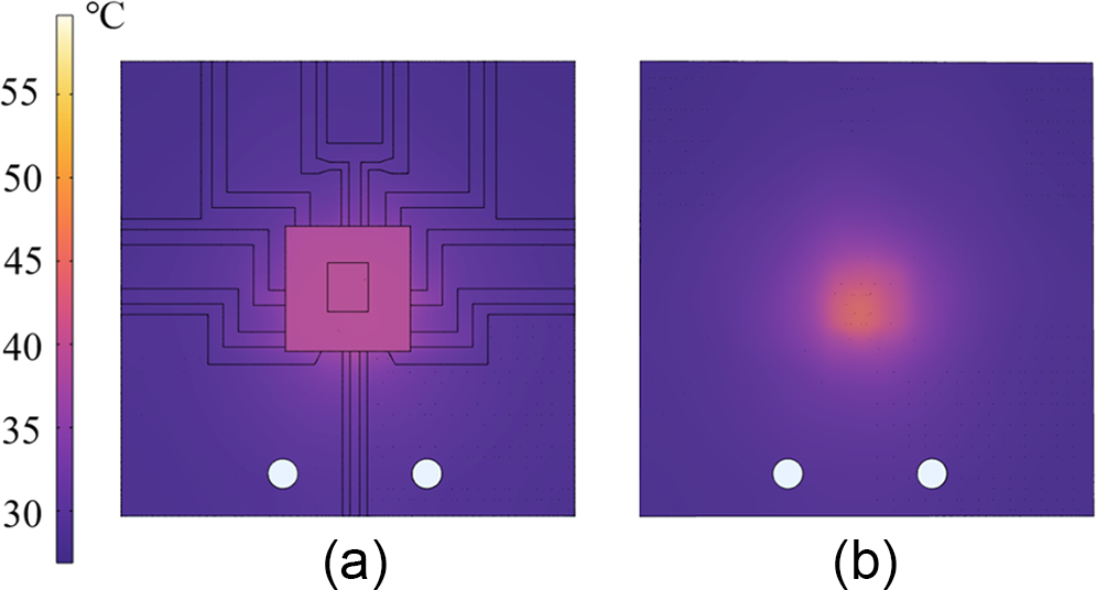
To demonstrate the heat-dissipating capability of the AiP design, a heat source with the thermal energy of 1W is placed on the grounding plane on the package backplane (M4) to simulate the heat generated by the GaN PA die when it operates. The package module is mounted on a test board using Rogers 3003 substrate with a size of 30 × 30 × 0.254 mm. The thermal conductivity (TC) of all materials is listed in Table 1. The ambient temperature is 25 ∘C. The simulated thermal performance is shown in Fig. 6, the maximum temperature of the AiP design is only 58 ∘C. As observed, the temperature distribution results show that the thermal radiation generated by the heat source can be effectively and uniformly conducted outside the package. Therefore, the proposed AiP design has excellent heat dissipation.
Simulated temperature distribution: (a) top view and (b) bottom view.

TC of the materials (unit: W/(M  $\cdot^{\ \circ}$C))

Experiment
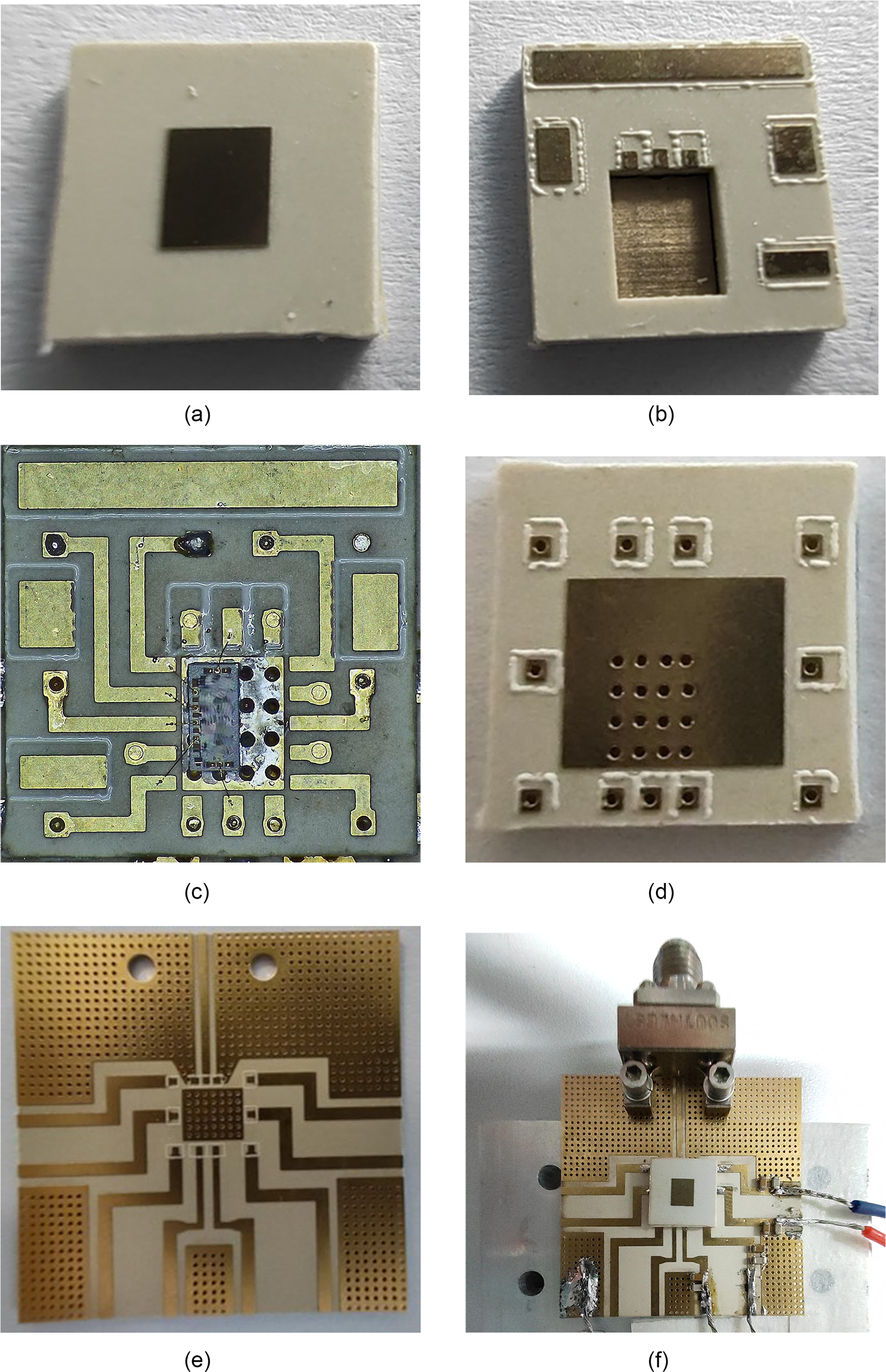
A test prototype of the proposed active integrated antenna is fabricated and measured. Figure 7 shows the top view and bottom view of the cover plate with the antenna and the package backplane with the GaN PA die, as well as a test board and the complete active integrated antenna prototype based on the AiP solution on the test board. First, the PA die is connected to the package backplane by a wire bonding process, while the back of the die is welded to the grounding plane with a PTH array below for heat dissipation, as shown in Fig. 7(c). The length of the bonding wires is limited to around 400 µm. Subsequently, the conductive adhesive is used to bond the cover plate with an antenna with impedance-compensated characteristics and the package backplane. Finally, the whole chip is welded to a test board for measurement, as shown in Fig. 7(f). The test board includes several pins to provide DC bias voltages and a 50 Ω transmission line for the input signal.
Photograph of the active integrated antenna: (a, c) top view and (b, d) bottom view of the cover plate and package backplane; (e) test board; (f) assembled prototype.

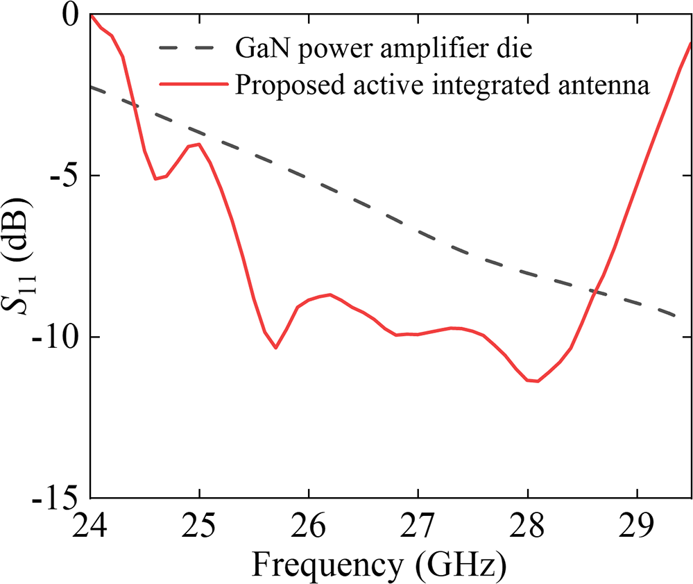
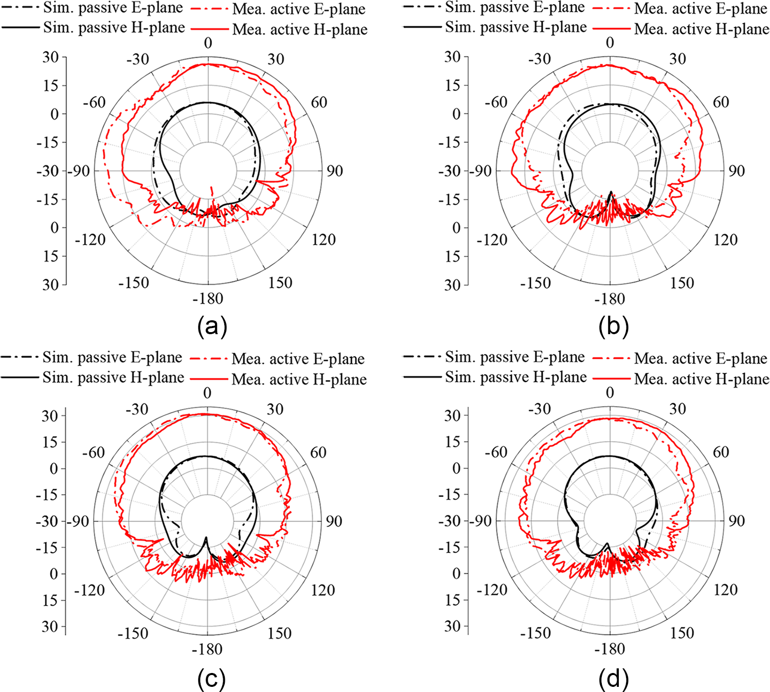
The measurements are conducted by using a vector network analyzer and an in-house far-field mm-wave measurement system [Reference Amadjikpe, Choudhury and Patterson21]. Figure 8 shows the return loss of the GaN PA die before assembly and the complete active integrated antenna based on the AiP solution. As seen, the S 11 is improved in the working frequency band of 25.7–28.7 GHz after the die is assembled into the package. Thus, the impedance matching performance degraded by the die processing error and parasitic effect can be improved by the proposed AiP solution. The far-field E-plane and H-plane radiation patterns of the active integrated antenna are presented in Fig. 9. As observed, the proposed active integrated antenna achieves a peak gain of 31 dBi.
Measured S 11 of the GaN PA die and the proposed active integrated antenna.

Radiation pattern of the proposed active integrated antenna: (a) 26 GHz; (b) 27 GHz; (c) 28 GHz; (d) 28.7 GHz.

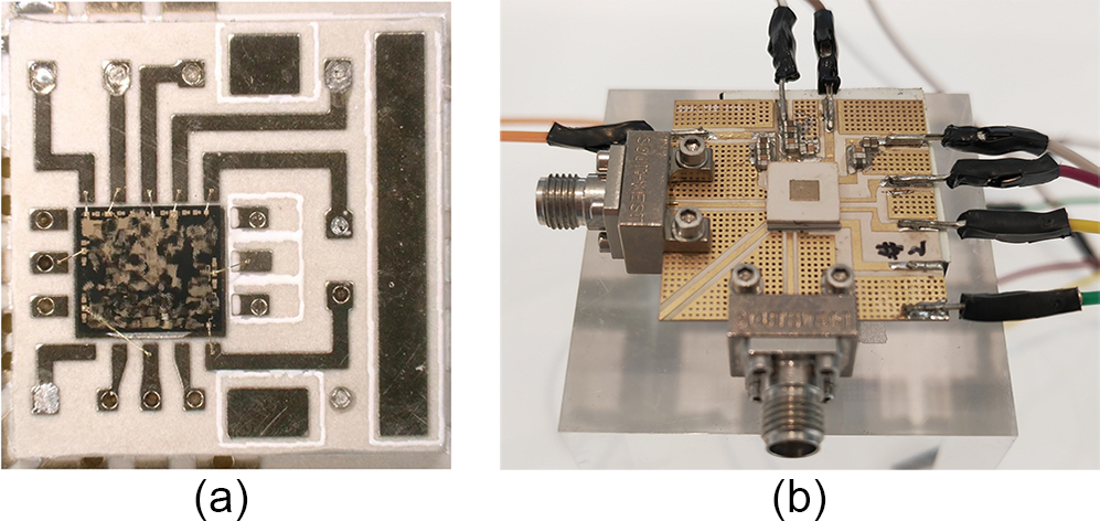
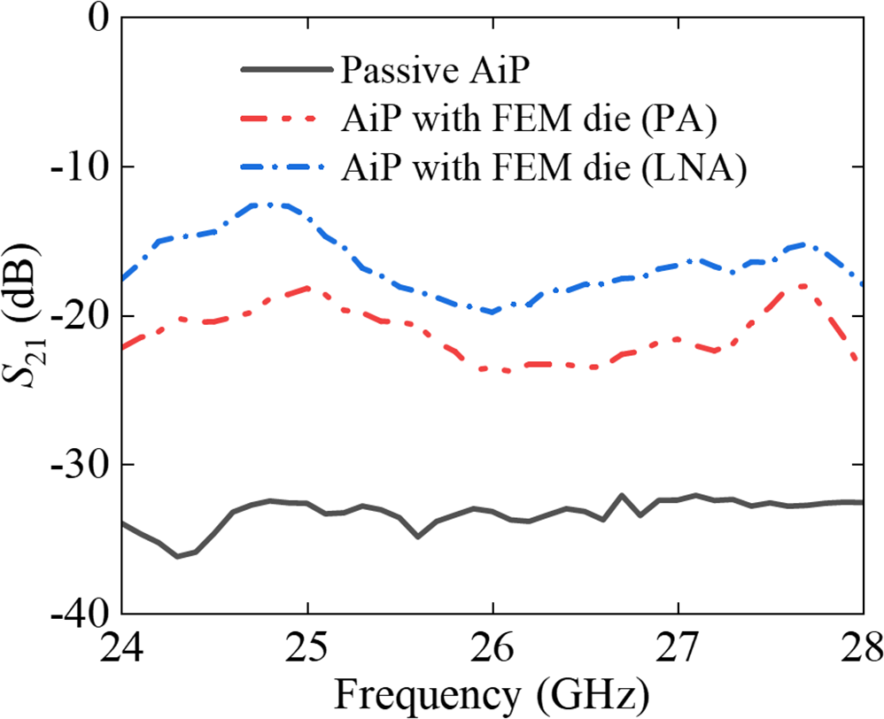
In order to verify the compatibility of the proposed AiP solution, another active integrated antenna based on a millimeter-wave GaN FEM die is designed. To be specific, a GaN FEM die working in the frequency band of 24.5–27.5 GHz is designed, fabricated and packaged by using the proposed AIP solution. The pin 6 (I/O port) and the extended grounding pins 11 and 12 on the package backage are used as the interface for the second RF signal channel of the FEM die. Figure 10(a) shows the FEM die mounted on the package backplane, and the assembled prototype is shown in Fig. 10(b). A standard horn antenna is adopted as the reference antenna to measure the transmission coefficient S 21 in the far-field region. Figure 11 shows the S 21 of the AiP design with and without the FEM die. It indicates that the proposed AiP solution is well adapted to the FEM die.
Photograph of (a) the GaN FEM die mounted on the package backplane and (b) the assembled prototype on the test board.

Measured S 21 of the AiP design with and without the GaN FEM die.

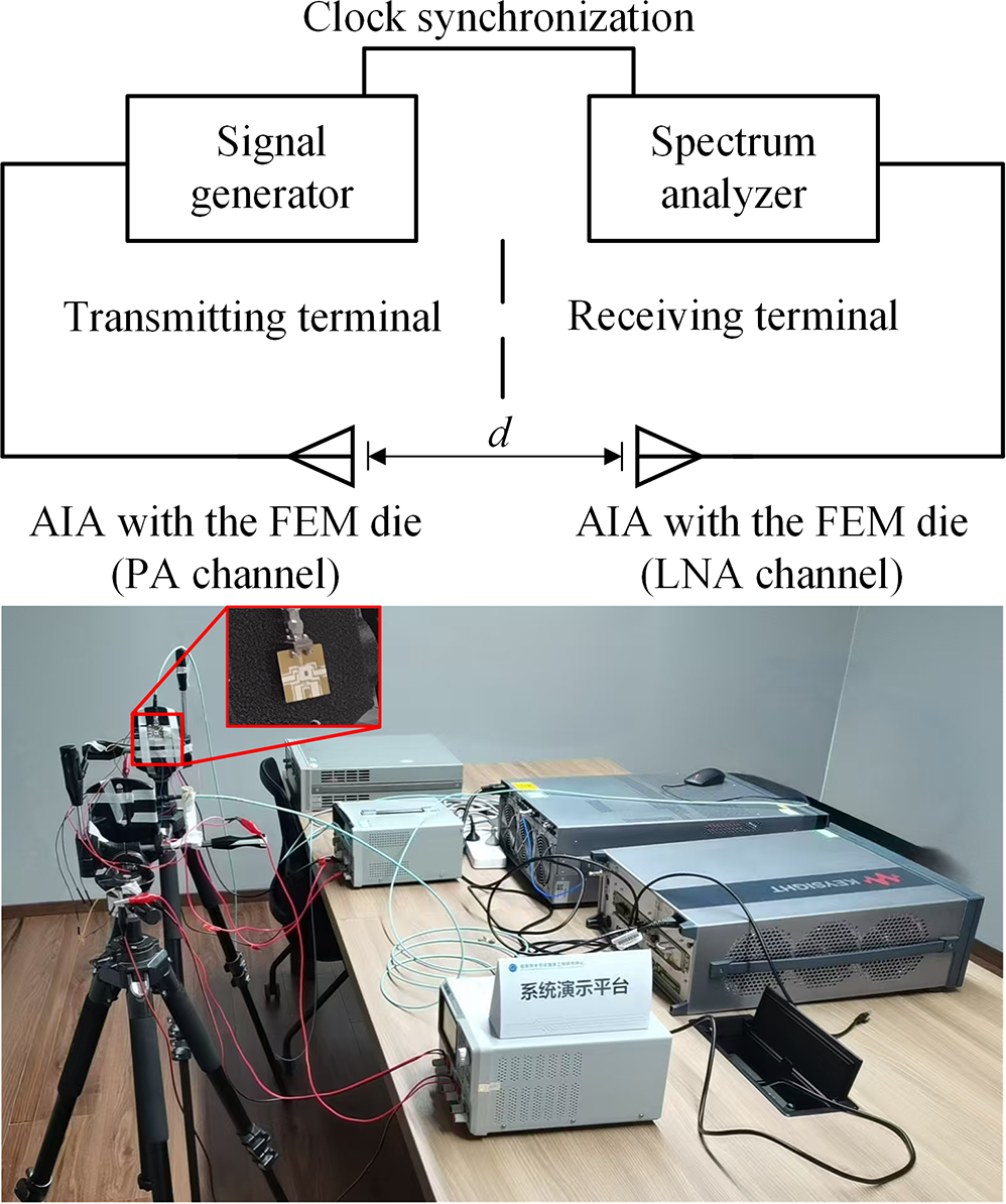
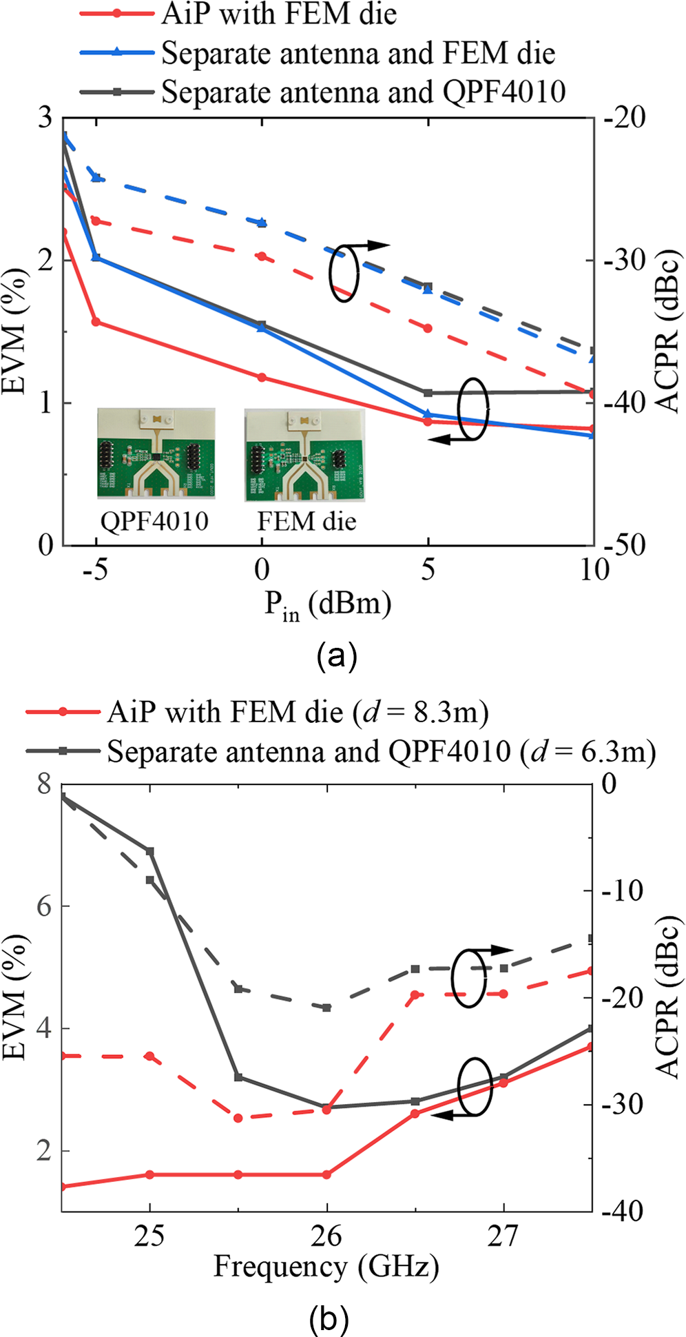
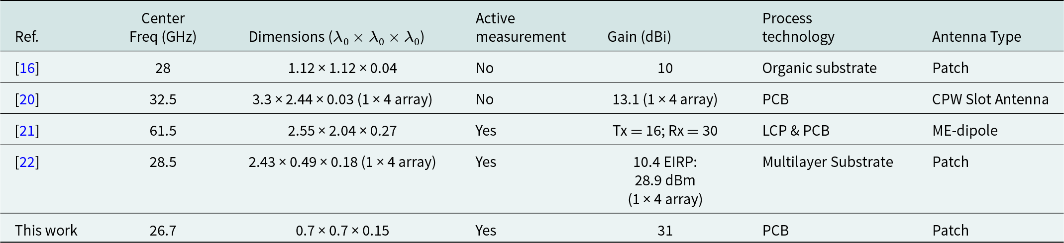
In addition, the error vector magnitude (EVM) and adjacent channel power ratio (ACPR) of the active integrated antenna with the FEM die are measured. To further evaluate the communication performance of the proposed active integrated antenna based on the highly compatible AiP solution, an active integrated antenna consisting of a separate antenna and the FEM die and an active integrated antenna consisting of a separate antenna and the commercial FEM (QPF 4010 from Qorvo) are also fabricated and measured for comparison. Note that the QPF4010 covers exactly the 24.5–27.5 GHz frequency range. The measurement setup is shown in Fig. 12. The measurement system consists of a signal generator with signal modulation function and a spectrum analyzer with signal demodulation function. In each measurement, two identical active integrated antennas are used as the transmitter and receiver, respectively. The experiments are conducted under atmospheric conditions at room temperature. The measured EVM and ACPR at 26 GHz are shown in Fig. 13(a). The distance d between the transmitter and receiver is 2 m to satisfy the far-field measurement condition. It can be seen that the active integrated antenna based on the proposed AiP solution has smaller EVM, ACPR and system size than the other two. Moreover, Fig. 13(b) demonstrates the EVM and ACPR of the active integrated antennas with the same input power. It can be seen that the proposed active integrated antenna based on the AiP solution still has better EVM and ACPR over longer distance. Finally, performance comparisons among the proposed active integrated antenna and some reported designs are listed in Table 2. It can be seen that the proposed active integrated antenna achieves the effect of high gain with a lower cost multi-layer PCB process while maintaining a compact size.
Measurement setup for the active integrated antennas (AIAs).

Measured EVM and ACPR of the three active integrated antennas versus (a) input power and (b) frequency.

Comparison among the proposed work and previous related works

Conclusion
A compact active integrated antenna covering 25.7–28.7 GHz has been proposed based on a highly compatible AiP solution. The AiP solution provides efficient interconnection and impedance compensation for the GaN PA die to improve the matching performance of the active integrated antenna. Moreover, it is highly compatible with RFIC dies with different pin arrangements. Based on this AiP solution, the active integrated antenna has the advantages of small size, high integration, good heat dissipation, easy fabrication and low cost. All of these make it one of the promising candidates for large-scale antenna array in millimeter-wave communication.
Acknowledgements
This work was supported in part by the National Natural Science Foundation of China under Grant 62101139, in part by the Guangdong Basic and Applied Basic Research Foundation under Grant 2023A1515012831, and in part by the State Key Laboratory of Millimeter Waves under Grant K202416.
Competing interests
None declared.

Zhi-Xia Du received the B.S. degree in applied physics and Ph.D. degree in information and communication engineering from South China University of Technology, Guangzhou, China, in 2014 and 2019, respectively.
From 2017 to 2018, he was with the Applied Electromagnetics Research Group, University of California, San Diego, CA, USA, as a Visiting Graduate. From 2019 to 2020, he worked as a senior engineer in Huawei Technologies Co., LTD., Shenzhen, China. He is currently an Assistant Professor with the School of Integrated Circuits, Guangdong University of Technology. He currently has more than 40 publications and more than 20 issued patents. His research interests include active antenna array, wireless power transfer, time-modulated metasurfaces and microwave circuits.
Dr. Du has served as Technical Program Committee (TPC) member and Session Organizer/Chair for a number of conferences. He was awarded the Best Student Paper Prize in the 2015 National Conference on Microwave and Millimeter Wave Technology (NCMMW).

Zhenming Pan received the B.S. degree in electrical engineering and automation from Guangdong Ocean University, Zhanjiang, China in 2022. He is currently pursuing the M.S. degree with the School of Information Engineering, Guangdong University of Technology, Guangzhou. His research interests include filtering antenna and high-efficiency antenna in package design for RF/microwave and millimeter-wave applications.

Jianqiang Chen received the B.S. degree in integrated circuit design and integrated system from Guangdong University of Technology, Guangzhou, China, in 2020, where he is currently pursuing Ph.D. degree. His research interests include broadband high-efficiency power amplifier design for RF/microwave and millimeter-wave applications.

Bo Sun graduated with his PhD degree from Delft University. His research focus is concerned with advanced RF/analog chip packaging and reliability. Currently he serves as the IEEE EPS Guangzhou Chapter Secretary and ICEPT RF Packaging Committee member.

Zhihao Zhang received the B.S. degree in Information Engineering, and the Ph.D., degree in Information Acquisition and Control from Guangdong University of Technology (GDUT), Guangzhou, China, in 2012 and 2017, respectively. During 2015–2017, he was studying in the Department of Electrical Engineering and Computer Science, University of California, Irvine as a visiting Ph.D. student. He currently serves as an Assistant Professor within the School of Integrated Circuits at GDUT. His research interests are focused on radio frequency circuit design, as well as information acquisition and control. He scholarly contributions include over 50 publications and more than 20 patents authorized or pending.

Chunbing Guo received the B.S. and M.S. degrees in information engineering from Southeast University, Nanjing, China, in 1994 and 1997 respectively, and Ph.D. degree in RFIC from The Hong Kong University of Science and Technology, Hong Kong, in 2001.
From 2002 to 2018, he was with IC companies designing mixed-signal IPs such as SerDes and GEPHY. He is currently a full professor with the School of Integrated Circuits, Guangdong University of Technology, Guangzhou, China. His research interests are focused on mixed-signal ICs such as ADC/DAC and high performance PLLs.