Introduction
In this lecture, I will describe research focused on semiconductor nanowires, although the time constraints will restrict this discussion to several key concepts and areas that we are pursuing at present. After providing a brief introduction to the types of nanomaterials that can serve as platforms for studying both fundamental science and advancing technology, I will focus on two basic areas of research. The first describes our ability to control the synthesis of semiconductor nanowiresReference Lieber, Morales, Sheehan, Wong and Yang1–Reference Jiang, Tian, Xiang, Qian, Zheng, Wang, Mai and Lieber34 with respect to the very important problem of determining the limits of and new concepts for nano-enabled photovoltaics.Reference Yang, Barrelet, Capasso and Lieber35–Reference Dong, Tian, Kempa and Lieber39 The second and very different area of discussion will focus on the exciting frontier between nanoelectronics and biology.Reference Cui, Wei, Park and Lieber40–Reference Tian, Cohen-Karni, Qing, Duan, Xie and Lieber56
Nanomaterials: What makes an ideal platform?
Several families of nanostructures have been described over the past several decades, including quantum dots,Reference Murray, Kagan and Bawendi57, Reference Cushing, Kolesnichenko and O’Connor58 semiconductor nanowires,Reference Lieber59–Reference Wang70 and carbon materials such as nanotubes and graphene,Reference Dresselhaus71–Reference Geim and Novoselov73 where each of these classes of materials has been shown to exhibit interesting properties. Excellent properties are important motivation for investigating any specific system, although a single material with exceptional properties does not necessarily constitute a new technology. Specifically, the capability to create new nanostructures and assemblies with tunable composition and structure on many length scales is critical to and drives the scientific breakthroughs that enable revolutionary advances and future technologies. In other words, rather than exploring a single nanomaterial, many of the greatest opportunities lie with systems in which the structure, composition, and corresponding properties can be tuned.
In this regard, semiconductor nanowires serve as one of the most powerful platforms available today in nanoscience given that it is now possible to design structures ab initio and synthetically realize these structures with the structure and composition controlled from the atomic scale and up. These capabilities—to design and synthetically realize complex nanowire materials—are unique among nanomaterials and enable systems or building blocks to be created that have predictable physical properties and enable testing fundamental limits of performance. It is also possible to assemble hybrid or multicomponent functional materials in novel environments using these diverse nanowire building blocks, allowing for rational exploration of the possible applications of multi-component materials. With these characteristics and capabilities, nanowires are ideal building blocks for exploring what is possible in nanoscience and also creating new technologies. This has been our focus over the past decade and continues to be so as we move forward in our research today.
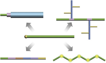
An overview of the current status of nanowire synthesis is shown in Figure 1, which highlights five distinct structural classes available today. The basic semiconductor nanowire structure (center, Figure 1) consists of a uniform composition, one-dimensional (1D) structure with a diameter typically in the range of 3–500 nm. The first work in this area defining a general pathway for nanowire synthesisReference Lieber, Morales, Sheehan, Wong and Yang1, Reference Morales and Lieber2 showed that metal nanocluster-catalyzed vapor-liquid-solid (VLS) growth could be used to grow silicon and germanium nanoscale wires in a controlled manner. In the growth process, which builds upon earlier work showing VLS growth of micrometer to millimeter diameter wires, the nanocluster catalyst forms a liquid solution with nanowire reactant component(s), and when supersaturated, acts as the nucleation site for crystallization and preferential 1D growth. Within this framework, it is straightforward to synthesize nanowires with different diameters and compositions using the appropriate nanocluster catalysts. Soon after the initial report, we demonstrated that this conceptual framework could be used to create nanoscale wires of virtually any uniform composition or alloy semiconductor from the main group of the periodic table.Reference Morales and Lieber2, Reference Duan and Lieber4, Reference Lieber59, Reference Hu, Odom and Lieber60
Basic semiconductor nanowire classes realized by nanocluster-catalyzed vapor-liquid-solid growth. (center) Parent nanowire structure consists of uniform composition and doping (green) and diameter; the nanocluster catalyst (golden) is highlighted at the left tip of the structure. (clockwise from lower left) Axial nanowire with composition and/or doping (indicated by different colors) modulated during elongation of the structure; core/shell or coaxial nanowire with composition and/or doping (indicated by different colors) modulated by sequential two-dimensional shell growth following axial elongation; branched or tree-like nanowire with unique composition and/or doping branches are elaborated by sequential nanocluster-catalyzed growth; and a kinked-nanowire with structurally coherent “kinks” introduced in a controlled manner during axial elongation.

With the nanocluster-catalyzed growth formalism in hand, it has been possible to elaborate the basic nanowire structure in many new and sometimes unexpected directions. In early 2002, my groupReference Gudiksen, Lauhon, Wang, Smith and Lieber13 and several other laboratories around the worldReference Law, Goldberger and Yang68, Reference Thelander, Agarwal, Brongersma, Eymery, Feiner, Forchel, Scheffler, Riess, Ohlsson, Goesele and Samuelson69 first demonstrated that it was possible to synthesize structures in which the composition and/or doping were modulated along the nanowire axial or growth direction (lower left, Figure 1). Later that same year,Reference Lauhon, Gudiksen, Wang and Lieber15 we showed that composition and/or dopant modulation could be encoded in the radial direction with core/shell nanowire structures (upper left, Figure 1). This core/shell nanowire structural motif has proven exceptionally powerful for a wide range of electronic and photonic device applications.Reference Lauhon, Gudiksen, Wang and Lieber15, Reference Qian, Li, Gradečak, Wang, Barrelet and Lieber23, Reference Lu, Xiang, Timko, Wu and Lieber25, Reference Qian, Gradečak, Li, Wen and Lieber27, Reference Li, Xiang, Qian, Gradečak, Wu, Yan, Blom and Lieber29, Reference Qian, Li, Gradečak, Park, Dong, Ding, Wang and Lieber31, Reference Xiang, Lu, Hu, Wu, Yan and Lieber74–Reference Hu, Xiang, Liang, Yan and Lieber79 A third basic motif involves the synthesis of branched or tree-like nanowire structures using sequential nucleation of nanowires from a nanowire backbone (upper right, Figure 1), where each generation of nanowire branches can have a unique diameter and composition.Reference Wang and Lieber17, Reference Jiang, Tian, Xiang, Qian, Zheng, Wang, Mai and Lieber34, Reference Thelander, Agarwal, Brongersma, Eymery, Feiner, Forchel, Scheffler, Riess, Ohlsson, Goesele and Samuelson69
More recently, we have shown that one can break from linear 1D structures and the branched-linear motif to one in which topological centers are synthetically introduced in a controlled manner (lower right, Figure 1).Reference Tian, Xie, Kempa, Bell and Lieber33 In this latter direction, we demonstrated that iterative control over nucleation and growth leads to kinked or zigzag nanowires, in which the straight sections are separated by triangular joints and where doping can be varied at these topologically defined points. Moreover, new workReference Tian, Cohen-Karni, Qing, Duan, Xie and Lieber56 has shown that it is possible to control the stereochemistry of adjacent kinks in a manner that allows the synthesis of increasingly complex two- and three-dimensional structures akin to organic chemistry, thus opening up a great opportunity for the future in terms of designed synthesis.
Functional properties encoded through synthesis in core/shell nanowires
Historically, the first core/shell nanowire structures were synthesized from different combinations of germanium and silicon with a goal of creating new building blocks for nanoelectronics devices.Reference Lauhon, Gudiksen, Wang and Lieber15 For example, the basic structure consisting of a single-crystalline and dopant-free nanowire core of germanium capped with an ultrathin epitaxial silicon shell has proven to be a remarkable system for both conventional and quantum electonics.Reference Lu, Xiang, Timko, Wu and Lieber25, Reference Xiang, Lu, Hu, Wu, Yan and Lieber74, Reference Xiang, Vidan, Tinkham, Westervelt and Lieber75, Reference Hu, Churchill, Reilly, Xiang, Lieber and Marcus77, Reference Hu, Xiang, Liang, Yan and Lieber79 This core/shell nanowire system provides a number of advantages compared to homogeneous silicon or germanium nanowires, including (1) the ability to control surface defects and surface states, which are present in almost all nanoscale structures, (2) isolation of conducting nanowire core from substrate inhomogeneity, and importantly, (3) quantum confinement of carriers within the germanium by the larger bandgap silicon shell.Reference Lauhon, Gudiksen, Wang and Lieber15, Reference Lu, Xiang, Timko, Wu and Lieber25, Reference Xiang, Lu, Hu, Wu, Yan and Lieber74
Initial studies of these then new nanowires configured as field-effect transistors (FETs) demonstrated the highest performance nanowire devices, with performance exceeding the best silicon FETs from industry.Reference Xiang, Lu, Hu, Wu, Yan and Lieber74, Reference Hu, Xiang, Liang, Yan and Lieber79 This remarkable performance from a synthesized nanostructure was due to structural perfection that enabled germanium/silicon nanowire transistors to operate close to the fundamental ballistic transport limit. These attractive room-temperature FET properties have also translated to good performance in low-temperature superconducting and quantum devices,Reference Xiang, Vidan, Tinkham, Westervelt and Lieber75, Reference Hu, Churchill, Reilly, Xiang, Lieber and Marcus77 where, for example, this core/shell nanowire system is now recognized as an excellent test bed for exploring solid-state implementations of quantum bits for quantum computing.Reference Hu, Churchill, Reilly, Xiang, Lieber and Marcus77
Nanowire photovoltaics—limits and new concepts
The core/shell structure described previously as well as axial modulated nanowires can be elaborated to investigate a number of scientific problems in new and often unanticipated ways. One issue of particular interest is solar energy conversion using nanostructured photovoltaic devices, which can convert absorbed light into electrical energy. The use of nanowires as photovoltaic elements presents several key advantages.Reference Tian, Zheng, Kempa, Fang, Yu, Yu, Huang and Lieber36–Reference Dong, Tian, Kempa and Lieber39 First, the principle of bottom-up design allows the rational control of key nanomaterial parameters, which will determine photovoltaic performance, including chemical/dopant composition, size, and morphology. Second, single or interconnected nanowire elements can be integrated with conventional electronics and/or nanoscale electronics to provide energy for low-power applications. Third, and critical to our work, studies of fundamental photovoltaic properties at the single nanowire level will permit determination of the intrinsic limits, areas of improvement, potential benefits, and potentially new concepts for such nano-enabled energy conversion devices.
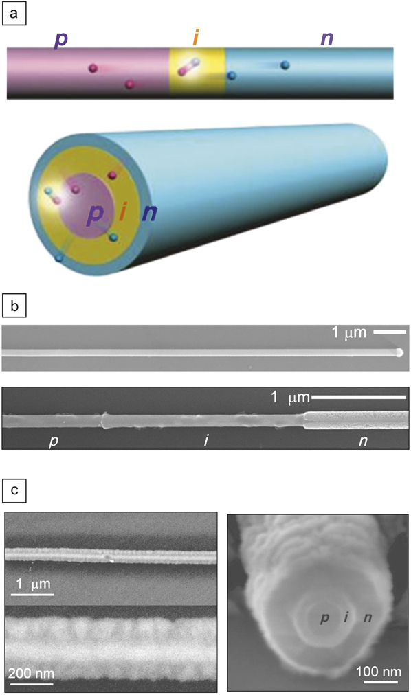
Two unique structural motifs that can yield functional photovoltaic devices at the single nanowire level are shown schematically in Figure 2a. These include p-type/intrinsic/n-type (p-i-n) dopant modulation in axialReference Kempa, Tian, Kim, Hu, Zheng and Lieber37 and radial or core/shellReference Tian, Zheng, Kempa, Fang, Yu, Yu, Huang and Lieber36 geometries. In the axial structure, the active region of the device is located at the position of the p-i-n modulation, while in the core/shell radial nanowire, this active p-i-n interface extends along the entire length of the nanowire. Hence, the core/shell geometry enables collection of photo-generated charge carriers on a much shorter (radial) length-scale than in the axial structure, which, in principle, can lead to higher efficiencies.
(a) Schematics of two distinct motifs for nanowire photovoltaics where the single p-type/intrinsic/n-type (p-i-n) diodes are synthetically integrated in (top) axial and (bottom) core/shell structures. (b) Scanning electron microscopy (SEM) images of p-i-n silicon nanowires. (top) As-grown nanowire with nanocluster catalyst on right tip of nanowire. (bottom) Dopant-selective etched nanowire highlighting the distinct p-, i-, and n-type regions with lengths consistent with growth times. (c) SEM images of a p-i-n coaxial silicon nanowire at different magnifications. Images were recorded with the electron beam (left) perpendicular to the nanowire axis and (right) nearly end on. Adapted from References Reference Tian, Zheng, Kempa, Fang, Yu, Yu, Huang and Lieber36–Reference Tian, Kempa and Lieber38.
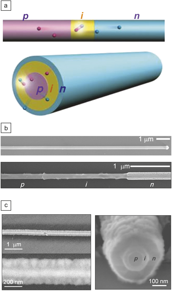
The axial and radial p-i-n photovoltaic nanowire structures were realized first in silicon nanowiresReference Yang, Barrelet, Capasso and Lieber35, Reference Kempa, Tian, Kim, Hu, Zheng and Lieber37 by rational design within the context of the nanocluster-catalyzed VLS growth model. For example, we modulated the dopant from p-type to intrinsic to n-type during axial elongation to create the p-i-n axial structures. Scanning electron microscopy images (Figure 2b) show that with as-synthesized nanowires, the designed active region is realized and is uniform in diameter after dopant-selective etching.Reference Kempa, Tian, Kim, Hu, Zheng and Lieber37 On the other hand, if we change the growth conditions to lower pressure and higher temperature after nanowire elongation, we can switch from an axial growth to a two-dimensional homogeneous deposition and create the p-i-n core/shell/shell structure, as shown in Figure 2c.
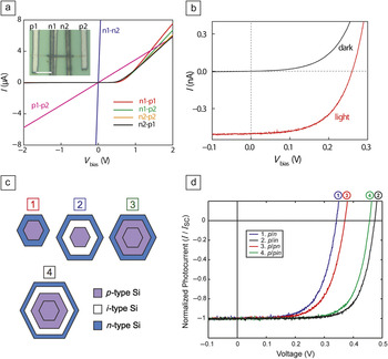
Significantly, studies of photovoltaic devices configured from both structural motifs yield exciting behavior,Reference Tian, Zheng, Kempa, Fang, Yu, Yu, Huang and Lieber36–Reference Dong, Tian, Kempa and Lieber39 although here we will focus on p-i-n core/shell silicon nanowire photovoltaic devices first reported in 2007.Reference Tian, Zheng, Kempa, Fang, Yu, Yu, Huang and Lieber36 Dark current versus voltage (I–V) curves obtained from radial p-i-n devices (Figure 3a) exhibited good diode characteristics, including current rectification for reverse bias voltage and a sharp current onset in forward bias.Reference Tian, Zheng, Kempa, Fang, Yu, Yu, Huang and Lieber36 Linear I–V curves from core–core (p1-p2) and shell–shell (n1-n2) electrode configurations demonstrate that ohmic contacts are made to both core and shell portions of the nanowires, and thus the observed diode characteristics are due to the synthetically encoded radial p-i-n core/shell structure.
(a) Dark current versus voltage (I–V) curves of a p-i-n core/shell device with contacts on core–core, shell–shell, and different core–shell combinations; V bias is the applied voltage. Inset, optical microscope image of the device; scale bar, 5 μm. (b) Dark and light I–V curves recorded for the coaxial nanowire device, where the light curve was recorded under 1-sun illumination. (c) Cross-sectional schematics of four distinct core/shell diode geometries investigated as standalone single nanowire solar cells. The core in all structures is p-type. (d) Normalized (photocurrent/short-circuit photocurrent) light I–V characteristics of single nanowire solar cells corresponding to the four distinct diode geometries shown in (c). Adapted from Reference Reference Tian, Zheng, Kempa, Fang, Yu, Yu, Huang and Lieber36.

Notably, the electrical characteristics of these single core/shell silicon nanowire devices determined under 1-sun illumination (Figure 3b) showed classic photovoltaic device behavior with open-circuit voltages and short-circuit current densities of ca. 0.26 V and 24 mA/cm2, respectively.Reference Tian, Zheng, Kempa, Fang, Yu, Yu, Huang and Lieber36 The product of these parameters is critical in determining the overall device efficiency, and as such serves as a key metric to evaluate when comparing different materials, structures, and devices. For the initial radial p-i-n core/shell structures, the most remarkable feature was the high short-circuit current density, which approached that of the best thin-film silicon devices, whereas the open-circuit voltage was lower than ideal for a good silicon-based photovoltaic device. Nevertheless, this combination led to the highest efficiency (3.4%) from a nano-enabled photovoltaic device at the time.Reference Tian, Zheng, Kempa, Fang, Yu, Yu, Huang and Lieber36
With the results and advances in hand, it was important to ask key scientific questions: What are the limits for these new nanowire photovoltaic structures, and how can we best assess these limits? These questions can be addressed by recognizing that the open-circuit voltage and short-circuit current can be addressed separately in terms of the material junction quality and light absorption, respectively. Focusing first on open-circuit voltage, which was substantially lower in our initial work than possible for an ideal bulk structure, we investigated different junction structures. Specifically, given the capability to grow highly controlled core/multi-shell structures, we designed a series of structures shown in Figure 3c. These structures start from a simple core/shell p/n diode and advance to increasingly complex structures, in which we introduce intrinsic and p-shell layers. It is possible to synthesize such nanowire structures by design in single-crystalline form with nanometer control over the shell thicknesses.Reference Hahm and Lieber41 Indeed, scanning electron microscopy (SEM) images show very sharp faceting, which is indicative of single-crystalline structures. Moreover, cross-sectional high-resolution transmission electron microscopy (HRTEM) and electron diffraction studies demonstrate the high quality of these faceted core/shell nanowire materials.
This series of designed structures represents a unique and well-defined test bed for probing key factors affecting photovoltaic properties. Significantly, I–V measurements recorded under 1-sun illumination (Figure 3d) show a systematic increase in the open-circuit voltage, from about 0.2 V in the initial studies, up to almost 0.5 V, which is approaching the limit that one might expect in a single-crystal silicon photovoltaic cell. Even though we are working on a structures with diameters of only 200–300 nm, which have much higher surface/interface areas than micron and larger scale structures, the intrinsic open-circuit voltage is approaching an ideal value. Hence, design and high-quality growth demonstrate that there are no intrinsic limitations on the open-circuit voltage for nanometer scale photovoltaic devices.
Turning to the second key photovoltaic metric, the short-circuit current density, we have focused on measuring the absolute, wavelength-dependent properties. Overall, the new single-crystalline core/shell structures do not absorb light as efficiently as the nanowire structures reported in 2007Reference Tian, Zheng, Kempa, Fang, Yu, Yu, Huang and Lieber36 and yield short-circuit current densities about a factor of two lower. This is not surprising, because the absorption through single-crystal silicon is much lower than that for the nanocrystalline silicon that comprised the shells of the earlier work. One way to enhance absorption in the new single-crystalline nanowire photovoltaics involves using a reflector layer on the back of the transparent device substrate. These structures yield nearly a two-fold increase in the short-circuit current density and overall efficiencies >6%, which represents a breakthrough for nanoscale ultrathin structures.
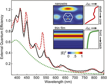
What are the intrinsic limits of these nanoscale photovoltaic devices? This is a particularly interesting question, because there are some unique opportunities in nanoscale structures versus microstructures. To answer this question, we have measured the action spectrum or the photocurrent versus wavelength on single nanowire devices. By making these measurements in a quantitative manner, it is possible to extract absolute external quantum efficiencies and compare these measurements with simulations. For example, the absolute wavelength-dependent external quantum efficiency (EQE), which is determined from these measurements, is highly structured, showing a number of well-defined peaks corresponding to maxima in the light absorption (black line, Figure 4). In contrast, the wavelength-dependent EQE for a thin film of silicon of equal thickness is a much lower and unstructured absorption. Thus and perhaps unexpected, these results show that considerably better performance can be obtained using a nanowire structure. The underlying explanation for these exciting results has been elucidated by finite-difference time-domain (FDTD) simulations. Specifically, simulation of EQE (red dashed line, Figure 4) for the measured core/shell nanowire has near quantitative agreement with the experimental results. Importantly, the observed peaks can be associated directly with resonant cavity modes, either whispering gallery modes or Fabry-Pérot cavity modes, that are unique to the subwavelength diameter nanowire structures. These resonant modes exhibit enhanced electrical fields and corresponding enhanced absorption efficiency relative to uniform silicon structures.
External quantum efficiency (EQE) as a function of wavelength for a p-i-n nanowire (black curve) and simulated EQE spectrum (dashed red curve) produced with no adjustable parameter other than the size of the nanowire (height of 240 nm). Dashed green curve shows the simulated spectrum for the top 240 nm of planar Si. (inset) Plot of electric field intensity for a plane wave (λ = 445 nm) interacting with a Si nanowire (top) and thin film (bottom). White line defines outline of nanowire and top surface of the thin film. To the right are plots of total short-circuit current density (J SC) as a function of position inside the nanowire and thin film.

The really exciting implication of these new results can be readily understood by considering the solar spectrum. Specifically, by changing the nanowire structure—diameter and/or morphology—it is possible to shift the positions of the resonance modes such that one can maximize absorption for a very thin structure. Hence, we now have a truly new concept for improving efficiency in ultrathin photovoltaics unique to a nanoscale structure: tune these resonances through both the diameter and the morphology, and then combine optimized structures by assembly to yield photovoltaics using much less material than would be required by more conventional approaches.
This work represents a great opportunity for the future. Whether this leads to an advance in large-scale photovoltaics is a different question, but that is not the fundamental question we have focused on. The present studies demonstrate that our approach could represent a new one for improving large-scale solar energy conversion. Furthermore, recognizing that electronics in its many guises will be distributed on a smaller scale, we will need small power sources to efficiently drive these devices. In 2007,Reference Tian, Zheng, Kempa, Fang, Yu, Yu, Huang and Lieber36 it was shown to be possible to take a single nanowire photovoltaic of modest efficiency and use it to drive many nano-electronic devices, including a biosensor and logic circuit. Now we have the opportunity to consider not only large-scale power generation, but also the ability to assemble a unique combination of nanowire functional building blocks to build self-powered nanosystems.
Nanowire nanoelectronics/biology interface
As a second example of the potential of nanowires, I will review work focused on the interface between nanoelectronics and biology. Why is it important to merge nanoelectronics with biology? The answer to this question is readily apparent when one recognizes that the natural scale of communication in biological systems is the nanoscale, for example, using nanometer- scale ion channels of electrogenic cells and nanometer-scale macromolecules involved in signal transduction. Therefore, to build a seamless integrated interface between electronics and living biological systems, it is necessary to work at the same level as the biology, which is the nanoscale. If we are able to achieve this goal, we can open up numerous opportunities, from the creation of powerful new tools for conducting fundamental and applied studies to realization of completely new hybrid materials.
Work on the nanoelectronic–biology interface began with studies in early 2000, which were designed to exploit the high surface-to-volume ratio of emerging nanoelectronic FETs as biosensors.Reference Cui, Wei, Park and Lieber40 Notably, these seminal studies demonstrated that functionalized silicon nanowire FETs could serve as exquisitely sensitive detectors for recording changes in solution pH and measuring the binding of proteins with high sensitivity and specificity.Reference Cui, Wei, Park and Lieber40 This work was subsequently extended in a significant manner, for example, by studies demonstrating multiplexed real-time detection of cancer marker proteins, including detection in hundred-billion-fold excess proteins in blood serum, the detection of DNA and DNA mismatches relevant to disease, drug screening and discovery, and detection of single virus particles.Reference Hahm and Lieber41–Reference Patolsky, Zheng and Lieber46 These studies have demonstrated a high degree of robustness and reproducibility for our concept of nanowire nanoelectronic sensors, and thus I believe one of the most important directions in this area should be toward that of commercialization.
In addition, there remain interesting scientific questions to address, including what are the limits of detection, and can nanoelectronic sensors function under physiological conditions of high ionic strength? We have begun to address the first fundamental question in two ways. First, we investigated the detection of single particles in virus sensing studies.Reference Patolsky, Zheng, Hayden, Lakadamyali, Zhuang and Lieber42 These studies showed unambiguously that it is possible to detect single viral particles with excellent signal-to-noise and high selectivity. Second, and more recently, we have investigated limits of nanowire FET detection sensitivity in both linear and subthreshold regimes of an FET.Reference Gao, Zheng and Lieber51 Both of these studies suggest substantial promise for future development of nanowire sensors as single-molecule detectors, which could have a large impact in many areas, including DNA sequencing.
I believe that one of the greatest opportunities lies at the more complex interface between nanoelectronic devices and cells and tissue. Motivation for this area is apparent when one examines, for example, the brain and the way in which it is “wired.” The cells in the brain—neurons—are interconnected by nanoscale synapses, not micron- and larger-scale structures used in the past for building electronic interfaces.Reference Patolsky, Timko, Zheng and Lieber48, Reference Timko, Cohen-Karni, Qing, Tian and Lieber54 Hence, to communicate with the network of neurons at the natural scale in which they communicate, we need nanoscale electronic devices. Initial work to realize this new concept showed that it was possible to create arrays of nanowire FET devices, culture neurons over these device arrays, and then record propagating action potentials following neuronal stimulation.Reference Patolsky, Timko, Yu, Fang, Greytak, Zheng and Lieber47 Moreover, we showed that it was possible to record multiple signals from individual neurons using the nanowire device arrays and thus demonstrate not only artificial synapses but “wiring” (e.g., multiple interconnections/cell) very similar to nature. Nevertheless, a culture of cells on planar arrays of devices is far from natural.
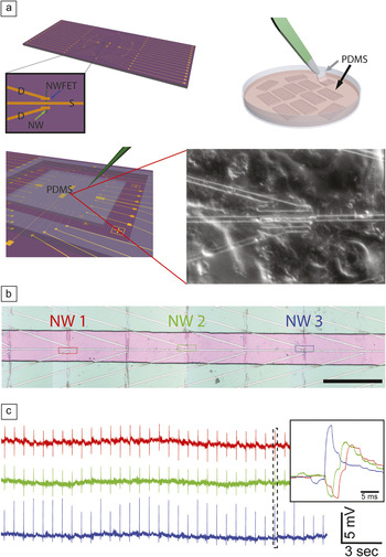
A significant breakthrough was made in 2009 addressing the limits in our initial work.Reference Gao, Zheng and Lieber50 Specifically, we separated these two systems—the nanoelectronic devices and cell arrays—at the initial stage of design and only brought them together later to form the key nanoelectronic/cell interfaces as shown in Figure 5a. In this way, it is possible to design an ideal nanodevice array, whether that device is built on silicon or on a clear and flexible plastic substrate, and optimize this array for a particular experiment independent of cell culture. In parallel, we “built” a cell/tissue sample that is biologically relevant by culturing cells or tissue on a biopolymer or scaffold not constrained by the device chip. The nanoelectronic device and cell/tissue structures can then be brought together and registered at the subcellular level (Figure 5a).
(a) (top left) Nanowire field-effect transistor (NWFET) chip, where nanowire devices are located at the central region of the chip. The visible linear features (gold) correspond to nanowire contacts and interconnect metal. Zoom-in showing a source, S, and two drain electrodes, D, connected to a vertically oriented nanowire (green arrow) defining two NWFETs. (top right) Cells cultured on thin rectangular pieces of poly(dimethylsiloxane) (PDMS), where the black arrow highlights one piece in the culture medium, and the gray arrow indicates one piece being removed with tweezers. (bottom) PDMS piece with cultured cells oriented over the device region of a NWFET chip. The green needle-like structure indicates the probe used to manipulate the PDMS/cell substrate to specific nanowire device locations. (lower right) Optical micrograph of the assembly in cell medium for the area corresponding to the zoom-in in the image on the top left. (b) Optical micrograph showing three NWFET devices (NW1, NW2, NW3) in a linear array, where pink indicates the area with exposed devices; scale bar, 150 μm. (c) Representative conductance versus time signals recorded from spontaneously beating cardiomyocytes by NW1, NW2, and NW3. Inset, high-resolution comparison of the temporally correlated peaks highlighted by the dashed box. Adapted from Reference Reference Cohen-Karni, Timko, Weiss and Lieber50.

This approach was originally demonstrated in studies of cardiac cells in 2009.Reference Cohen-Karni, Timko, Weiss and Lieber50 For example, multiplexed measurements using a linear array of three nanowire devices (Figure 5b) in contact with a spontaneously beating monolayer of cardiomyocyte cells yielded very stable and high S/N (∼10) peaks corresponding to the extracellular signals (Figure 5c). If we examine the peaks recorded at each of the three devices at a specific time, we can see that the beating is not coherent. Rather, there is an excitation wave propagating from right to left, from nanowire 3 to nanowire 1 and, moreover, with these equidistant devices, we can see that the time differentials between devices are not equal. Therefore, we can conclude that there is a resistance in the propagation in the signal from 3 to 2, and it is more efficient from 2 to 1 due to differing cell-to-cell communication.
The limits of extracellular multiplexed recording can also be pushed to a higher density such that it is possible to literally “image” the excitation wave within a single cell. To accomplish this feat, we have synthesized axial modulation–doped nanowires (see Figure 1), where the modulated region defines the active device size, and the pitch between these regions defines device density.Reference Yang, Zhong and Lieber28 Measurements on cardiomyocyte cells have demonstrated several key points in these new studies. First, the temporal width of individual recorded peaks, ∼0.5 ms, is similar to that for which individual sodium ion channels are open during an action potential. Second, it is possible to record measurable time differences between peaks recorded from a single cell, and thus image the propagation of an action potential within one cell. Taken together, these results demonstrate the potential for electrical interfacing with submicron spatial resolution and microsecond time resolution, which together are unprecedented in recording compared to other available electrical or optical methods.
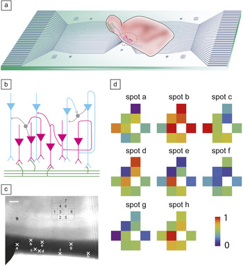
We have also exploited this approach and our nanowire device arrays as powerful tools for investigating the neural circuitry associated with olfaction. Figure 6a illustrates a brain slice oriented over a two-dimensional array of nanowire devices such that the devices are in contact with the cortical region of the slice. This region is involved in the processing of signals from the olfactory bulb, and an understanding of this processing is critical to our understanding of smell.Reference Qing, Pal, Tian, Duan, Timko, Cohen-Karni, Murthy and Lieber52 A schematic of the organization and input circuit of the slice in this region (Figure 6b) highlights the myelinated axon fibers, which carry signals from the olfactory bulb and the synaptic connections with the dendrites from the neurons in the cortical processing region. Elucidation of the transmission and processing of signals within this cortical region is difficult, because conventional techniques can provide either high spatial resolution or high temporal resolution, but not both at the same time.
(a) Overview of a nanowire field-effect transistor (NWFET) array fabricated on a transparent substrate with an acute brain-slice oriented with the pyramidal cell layer over the devices. (b) Laminar organization and input circuitry of the piriform cortex in the region of the brain slice oriented over the NWFET array. (c) Optical image of an acute slice over a 4 × 4 NWFET array. Signals were recorded simultaneously from the eight devices indicated on the image. Crosses along the lateral olfactory tract fiber region (dark band at bottom of image) of the slice mark the stimulation spots a–h. Scale bar is 100 μm. (d) Maps of the relative signal intensity or activity for devices 1–8 obtained following near threshold stimulation at sites a–h. Adapted from Reference Reference Qing, Pal, Tian, Duan, Timko, Cohen-Karni, Murthy and Lieber52.

We have exploited the high-resolution recording capability of the nanowire FETs in 2D arrays to probe the activity patterns of layer neurons in this cortical region when stimulating different sets of axon fibers. In a representative experiment (Figure 6c), eight nanowire devices within a four by four array were used to record from the brain slice following stimulation at eight different positions (a–h) in the bundle of axons. Notably, two-dimensional maps of the neural activity recorded from the eight nanowire devices in the array for each of the eight stimulation positions (Figure 6d) provide new information. First, visual inspection of these maps clearly demonstrates how heterogeneous activity can be resolved. For example, stimulation at spot b is strongly coupled to most regions except those monitored by device 1, while stimulation at spot f is weakly coupled to most regions. Second, comparison also shows very different pair-wise correlations for activity at nearby stimulation points. These results show clearly the potential of our nanowire nanoelectronic arrays for addressing critical neurobiology problems. For example, plasticity of the olfactory system suggests that the neural network is dynamic, and thus our highly localized direct recording could enable visualization of the dynamic and provide information necessary to understand the circuits and plasticity in this and other neural systems.
Synthesis enabling paradigm changes
One of the limitations in interfacing cells with the nanoelectronic devices described previously is that we are recording on the outside of the cell and using this information to understand what is happening on the inside. It would be preferable to record biological processes directly inside a cell. Existing probes capable of intracellular sensing and recording include a single-terminal glass micropipette. The single electrical connection facilitates design and mechanical insertion into cells, but the requirement of direct ionic and/or electrical junctions between probe tips and cell interior also introduces limitations, including (1) a relatively large (>0.2 μm) tip size to enable accurate recording, (2) exposure of the intracellular region to electrolytes in the micropipette probe, and (3) the intrinsically passive nature of the devices compared with active FET devices.
Nanoscale transistors could function as point-like, mechanically non-invasive probes capable of entering cells through natural pathways as can occur with similar sized viruses and nanoparticles, and process input/output information without the need for direct exchange of solution (as occurs in micropipettes). The requirement of two electrical contacts to a FET makes design of 3D probes and their minimally invasive insertion into a cell or tissue a substantial challenge, although conceptually it is possible to relax this geometric constraint of typical FETs by creating a nonlinear or bent nanowire FET structure.Reference Tian, Xie, Kempa, Bell and Lieber33, Reference Tian, Cohen-Karni, Qing, Duan, Xie and Lieber56
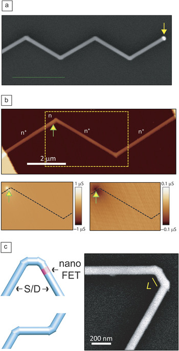
Significantly, this new concept was realized synthetically with the novel synthesis of kinked nanowire structures shown schematically in Figure 1.Reference Tian, Xie, Kempa, Bell and Lieber33 We demonstrated a “nanotectonic” approach that provides iterative control over the nucleation and growth of nanowires and used it to grow kinked or zigzag nanowires in which the straight sections are separated by triangular joints, as illustrated in Figure 7a, a SEM image of a silicon nanowire with five kinks with equal length arms between the kinks.Reference Tian, Xie, Kempa, Bell and Lieber33 By controlling the growth time between kinks, it is also possible to precisely vary the lengths of the straight sections. In addition, we have grown dopant-modulated structures in which specific device functions, including p-n diodes and field-effect transistors, can be precisely localized at the kinked junctions in the nanowires. For example, scanning gate microscopy studies of a double-kink device with dopant modulated only at one of the two kinks (Figure 7b) demonstrated that an active transistor could be synthetically localized by design at a specific topological site on the device. We can thus create by design, for the first time in a nanostructure, electronically functional stereocenters akin to the chemically functional centers that have proved so powerful in molecular organic chemistry and biochemistry.
(a) Scanning electron microscopy (SEM) image of a multiply kinked two-dimensional silicon nanowire with equal ca. 0.8 μm arm segment lengths. The nanocluster catalyst is evident at the right end as the bright/high-contrast dot. (b) Atomic force microscopy (top) and scanning gate microscopy (SGM) (bottom panels) images of one dopant-modulated double-kinked silicon nanowire structure. The SGM images were recorded with a tip-voltage, V tip, of +10 V (left) and –10 V (right). The dark and bright regions correspond to reduced and enhanced conductance, respectively. The black dashed lines mark the nanowire position, and the arrows point to the position of the lightly doped active region of the device. (c) Schematics of 60° cis (top) and trans (bottom) configurations for double-kinked nanowires. The blue and pink regions designate the source/drain (S/D) and nanoscale field-effect transistor (FET) channel, respectively. (right) SEM image of a double-kinked nanowire with a cis kink configuration. L is the length of segment between two adjacent kinks. Adapted from References Reference Tian, Xie, Kempa, Bell and Lieber33 and Reference Tian, Cohen-Karni, Qing, Duan, Xie and Lieber56.

We have used this new synthetic advance to create two-terminal FET probes that can be inserted into single cells.Reference Tian, Cohen-Karni, Qing, Duan, Xie and Lieber56 While it is possible to do so with a single kinked structure, the 120º kink angle is not ideal. Hence, we first focused on incorporating two cis-linked kinked units to yield probe tip angles of 60º, as shown in Figure 7c. Because two trans-linked units (Figure 7c, bottom) would yield an unusable probe tip, the selective synthesis of cis-linked units is central to our probe geometry design. A representative SEM image of an 80 nm diameter, double-kinked silicon nanowire with an intervening segment length (L) of ∼160 nm between kink units showed a well-defined cis-linkage and an overall 60º tip angle (Figure 7c). To investigate our ability to synthesize this cis-linkage of kink structural units reproducibly, we analyzed their fraction as a function of L in double kinked structures. Notably, the plot of cis/(cis + trans) as L was varied from ∼700 to 50 nm and shows that the cis conformation becomes dominant as L decreases, with a yield of ∼70% for L ∼ 50 nm.Reference Tian, Cohen-Karni, Qing, Duan, Xie and Lieber56 Finally, by modulating the dopant during the growth process, it is further possible to introduce nanoscale FETs at the probe tip during overall synthesis.
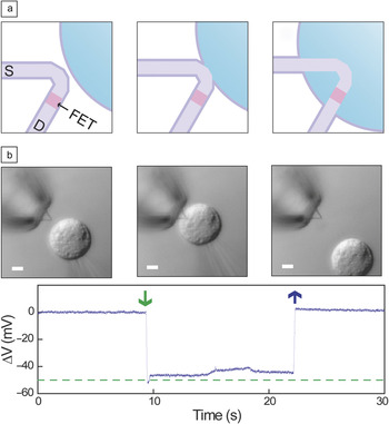
To use the new kinked nanowire FET probes in cells (Figure 8a), we coated them with phospholipid bilayers, since previous studies had shown that these bilayers can form on a variety of nanostructured inorganic materials and also fuse with cell membranes.Reference Chernomordik and Kozlov80 Fluorescence microscopy images of dye-labeled phospholipid modified probes showed that the lipid formed a continuous shell on the nanoprobes. We then monitored the calibrated potential change of the phospholipid-modified nanowire FET probe while an isolated HL-1 cellReference Claycomb, Lanson, Stallworth, Egeland, Delcarpio, Bahinski and Izzo81 was moved into contact and then away from the nanoprobe using a glass micropipette under microscopy visualization (Figure 8b). The micropipette was also used to fix the intracellular potential at ca. –50 mV. Notably, measurement of the potential versus time from the probe shows a sharp ∼52 mV drop within 250 ms after cell/tip contact. While the nanoprobe tip is within the cell, the recorded potential maintains a relatively constant value of ca. –46 mV, and then returns to baseline when the cell was detached from the nanowire probe end. Interestingly, nanowire probes of similar sensitivity that were not coated with a phospholipid bilayer modification exhibited only baseline fluctuations (< ±1 mV), as the HL-1 cell was brought into contact and then retracted, showing that the biochemical state of the nanowire probe surfaces is critical for assisting access to the intracellular region. This biomimetically driven internalization of the nanoprobes is distinct from larger, more rigid probes commonly used for intracellular electrical recording where mechanical forces are used to disrupt the cell membrane.
(a) Schematics of a nanowire probe as it (left) approaches and (middle) contacts the outer membrane surface and (right) enters a cell. Dark purple, light purple, pink, and blue colors denote the phospholipid bilayers, heavily doped nanowire segments, active sensor segment, and cytosol, respectively. (b) Differential interference contrast microscopy images (upper panels) and electrical recording (lower panel) of an HL-1 cell and 60° kinked nanowire probe as the cell approaches (left), contacts and internalizes (middle), and is retracted from (right) the nanoprobe. A pulled-glass micropipette (inner tip diameter ∼5 μm) was used to manipulate and voltage clamp the HL-1 cell. The dashed green line corresponds to the micropipette potential. Scale bars, 5 μm. Adapted from Reference Reference Tian, Cohen-Karni, Qing, Duan, Xie and Lieber56.

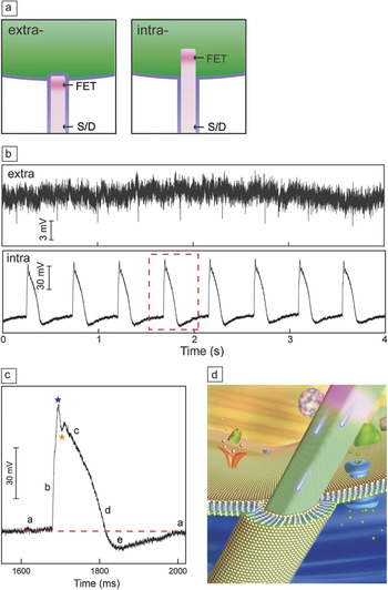
We have also investigated the formation of intracellular interfaces between the kinked nanowire probes and spontaneously beating cardiomyocyte cells, discussed earlier in terms of extracellular recording using conventional nanowire FETs. Conceptually, individual cells are positioned over phospholipid bilayer-modified vertical kinked nanowire probes such that the synthetically integrated FET transitions from extracellular to intracellular positions as the probe is internalized (Figure 9a). Representative data recorded from a nanoprobe initially in gentle contact with a spontaneously beating cardiomyocyte cell showed a sequence of distinct features (Figure 9b). Initially, we observed regularly spaced peaks consistent with the beating cardiomyocyte (Figure 9b). After a relatively brief (∼40 s) period, the initial extracellular signals disappeared, with a concomitant decrease in baseline potential and emergence of new peaks that had an opposite sign, much greater amplitude, and longer duration (Figure 9b).
(a) Schematics of cellular recording highlighting the extracellular (left) and intracellular (right) nanowire/cell interfaces. The cell membrane and nanowire lipid coatings are marked with purple lines. (b) Electrical recording from beating cardiomyocytes: (top) extracellular recording and (bottom) steady-state intracellular recording. The red-dashed box indicates the region selected for (c). (c) Single high-resolution action potential peak recorded with the kinked-nanowire bioprobe. Blue and orange stars designate features that are associated with inward sodium and outward potassium currents, respectively. The letters a–e denote five characteristic phases of a cardiac intracellular potential, as defined in text. The red-dashed line is the baseline corresponding to intracellular resting state. (d) Schematic of a kinked-nanowire electronic sensor probing the intracellular region of a cell. Adapted from Reference Reference Tian, Cohen-Karni, Qing, Duan, Xie and Lieber56.

Detailed analysis of the latter steady-state peaks (Figure 9c) shows five characteristic phases of a cardiac intracellular action potential,Reference Zipes and Jalife82 including (a) resting state, (b) rapid depolarization, (c) plateau, (d) rapid repolarization, and (e) hyperpolarization. In addition, a sharp transient peak (blue star) and a notch (orange star) (Figure 9c) associated with the inward sodium and outward potassium currents can be resolved. These results confirm that electrical recording arises from the highly localized, point-like nanoFET near the probe tip (Figure 9d), which initially records only extracellular potential, simultaneously records both extracellular and intracellular signals as the nanoFET spans the cell membrane, and records only intracellular signals when fully inside the cell.
More generally, these intracellular recordings using nanoscale FET probes represent the first new cell electrical recording technology since the 1970s. While work remains in order to develop this breakthrough nanoprobe as a routine tool, there are already clear advantages: Electrical recording with kinked nanowire probes is simple and eliminates the need for resistance or capacitance compensation; the nanoprobes are less invasive than other intracellular measurement methods (e.g., there is no solution exchange); the small size and biomimetic coating allows for a natural interface between the nonliving/living systems; the nanowire FETs can achieve the highest spatial and temporal resolution during recording; and surface functionalization could open up the real-time measurement of biological species within the cell.
A look to the future: Nanoelectronic-biology frontier
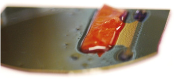
It is interesting to consider how these novel nanoelectronic tools might be used in a broader sense. Specifically, my idea has been to consider the development of a new form of matter—hybrid materials in which we merge 3D nanowire transistor arrays seamlessly together with the tissue. Conceptually, this involves (1) the design and synthesis of the nanowire nanoelectronic device, (2) integration of these devices into a three-dimensional nanoelectronic extracellular matrix or scaffold, and (3) culture of cells within the nanoelectronic matrix to yield a living three-dimensional nanoelectronic tissue. Indeed, incorporation of and culture of cardiomyocyte cells within a three-dimensional nanowire-based matrix yields cardiac tissue hundreds of microns in thickness and innervated with the nanoelectronic network at a scale never before achieved (Figure 10b).
Cyborg cardiac tissue (red) in which a three-dimensional nanowire field-effect transistor network is seamlessly integrated with three-dimensional cultured cardiomyocytes. The width and thickness of the cyborg tissue are ca. 2.5 cm and 1 mm, respectively.

To summarize our emerging vision for the future of the nanoelectronic/biology frontier, consider the following analogy to advances in computing. In the late 1940s and 1950s, the first electronic computers, which used vacuum tubes, were considered to be very powerful, yet as we know today, the advent of the transistor and integrated circuits revolutionized computing in a way perhaps unimagined at that earlier time. Today, biologists and bioengineers have powerful tools available for bridging and making electrical measurements on cells and tissue, but they are all microscale devices and for the most part involve passive electronic recording. Our new advances, where we have merged nanoelectronic transistor devices with cells for the first time, will start the same type of revolution by blurring the distinction between electronics and living cells and tissue.
Conclusions
To summarize, the work done by our group and other groups around the world has shown that semiconductor nanowires are a true platform material. The morphology, structure, and composition of nanowires can be modulated on many length scales by design and at a level that exceeds other nanoscale material systems. This capability of design and synthesis has enabled and will continue to enable the exploration of physical limits of nanostructures, investigating a broad range of scientific problems, discovering and/or uncovering new concepts, and ultimately driving technologies of the future. If we as scientists and engineers stay focused on identifying and tackling these challenges, we will make revolutionary advances in science that truly benefit society.
Acknowledgments
C.M.L would like to express his sincere appreciation to group members who have participated in the studies described in this presentation, as well as collaborators, including Professors Venkatesh Murthy (Harvard), Charles Marcus (Harvard), Hong-Gyu Park (Korea University), Liqiang Mai (Wuhan University of Technology), Dan Kohane (Children’s Hospital), and Robert Langer (MIT). C.M.L. also acknowledges the generous support from the Air Force Office of Scientific Research (AFOSR), Defense Advanced Research Projects Agency (DARPA), Department of Defense National Security Science and Engineering Faculty Fellowship (NSSEFF), McKnight Foundation, MITRE Corporation, and National Institutes of Health Pioneer Award.
Charles M. Lieber graduated with honors in chemistry from Franklin and Marshall College. After doctoral studies at Stanford University and postdoctoral research at the California Institute of Technology, he assumed an assistant professor position at Columbia University in 1987, where he initiated research addressing the synthesis and properties of low-dimensional materials. He moved to Harvard University in 1991 and now holds a joint appointment in the School of Engineering and Applied Sciences and in the Department of Chemistry and Chemical Biology as the Mark Hyman Professor of Chemistry. At Harvard, Lieber has pioneered the synthesis of a broad range of nanoscale materials and characterization of their unique physical properties, the development of methods of hierarchical assembly of nanoscale wires, and the demonstration of key uses of these nanomaterials in nanoelectronics and computing, creating and developing nanoelectronics-biology interfaces, nano-enabled energy, and nanophotonics. His work has been recognized through numerous awards, and he is an elected member of the National Academy of Sciences and the American Academy of Arts and Sciences, and an elected Fellow of the Materials Research Society, American Physical Society, American Chemical Society, and American Association for the Advancement of Science. He is co-editor of Nano Letters, and serves on the editorial and advisory boards of many science and technology journals. Lieber has published more than 320 papers, which have been cited more than 56,000 times, and is the principal inventor on more than 35 patents. In his spare time, Lieber has been active in commercializing nanotechnology, and has founded several nanotechnology companies. Lieber can be reached by email at cml@cmliris.harvard.edu.