Elements of a Faraday rotator
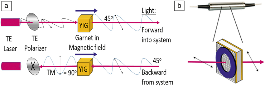
Nonreciprocal optical isolators are necessary and ubiquitous components in optical fiber systems, primarily using Faraday rotation of linearly polarized light to protect laser sources from back reflections, which can cause unwanted noise and instabilities (Figure 1a). Typical implementations of optical isolators involve the assembly of discrete elements into a single optical-fiber-coupled device without waveguiding structures (Figure 1b).1 Integrated photonics is a new field that offers a route to mass production of multiple isolator devices on a single chip, and also to realize photonic integrated circuits (PICs) where lithography and microfabrication are used to define and align elements, similar to electronic integrated circuit (ICs). Unfortunately, isolators and other devices that break time-reversal symmetry are not currently available in PIC systems,Reference Stadler and Mizumoto2 such as silicon-on-insulator (SOI) chips.
(a) Operation of a generic Faraday rotation isolator. Linearly polarized laser light (as transverse electric [TE] modes) propagates forward through a matching polarizer and is Faraday rotated 45° by the magneto-optical garnet before transmission into the optical system (e.g., a fiber-optic network). From the perspective of the source laser, back reflections rotate in the same direction as the forward beam, and are blocked by the polarizer. From the perspective of the propagating light, the rotation has the opposite chirality as it travels forward (with the magnetization of the garnet) versus backward (against the magnetization). (b) Commercial optical-fiber-coupled isolator1 with schematic showing discrete components inside: ring magnet, plastic polarizer film, and magneto-optical garnet films on garnet substrate. Note: YIG, yttrium iron garnet; TM, transverse magnetic.

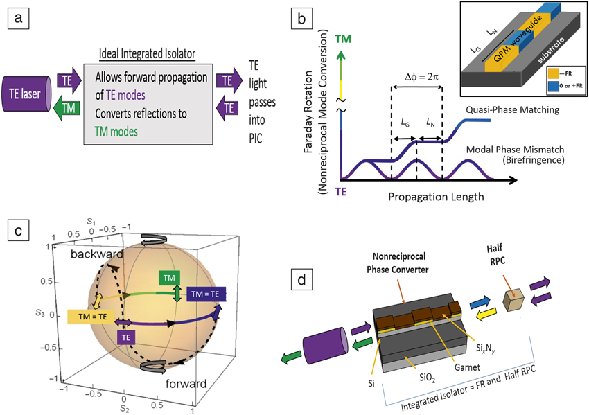
Unlike fiber isolators, PIC devices consist of waveguide structures, and the light is guided in modes whose polarization is defined by the alignment between the electric field of the light and the plane of the chip. Implementing nonreciprocity therefore involves additional complexitiesReference Zhang, Dulal, Stadler and Hutchings3 (Figure 2a). Most integrated lasers emit transverse electric (TE)-polarized modes (the electric field lies predominantly in the plane of the chip), and a majority of integrated PIC devices also operate in the TE mode. An ideal integrated isolator should allow forward propagation of TE-polarized modes, and it should either convert reflections to transverse magnetic (TM) polarization (the electric field lies predominantly normal to the plane of the chip), which does not normally interact with TE-mode (quantum well) lasers, or block reflections altogether.
(a) Ideal integrated isolators should work for transverse electric (TE)-mode light, meaning they allow TE modes to pass into the photonic system (e.g., an integrated circuit [PIC]), and they convert backward propagating light into transverse magnetic (TM) modes, which do not interact with integrated TE-mode lasers. (b) Schematic showing both the effects of phase mismatch (birefringence), shown in the sine-like curve, and the solution—quasi-phase matching (QPM).Reference Zhang, Dulal, Stadler and Hutchings3 QPM can be used to periodically suspend Faraday rotation (mode conversion), step-like curve, by spatially varying the waveguide (inset) with regions of non-Faraday rotating (FR) material, such that the period (L G + L N) corresponds to a modal phase offset of Δϕ = 2π.Reference Zhang, Dulal, Stadler and Hutchings3 (c) Poincaré sphere representation of polarization states of propagating modes in the forward and backward directions, with nonreciprocal (solid lines) and reciprocal (dashed lines) mode conversion. S 1, S 2, and S 3 are Stokes’ parameters. (d) Schematic of silicon-on-insulator integrated isolator using a simple waveguide with QPM garnet claddings for nonreciprocity that is fully TE functional with the addition of a simple half reciprocal phase converter (RPC).Reference Zhang, Dulal, Stadler and Hutchings3

Many proposed integrated isolators use nonreciprocal phase shift (NRPS)—a phenomenon that induces a phase shift in TM-polarized modes using a transverse magnetic field, rather than the longitudinal magnetic field shown in Figure 1. NRPS structures are two-dimensional because they are either branched interferometersReference Shoji, Shirato and Mizumoto4,Reference Ghosh, Keyvaninia, Shoji, Van Roy, Mizumoto, Roelkens and Baets5 or ring resonators.Reference Bi, Hu, Jiang, Kim, Dionne, Kimerling and Ross6,Reference Tien, Mizumoto, Pintus, Kromer and Bowers7 Claddings of magneto-optical garnets (which exhibit NRPS) are introduced to these structures via vacuum deposition, such as pulsed layer deposition (PLD), or wafer bonding, both of which are best suited to depositing the cladding on top of the waveguides rather than on sidewalls. Some attempts have been made to tilt samples during PLD for sidewall coating which enables TE functionality.Reference Pintus, Di Pasquale and Bowers8,Reference Shimizu and Nakano9 More often, these devices require reciprocal polarization converters (RPCs) before and after the isolatorReference Ghosh, Keyvaninia, Shoji, Van Roy, Mizumoto, Roelkens and Baets5 to convert TE modes into TM modes (for NRPS isolation) and then back to TE modes (for transmission into the circuit). Full reciprocal modal conversion is more difficultReference Ghosh, Keyvaninia, Shoji, Van Roy, Mizumoto, Roelkens and Baets5 to implement than half reciprocal conversion,Reference Hutchings and Holmes10 but with just one half RPC and a garnet top-clad waveguide, a Faraday rotation isolator is complete, as described next.Reference Hutchings and Holmes10,Reference Hutchings11
The waveguide equivalent of Faraday rotation is nonreciprocal mode conversion, because the changing polarization is manifested as the light energy flowing from a TE mode into a TM mode. Waveguides are typically birefringent because the propagation constants of the TE- and TM-polarized modes do not match, for example, due to shape anisotropy where the waveguide height is much less than its width. These dimensions are easier to fabricate and are favorable for breaking mode degeneracy, but the modal phase mismatch inhibits nonreciprocal phase conversion, resulting in a periodic behavior of limited magnitude and beat length corresponding to an accumulated modal phase difference of Δϕ = 2π (sine-like curve in Figure 2b).
A simple solution to phase mismatch is quasi-phase matching (QPM),Reference Hutchings and Holmes10,Reference Tien, Martin, Wolfe, Craw and Blank12 which compensates for the phase velocity mismatch and ensures a monotonic flow of energy between the coupled modes (the step-like curve in Figure 2b). QPM requires that the waveguide (Figure 2b, inset) be periodically modulated to suspend Faraday rotation during the downswing of each beat length, as shown. This alternating of magneto-optical garnet with nonchiral materials involves lengths L G and L N, respectively, such that the accumulated modal phase difference Δϕ = 2π (for first-order QPM) over the propagation distance (L G + L N) compensates birefringence.
To visualize the polarization state of the light, Stokes’ parameters (S 1, S 2, and S 3) can be plotted on the surface of the Poincaré sphere, which is shown in Figure 2c.Reference Hutchings and Holmes10 Linear polarization states correspond to the “equator,” circular polarization states correspond to the “poles,” and Faraday rotation is equivalent to moving around the equator. For an isolator, the backward output (e.g., TM polarized) should ideally be orthogonal to the forward injected light (e.g., TE polarized), so the angle between the input and output Stokes vectors is π radians. A full SOI-compatible isolatorReference Zhang, Dulal, Stadler and Hutchings3 involves a QPM cladding on a Si waveguide (Figure 2d). Experimental verification of this design is discussed at the end of this article, where this sphere will be used to explain the state of the light as it travels through the device.
It should be noted that this article deals with SOI photonics so optical properties are all reported for near infrared (1.55-μm wavelength).
Sputter deposition of garnet on nongarnet substrate
The garnets used in optical fiber isolators (Figure 1b) are thick films of yttrium iron garnet (YIG) doped with Bi, Ce, and other elements to improve gyrotropy (a term that includes all nonreciprocal effects, such as Faraday rotation and NRPS), temperature stability, and, in some cases, to provide perpendicular magnetic anisotropy in order to negate the need for a permanent magnet. These films are grown by liquid-phase epitaxy from a molten lead oxide solute, but this process is incompatible with integrated photonics on Si. Initial attempts to grow YIG films on Si-compatible substrates by vacuum processes often resulted in small cracks in the YIG films.Reference Cruz-Rivera, Sung, Cassada, Marrero-Cruz, Stadler, Wehrspohn, März, Noda and Soukoulis13 For early applications, such as proposed bubble memory for computers, these microcracks were somewhat acceptable.Reference Abe and Gomi14 However, light cannot propagate through a garnet waveguide if it contains any cracks, and cracked garnet claddings on Si waveguides would cause unacceptable optical losses.
In 2005, a process was discovered by which YIG could be grown on nongarnet substrates, including Si, by sputter deposition, lithography, and then rapid thermal annealing (RTA).Reference Sung, Qi and Stadler15 This process mitigated thermal-expansion mismatches between SOI-compatible materials ( $\alpha _{SiO_2 } $ = 0.5 ppm/°C, αSi = 2.33 ppm/°C) and garnet (α = 10.4 ppm/°C), and waveguide losses were measured to be less than 1 dB/mm.Reference Sung, Sharma, Block, Keuhn and Stadler16 Attempts to dope this YIG, however, were unsuccessful due to the formation of secondary phases, until thin layers of undoped YIG (prepared similar to the 2005 method) were used as seed layers for pulsed laser deposited (PLD) Ce-doped YIG (CeYIG).Reference Bi, Hu, Jiang, Kim, Dionne, Kimerling and Ross6 It is important to dope YIG because the Faraday rotation, which stems from the off-diagonal components of the dielectric permittivity tensor, is greatly increased (although opposite in sign). For example, the Faraday rotation of undoped YIG in bulk and films has been reportedReference Dulal, Block, Gage, Haldren, Sung, Hutchings and Stadler17 to be +200 degrees/cm, but the (absolute) value is increased to –4500°/cm in sputtered CeYIG on gadolinium gallium garnet (GGG) substrates.Reference Shoji, Mizumoto, Yokoi, Hsieh and Osgood18 For most isolator configurations, the absolute value of the Faraday rotation is more important than the sign, or chirality. For iron garnets, the diagonal terms in the permittivity tensor are the square of the refractive index and have a typical value n 2 = 4.41.
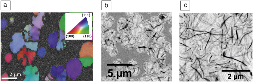
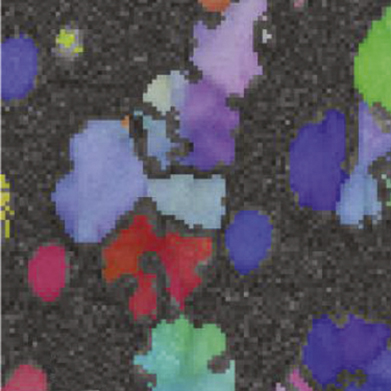
Follow-up studies of seed layer and annealing methods have been conducted by many groups, some of which are covered by Du et al. in this issue. Here, we call attention to two important discoveries—optimal seed layer thicknessReference Block, Dulal, Stadler and Seaton19 via RTA and a two-step anneal to enable thinner seed layers.Reference Gage, Dulal, Solheid, Flannigan and Stadler20 Both of these studies showed the importance of direct observation of crystallinity, for example, by electron backscatter diffraction, (Figure 3aReference Block, Dulal, Stadler and Seaton19) or transmission electron microscopy (TEM), (Figure 3b–c).Reference Gage, Dulal, Solheid, Flannigan and Stadler20 X-ray diffraction alone does not show the presence of nanocrystalline or amorphous phases.
(a) Electron backscatter diffraction image of partially crystallized, very thin (35 nm) yttrium iron garnet (YIG) films.Reference Block, Dulal, Stadler and Seaton19 (b) Bright-field transmission electron microscope images of 25-nm YIG films annealed at only 800°C for 3 min, and (c) first annealed at 400°C for 3 min and subsequently annealed at 800°C for 3 min; the latter being fully crystallized.Reference Gage, Dulal, Solheid, Flannigan and Stadler20 Note: Dark wavy lines, Moiré fringes due to a slight curvature in otherwise perfect YIG crystallites.

Since 2005, RTA has been used as a fast, Si-compatible method to crystallize garnet films. In crystallization studies,Reference Block, Dulal, Stadler and Seaton19 at thicknesses below a minimum value of 45 nm, YIG failed to crystallize fully, which resulted in incomplete crystallization of the CeYIG claddings, as seen in Figure 3a. Seed layers above 45 nm yielded the largest Faraday rotation to date for monolithically integrated CeYIG on Si (–3700°/cm).Reference Block, Dulal, Stadler and Seaton19 Although epitaxial films on GGG have slightly larger gyrotropies, monolithic integration with Si photonics will make upscaling PICs more facile than hybrid integration of garnet-on-garnet.
A second crystallization study showed that very thin (25 nm) YIG films can be fully crystallized without increasing the thermal processing budget (energy requirement) by using a two-step approach.Reference Gage, Dulal, Solheid, Flannigan and Stadler20 In situ crystallization was studied by TEM using laser pulses to anneal 25-nm-thick YIG films. Low-temperature (400°C) “pre-anneals” followed by typical 800°C annealing, enabled YIG crystallites to experience growth fronts of 280 nm/s. In this way, the entire film was crystallized into garnet before the typical nanocrystalline matrix could be formed. These in situ TEM crystallization results were then verified by rapid thermal annealing (Figure 3b–c).
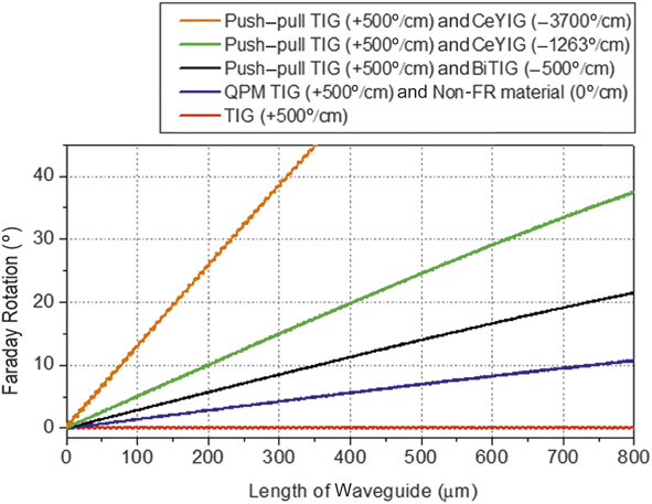
For garnet-core waveguide devices, sputter-deposited films of CeYIG on various seed layers are excellent options for nonreciprocal devices using thick bottom claddings on Si. In fact, full isolation can be achieved with path lengths as short as 350 μm (Figure 4), even when large waveguide birefringence is present.Reference Dulal, Block, Gage, Haldren, Sung, Hutchings and Stadler17,Reference Dulal, Gage, Block, Cofell, Hutchings and Stadler21 As in electronic ICs, small devices are desirable for PICs to achieve more functionality per chip. The structures in Figure 4 are the same as shown in Figure 2b, but here, the “nongarnet” segments are replaced with opposite chirality garnets to create “push–pull” Faraday rotators. In this case, the Faraday rotation is not suspended, but rather, the periodic downswings in the beat-length become upswings to enable devices with short path lengths. For example, undoped TIG has a Faraday rotation (+500°/cm) that is 2.5× larger than for YIG (+200°/cm). Bi doping of TIG (BiTIG) produces a similar magnitude, but opposite chirality Faraday rotation (–500°/cm). As future garnets are discovered with enhanced Faraday rotation of both chiralities, even shorter Faraday rotators will be possible regardless of waveguides birefringence.
Finite-difference time domain simulations of terbium iron garnet (TIG) and quasi-phase matching (QPM) with different combinations of push−pull garnet waveguides (using Bi-doped TIG [BiTIG] or Ce-doped TIG [CeTIG]) with 1.6 μm × 0.8 μm cross sections. The QPM segments (see Figure 2b) are 3.85 μm long and devices are on fused quartz substrates.Reference Dulal, Block, Gage, Haldren, Sung, Hutchings and Stadler17

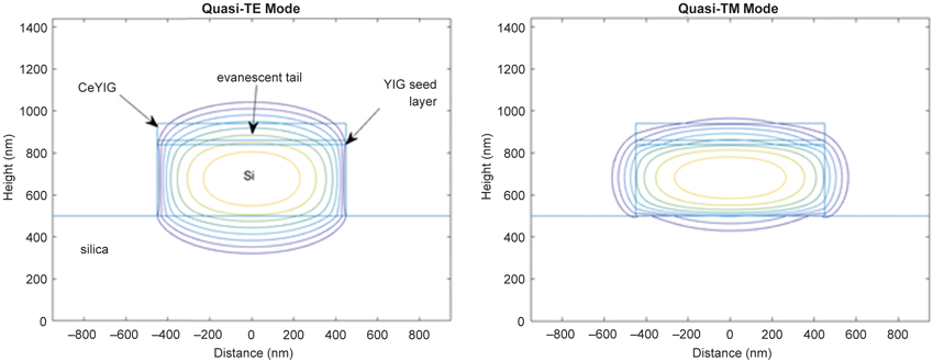
A large number of integrated photonic devices have been realized with SOI platforms where light propagates inside Si-core waveguide devices. Si has diagonal permittivity tensor components of n 2 = 11.7, so there will be large reflections at any interface that requires the light to propagate from a Si core to a garnet core. Therefore, garnet-clad SOI waveguides are necessary to provide isolators for Si PICs, whether those isolators use NRPS or Faraday rotation. However, the best CeYIG films on Si are made using a seed layer that is located between the Si and the CeYIG (Figure 5). When using CeYIG as a cladding, isolation is dependent on the interaction between the evanescent field of the light that “leaks” outside the Si core into this cladding. As shown in Figure 5, the evanescent interaction decreases exponentially with distance from the Si core, so a dilemma is introduced—thin seed layers are desired to enable more evanescent interaction with the Faraday rotation of the CeYIG cladding, but thicker seed layers are needed to fully crystallize CeYIG (and therefore obtain higher Faraday rotation). Sidewall coatings were previously mentioned for TE-mode NRPS operation, but this simulation shows the waveguides will also need careful design to enable side “leakage” for this to work. For direct contact between CeYIG cladding and Si core, new top seed layersReference Sun, Du, Goto, Onbasli, Kim, Aimon, Hu and Ross22 and creative geometries have also been used to avoid mid-structure seed layers, but device fabrication will be greatly simplified using seed layer-free garnet.
Transverse mode profiles for the quasi-TE and quasi-TM fundamental modes in a 340 nm × 900 nm silicon-on-insulator waveguide with 20-nm yttrium iron garnet (YIG) seed layer and 80 nm of CeYIG as an upper cladding. The irradiance contours are shown at –3 dB intervals. Note: TE, transverse electric; TM, transverse magnetic.

Undoped and doped terbium iron garnets (TIGs)Reference Dulal, Block, Gage, Haldren, Sung, Hutchings and Stadler17,Reference Dulal, Gage, Block, Cofell, Hutchings and Stadler21 meet this need of not requiring a seed layer to form on Si. Also, the chirality of the rotation of BiTIG matches CeYIG, and therefore, it could be better as a CeYIG seed layer than undoped YIG.Reference Dulal, Block, Gage, Haldren, Sung, Hutchings and Stadler17 Interestingly, despite the low values of Faraday rotation, BiTIG has been shown to enable higher performance in SOI devices than CeYIG (see next section). Seed layers introduce extra annealing and extra lithography steps, so single-deposition TIG-based films are gaining popularity. CeTIG has recently been reported with Faraday rotations of –2600°/cm,Reference Dulal, Gage, Block, Cofell, Hutchings and Stadler21 and this material is now being explored as a cladding on many proprietary SOI designs.
Faraday rotation in SOI waveguide devices: All-mode isolation
TE-mode SOI-integrated isolators were recently realized with a uniform longitudinal magnetization causing Faraday rotation.Reference Zhang, Dulal, Stadler and Hutchings3 These SOI Faraday rotation isolators were similar in length to TM-mode NRPS Mach–Zehnder interferometers and ring resonators, but the isolators are essentially one-dimensional (1D) (all in a continuous line), which allows high device densities. Faraday rotation isolators only require two elements for TE-mode operation: a Faraday rotator and a half reciprocal polarization converter (RPC) (Figure 2d). Recall that an ideal isolator must transmit TE-mode light from the laser into the PIC chip. But it must also convert all (unwanted) back reflections from the chip into TM-mode light so that these reflections will not interfere with the performance of the laser. The Faraday rotator is designed to allow half of the light energy to flow into the TM mode in the forward direction (purple to blue equator motion in Figure 2c). The half RPC is used to convert the (TE = TM) output of the Faraday rotator back to full TE mode before the light continues into the photonic integrated circuit (lower dashed curve in Figure 2c). This half converter is more straightforward to realize than a full converter.Reference Cruz-Rivera, Sung, Cassada, Marrero-Cruz, Stadler, Wehrspohn, März, Noda and Soukoulis13 Any backward traveling light propagates first through the half RPC and then through the Faraday rotator (top dashed curve, then yellow to green equator motion in Figure 2c). So, these reflections first split their energy (TM = TE) and then Faraday rotate to full TM modes before they reach the laser, leading to a Stokes’ vector angle of π radians (the difference between S 1 = 1 and –1). An additional waveguide polarization-selective element could be included between the laser and the Faraday rotator, as in Figure 1, but here, the polarization selectivity of the quantum well laser itself makes it essentially transparent to TM-polarized light at the wavelength of operation.
Quasi-phase matching (Figure 2b) was accomplished by periodic liftoff lithography of the garnet cladding,Reference Hutchings, Holmes, Zhang, Dulal, Block, Sung, Seaton and Stadler23 and then by coating the waveguide with SixNy for approximate index matching to produce segment lengths corresponding to the characteristic beat length (L G + L N). Silicon-on-insulator (340-nm-thick Si) deep-reactive-ion-etched waveguides were patterned using electron-beam-written poly(methyl methacrylate) masks with liftoff after garnet deposition. Several garnet claddings were used, including CeYIG on YIG (45 nm) and seed layer-free BiTIG (80-nm thick). The best results were obtained with BiTIG,Reference Zhang, Dulal, Stadler and Hutchings3 even though simulations had indicated that the CeYIG claddings should perform better.Reference Dulal, Block, Gage, Haldren, Sung, Hutchings and Stadler17 Presumably this was due to the simplicity of fabrication, which minimizes errors from multiple lithography and annealing steps.
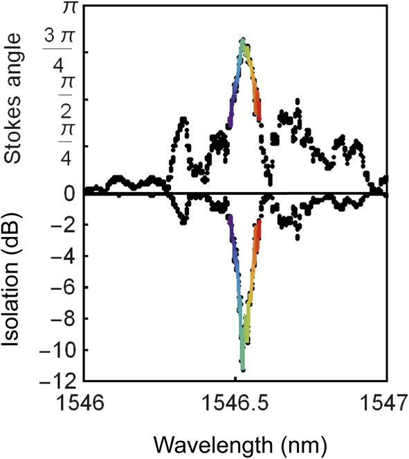
Isolation by nonreciprocal photonic devices is reported as the ratio between TM-polarized transmission in the forward and backward directions (isolation ratio), which is usually inferred from the equivalent measurement of the difference in TM-polarized forward transmission when the transverse magnetic fields are reversed. This measurement eliminates error caused by experimental variations when coupling light into the input or output of the device. A Stokes’ vector angle of 0.83 π was found for the best of the first-generation Faraday rotation isolators that were 3.4 mm long.Reference Zhang, Dulal, Stadler and Hutchings3 Optimization is underway, but even for these nonoptimized devices, simply extending the device lengths to 4.1 mm would be appropriate to obtain a Stokes’ vector angle close to the ideal value of π. The QPM period (L G + L N) corresponding to the results shown in Figure 6 was 8 μm (SOI core: 340 nm × 900 nm), which is a resolution that is easily achieved with standard photolithography. Importantly, with a Stokes vector angle of 0.83 π, a maximum isolation ratio of –11 dB could be obtained,Reference Zhang, Dulal, Stadler and Hutchings3 which is similar to ratios obtained with first reports of TM-mode isolator designs.
Performance of a 340-nm silicon-on-insulator Faraday rotation isolator with seed layer-free BiTIG claddings. (Top) The Stokes’ vector angle of opposite magnetic saturation, where a peak relative angle of 0.83 π is observed. (Bottom) Calculated isolation ratios using these data with an idealized wave plate for reciprocal polarization conversion.

Summary
Similar to the ubiquitous isolators in current fiber-optic systems, Faraday rotators enable source-integrated photonic circuit systems by mitigating reflections to reduce laser feedback and noise. The waveguide equivalent of Faraday rotation, nonreciprocal mode conversion, can be used in 1D (in-line) SOI waveguides simply by providing a top cladding of garnet and a longitudinal magnetic field. Quasi-phase matching can be used to overcome waveguide birefringence while maintaining shape anisotropy, for example, a typical SOI waveguide core (cross section: 340 nm × 900 nm) was clad with alternating segments of CeYIG/YIG or BiTIG separated by segments of SiNx. Successful all-mode (TE to TM) isolators were measured with isolation ratios of −11.6 dB and losses of only 4.6 dB. By extending the length of the BiTIG/SiNx-cladded SOI guides from 3.6 mm to 4.1 mm, simulations show nearly perfect isolation and only 5 dB loss. With these results, source-integrated PICs should be available in the near future.
Acknowledgments
The authors would like to thank the collaborators whose work was reviewed in this article, including C. Zhang, P. Dulal, T. Gage, B. Holmes, D. Flannigan, N. Seaton, A. Block, H. Haldren, S.-Y. Sung, and P. Solheid.

Bethanie J.H. Stadler is a professor and associate head of electrical and computer engineering and a graduate faculty member of chemical engineering and materials science at the University of Minnesota. She earned her BS degree in 1990 from Case Western Reserve University, her PhD degree in 1994 from the Massachusetts Institute of Technology, and was a National Research Council postdoctoral researcher. She has received a National Science Foundation CAREER Award and a McKnight Presidential Fellowship. She served on the MRS Board of Directors and she is currently chair of the MRS Program Development Subcommittee. She taught at the IEEE Magnetic Summer School in Chennai, India, and Assisi, Italy. Her current research focuses on integrating photonic and magnetic materials for photonic isolators, modulators, and sensors. She was a 2015 Distinguished Lecturer for the IEEE Magnetics Society. She is a 2018 MRS Bulletin Volume Organizer. Stadler can be reached by email at stadler@umn.edu.

David C. Hutchings has been a personal chair in optical and quantum electronics at the University of Glasgow, Scotland, since 2004. He obtained his BSc degree in 1984 and his PhD degree in physics in 1988, both from Heriot-Watt University, Scotland. Following postdoctoral research at The College of Optics and Photonics, University of Central Florida, he held fellowships at the University of Glasgow from the Royal Society of Edinburgh and Scottish Office/Executive (1992–1995, 2003) and EPSRC (1995–2000). He is a Fellow of the Institute of Physics and senior member of the Institute of Electrical and Electronics Engineers. His current research focuses on nonlinear optics, monolithic and heterogeneous optoelectronic integration, semiconductor theory and modeling, and computational electromagnetics. Hutchings can be reached by email at david.hutchings@glasgow.ac.uk.