Material issues and considerations
Piezotronic and piezo-phototronic materials possess piezoelectric, semiconducting, and optoelectronic properties.Reference Wang1,Reference Wu and Wang2 Wurtzite structure materials such as ZnO, GaN, and InN have both piezoelectric and semiconducting properties, and thus are most frequently studied. Owing to their noncentrosymmetric nature, semiconductors with the wurtzite structure possess piezoelectric properties that create a piezopotential when strained and can effectively change charge transport across an interface. This effect can be used, for example, in flexible and wearable electronic devices and is anticipated to become an indispensable part of integrated design for future technology. Unfortunately, bulk wurtzite semiconductors suffer from poor mechanical flexibility and thus cannot be used in flexible devices, while the so-called one dimensional wurtzite nanostructures, such as nanobelts and nanowires, that show multifunctional properties for device applications such as optoelectronics, photocatalysis, and energy harvesting are difficult to produce with uniform dimensions and morphologies.
To overcome these limitations of bulk and one-dimensional nanomaterials for piezotronics and piezo-phototronics, two-dimensional (2D) nanomaterials such as monolayer transition-metal dichalcogenides (TMDCs) began to attract great interest due to their combination of semiconducting and piezoelectric properties.Reference Blonsky, Zhuang, Singh and Hennig3 Wu et al. reported the first experimental study of piezoelectric properties of odd-layer 2D MoS2 with a piezoelectric coefficient comparable to that of bulk wurtzite materials.Reference Wu, Wang, Li, Zhang, Lin, Niu, Chenet, Zhang, Hao, Heinz, Hone and Wang4 Interestingly, the piezoelectric coefficient in 2D nanomaterials can be easily modified by varying the chemical composition, molecular structure, and number of layers.Reference Zhang and Meguid5
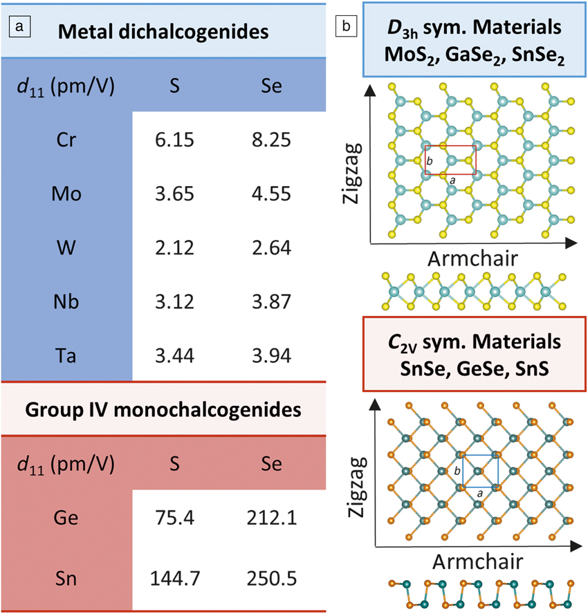
It has been shown that 2D nanomaterials with large anion and small cation polarizability have large piezoelectric coefficients. Zhang et al. reported that the piezoelectric effect in Group IV monochalcogenides (e.g., SnSe, whose linear piezoelectric coefficients e 11 and relaxed-ion (or clamped-ion) coefficient d 11, which can be calculated by the elastic stiffness coefficients C 11, C 12, C 22 as d 11 = (e 11C 22-e 12C 12)/(C 11C 22-C 122), are 34.9 × 10⁻¹⁰ C/m and 2.30 pm/V, respectively)Reference Fei, Li, Li and Yang6 is two orders of magnitude higher than in III–V 2D nanomaterials, 2H-TMDCs (i.e., semiconducting TMDCs with two unit cell layers with hexagonal symmetry), and Group III monochalcogenides (Figure 1a). Molecular structure-dependent piezoelectricity has been observed in Group IV monochalcogenides. For example, there is an axial piezoelectricity response in zigzag structured SnSe, while in the armchair structure, there is a shearing piezoelectric coefficient (Figure 1b).Reference Fei, Li, Li and Yang6 Additionally, piezoelectricity in conjunction with unique electronic and optical properties are easily modified by controlling the number of layers and chemical stoichiometry. For example, in 2H-TMDCs, the piezoelectric effect is only found in odd layered crystals due to the noncentrosymmetry, and the magnitude of the piezoelectric coefficient decreases with the number of layers.Reference Wu, Wang, Li, Zhang, Lin, Niu, Chenet, Zhang, Hao, Heinz, Hone and Wang4,Reference Zhu, Wang, Xiao, Liu, Xiong, Wong, Ye, Ye, Yin and Zhang7
(a) Theoretical piezoelectric coefficient d 11 (units pm/V) in metal dichalcogenides and Group IV monochalcogenides.Reference Zhang and Meguid5,Reference Fei, Li, Li and Yang6 (b) The ball-stick atomic structure of D 3h hexagonal and C 2v orthorhombic monolayers indicating the armchair and zigzag directions, which are defined as the x and y directions, respectively. Red and blue boxes in (b) represent the unit cell. Reprinted with permission from Reference Reference Fei, Li, Li and Yang6. © 2015 AIP Publishing.

The 2D chalcogenides such as 2H-TMDCs and Group IV monochalcogenides are also outstanding semiconductors, hence their bandgaps can be conveniently tuned by modifying the layer numbers and stoichiometry in order to work in the 1.2–1.8 eV spectrum range with excellent mobility at room temperature. Two-dimensional nanomaterials also possess superior mechanical properties that can be used in flexible devices and can sustain large strains, for example, monolayer MoS2 can sustain in-plane strain up to 11% without plastic deformation.Reference Bertolazzi, Brivio and Kis8,Reference Radisavljevic, Radenovic, Brivio, Giacometti and Kis9 Thus, with the combination of remarkable piezoelectric coefficient and electronic, optical, and mechanical properties, 2D nanomaterials are promising candidate materials for piezotronic and piezo-phototronic applications.Reference Wu, Wang, Li, Zhang, Lin, Niu, Chenet, Zhang, Hao, Heinz, Hone and Wang4,Reference Zhang and Meguid5
Fundamental piezotronic process in 2D materials
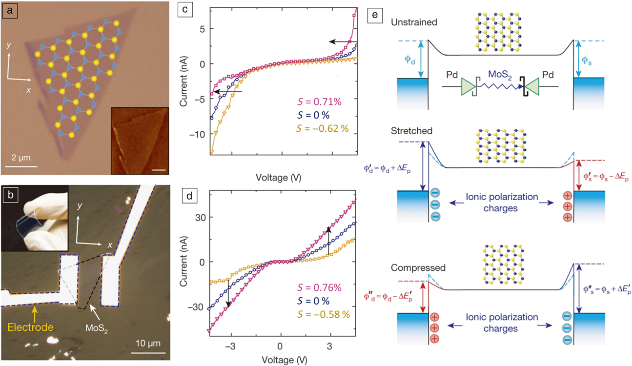
Monolayer 2D TMDCs material such as MoS2 possess distinct in-plane piezoelectricity along the armchair direction. Wu et al. experimentally demonstrated the piezotronic effect in single-layer MoS2 flakes for the first time in 2014, (Figure 2).Reference Wu, Wang, Li, Zhang, Lin, Niu, Chenet, Zhang, Hao, Heinz, Hone and Wang4 By using the second-harmonic generation to determine the crystallographic orientation of mechanically exfoliated monolayer MoS2, the source and drain Schottky contacts were made parallel to the zigzag direction for the maximum piezoelectric response of MoS2 (Figure 2b). The drain current exhibited obvious asymmetrical changes (it increased under positive bias while it decreased under negative bias, or vice versa) under positive and negative bias, regardless of the polarity of strain (Figure 2c). The asymmetric modulation of strain on the drain current confirmed the existence of the piezotronic effect in monolayer MoS2. The uniaxial (tensile or compressive strain along armchair direction) in-plane strain-induced piezocharges, distributed at the two zigzag end edges of MoS2, could effectively serve as the “gate” voltage to modulate carrier-transport behavior and further adjust the drain current through modifying the Schottky barrier heights.Reference Zhang, Liu and Wang10 More specifically, as the monolayer MoS2 device stretches under external mechanical tensile strain deformation along the “armchair” direction, there would be negative and positive in-plane piezocharges generated and accumulated at the source and drain terminals, respectively. As a result, the negative piezocharges could repel the free electrons from the source interface and raise the Schottky barrier height, making it more difficult for the electrons to cross over the barrier and decreasing the drain current under negative bias (under negative bias, the source Schottky barrier was reverse-biased and determined the drain current), whereas positive piezocharges would attract inner electrons and lower the Schottky barrier height at the drain region, leading to a higher drain current under positive bias (Figure 2e).
(a) Optical image of a monolayer MoS2 flake with superimposed lattice orientation derived from second-harmonic generation results. Blue and yellow spheres represent Mo and S atoms, respectively. Inset: atomic force microscope image of the flake. Scale bar = 2 µm. (b) A typical flexible device with monolayer MoS2 flake and electrodes at its zigzag edges. Inset: optical image of the flexible device. (c) The asymmetric modulation of carrier transport by strain (S) under opposite drain bias in a monolayer device. (d) Symmetric modulation of carrier transport by strains under opposite drain bias in a bilayer device. (e) Band diagrams explaining the piezotronic behavior observed in a monolayer device due to the changes in the Schottky barrier heights of the unstrained device by tensile (i.e., stretched) and compressive strain-induced piezocharges. Blue and yellow spheres represent Mo and S atoms, respectively. ϕd and ϕs, Schottky barrier heights formed at the drain and source contacts, respectively; ΔE p and ΔE p′ indicate the change in the Schottky barrier height by piezoelectric polarization charges during stretched and compressed strain, respectively. Reprinted with permission from Reference Reference Wu, Wang, Li, Zhang, Lin, Niu, Chenet, Zhang, Hao, Heinz, Hone and Wang4. © 2014 Nature Publishing Group.

Nevertheless, the drain current of a bilayer MoS2 device presented noticeable symmetrical variation (increased or decreased uniformly) due to the piezoresistive effect when subjected to strain, indicating that the piezotronic effect only occurs in single or odd numbers of layers of MoS2 owing to inversion symmetry breaking (Figure 2d). Qi et al. investigated the intrinsic piezoelectric effect of chemical vapor deposition (CVD)-grown monolayer MoS2 by applying local isotropic deformation through the atomic force microscope.Reference Qi, Lan, Stieg, Chen, Zhong, Li, Chen, Zhang and Wang11 The crystal orientation of a CVD-grown monolayer MoS2 triangle could be easily identified with three zigzag edges. Their results also pointed out that strain-induced in-plane charge polarization could alter the electrical conductivity of the CVD-grown MoS2. The discovery of the piezotronic effect in 2D TMDCs is of great significance for electronics, especially novel electromechanical devices, wearable devices, and human–machine interfaces.
Piezo-phototronics of 2D materials
The direct bandgap in monolayer TMDCs is useful for optoelectronic device applications.Reference Qi, Lan, Stieg, Chen, Zhong, Li, Chen, Zhang and Wang11–Reference Lopez-Sanchez, Lembke, Kayci, Radenovic and Kis13 Through the coupling of optical excitation and the piezotronic effect, piezo-phototronics in monolayer TMDCs, which mainly uses strain-induced in-plane piezocharges or piezopotential to control the transport, separation or recombination processes of photoinduced carriers at the interface of the metal–semiconductor (M–S) contact or p–n junction, may inspire a broad range of applications, such as in photodetectors and solar cells.
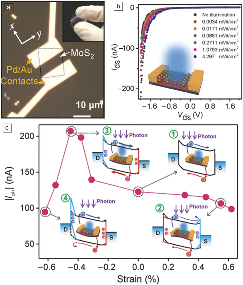
In 2016, Wu et al. reported experimental evidence for the piezo-phototronic effect in single-layer MoS2 and utilized it to improve the performance of a photodetector using this material.Reference Wu, Wang, Yu, Liu, Wei, Hone and Wang14 Figure 3a shows an optical micrograph of the actual device based on mechanically exfoliated monolayer MoS2 on a poly(ethylene terephthalate) flexible substrate. The photoresponse of the MoS2 photodetector under different illumination intensities is shown in Figure 3b, indicating good light excitation characteristics.
(a) Optical micrograph of a flexible single-layer MoS2 photodetector on a poly(ethylene terephthalate) (PET) substrate without strain. Inset: optical image of the flexible optoelectronic device. (b) Photoelectric response of the unstrained monolayer device under different 442-nm light illumination intensities, indicating good light excitation characteristics. The inset: schematic of the MoS2 device under illumination. (c) Strain dependence of photocurrent in the device under an illumination of 4.29 mW cm−2. The insets are device schematics and energy-band diagrams used to explain the working mechanism of the piezo-phototronic response in the monolayer MoS2 photodetector under different strain conditions: (1) unstrained, (2) tensile strain, (3) weak compressive strain, and (4) strong compressive strain.Reference Wu, Wang, Yu, Liu, Wei, Hone and Wang14 An appropriate compressive strain could remarkably increase the photoresponse of the monolayer MoS2 device. Note: I ds, drain-source current; V ds, drain-source voltage bias; I ph, photocurrent; D, drain contact; S, source contact. Reprinted with permission from Reference Reference Wu, Wang, Yu, Liu, Wei, Hone and Wang14. © 2016 Wiley.

The modulation of the photocurrent by strain was further investigated. The relevant results indicate that increasing compressive strain remarkably increased the photocurrent. Interestingly, the photocurrent began to drop once the compressive strain surpassed –0.45%, so the compressive strains needed to be limited in a proper range to obtain the optimized modulation effect for the metal–semiconductor–metal (MSM) structure device. The strain-induced increase in the photocurrent of MoS2 can be explained by the piezo-phototronic effect via an energy-band diagram (Figure 3c). If a suitable compressive strain of approximately -0.4% is applied, a certain amount of negative and positive piezocharges will gather at the source and the drain Schottky barrier, respectively. These piezocharges can adjust the height and width of the two Schottky barriers and thus make it easier for the separation and transport of photo-induced electrons and holes (Inset 3 in Figure 3c).
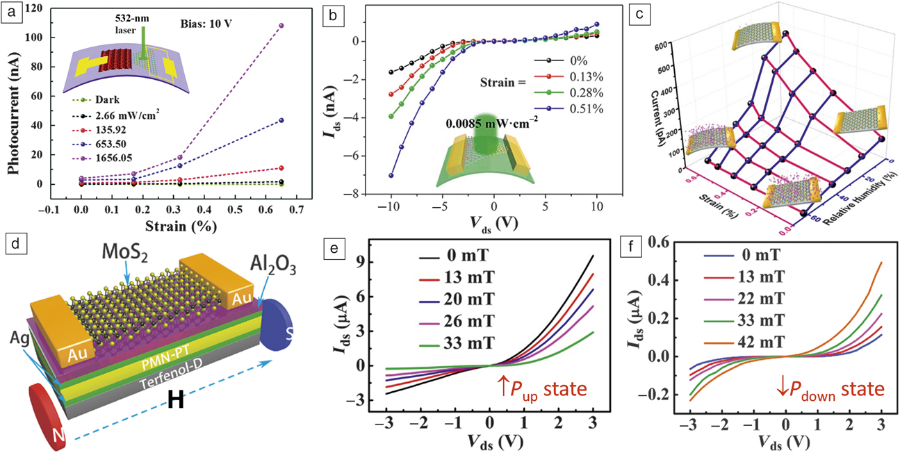
Zhang et al. combined n-MoS2 and p-CuO to fabricate a p–n heterojunction photodetector (Figure 4a), in which the photocurrent was enhanced by a factor of 27 under 0.65% tensile strain by the piezo-phototronic effect apart from using the MSM structure.Reference Zhang, Peng, Wu, Guo, Gao, Liu, Kou, Wen, Lei, Yu, Zhang, Zhai and Wang15 Beyond that, they constructed a monolayer MoS2 p–n homojunction photodiode by p-type chemical doping of MoS2 (Figure 4b).Reference Zhang, Zhai and Wang16 Once an external mechanical tensile strain stimulus of 0.51% was applied to the homojunction device, ultrahigh photoresponsivity and sensitivity were successfully enhanced by 619% and 319%, respectively, which is consistent with the principle of piezo-phototronics. The piezo-phototronic effect in atomically thin 2D materials provides a new way to manipulate the optoelectronic process, which may promote the development of flexible and multifunctional nano-optoelectromechanical systems.
(a) Dependence of photocurrent on strain at different light power densities in the p–n heterojunction photodetector at voltage bias of 10 V, where the photocurrent was maximumly enhanced by 27 times under 0.65% tensile strain. Inset: schematic diagram of the flexible photodetector based on the p-CuO/n-MoS2 heterojunction under a 532-nm laser illumination.Reference Zhang, Peng, Wu, Guo, Gao, Liu, Kou, Wen, Lei, Yu, Zhang, Zhai and Wang15 (b) Photocurrent of the p–n homogenous photodiode under different static tensile strains at 442-nm light illumination intensity of 0.0085 mW · cm−2. Inset: schematic diagram of monolayer MoS2 p–n homogenous diode under light illumination and tensile strain.Reference Zhang, Zhai and Wang16 The photocurrent of the homojunction device increased significantly with the increase of strain. (c) Three-dimensional graph showing the current response of the MoS2 humidity sensor under different tensile strains and relative humidities. Inset: Schematic diagrams of the flexible MoS2 device with respect to different tensile strains and relative humidities.Reference Guo, Wen, Liu, Zhang, Kou, Zhai and Wang17 (d) Three-dimensional schematic diagram of the MoS2-based magnetic-induced piezopotential gated field-effect transistor.Reference Liu, Guo, Yu, Zhang, Kou, Zhang, Wen, Zhang, Zhai and Wang21 I ds–V ds output characteristics with different magnetic fields under (e) P up and (f) P down states of PMN-PT.Reference Liu, Guo, Yu, Zhang, Kou, Zhang, Wen, Zhang, Zhai and Wang21 In these two different states, the magnetic field oppositely modulated the output current of the composite device. Note: I ds, drain–source current; V ds, drain–source voltage bias; P up, polarization up state; P down, polarization down state; PMN-PT, [Pb(Mg1/3Nb)2/3)O3](1−x)-[PbTiO3]x; Terfenol-D, TbxDy1−xFe2 (x ∼ 0.3); N, magnetic North Pole; S, magnetic South Pole; H, magnetic field.

Piezotronic-enhanced 2D materials-based gas sensor
With its ultrathin characteristic at the atomic level, single-layer MoS2 presents a large surface-to-volume ratio, making it more sensitive to the ambient environment. Besides, Schottky barriers can be easily modulated by both surface state and charges at the interface. Combined with this feature, a super-sensitive and flexible monolayer MoS2 Schottky-based humidity sensor was reported. Compared with the strain-free state, its sensing performance could be dramatically improved (1721%) by an external strain due to the piezotronic effect (Figure 4c).Reference Guo, Wen, Liu, Zhang, Kou, Zhai and Wang17 It is believed that other 2D piezoelectric semiconductors also can be applied to such gas-sensing applications by using this principle.
Piezotronics in ferroelectric/2D materials layered composites
Since 2D semiconductor materials are ultrathin, electrons and holes in 2D semiconductor layers can be easily modulated by the surface state of the substrate. Compared with utilizing the inner piezocharges in 2D materials acting as the “gate” voltage to tune the transport behavior of carriers, external piezocharges can also be used to modulate the carrier-transport process in MoS2.Reference Lipatov, Sharma, Gruverman and Sinitskii18–Reference Zhang, Jie, Chen, Liu and Hao20 For example, a magnetic field-induced piezopotential gated field-effect transistor was proposed, which employed external piezocharges triggered by a magnetic field to tune the carrier concentration of MoS2 channel, and further control the drain current (Figure 4d).Reference Liu, Guo, Yu, Zhang, Kou, Zhang, Wen, Zhang, Zhai and Wang21 Under both PMN-PT polarization states, the magnetic field-induced piezopotential could effectively work as a “gate” and further modulate the output current (Figure 4e–f). The composite piezotronic device couples the piezoelectricity of ferroelectric materials and the semiconducting properties of 2D materials, opening up a new route to design and develop hybrid piezotronic devices.
Future prospects
With their excellent mechanical, semiconductor, and piezoelectric characteristics, atomically thin 2D materials, in particular, 2D TMDCs, have demonstrated tremendous potential for low-power flexible micro-nanoelectronic and optoelectronic devices. Meanwhile, the discovery of the piezotronic and piezo-phototronic effects in 2D TMDCs represents a significant milestone in developing next-generation adaptive electronic and optoelectronic devices. Besides 2D TMDCs, other 2D semiconductor materials such as tellurene and α-In2Se3 also show the piezoelectric effect due to their noncentrosymmetric structure.Reference Xue, Zhang, Hu, Hsu, Han, Leung, Huang, Wan, Liu, Zhang, He, Chang, Wang, Zhang and Li22,Reference Wang, Qiu, Wang, Huang, Wang, Liu, Du, Goddard, Kim, Xu, Ye and Wu23 The coupling between piezoelectricity and semiconducting properties in 2D materials makes it possible for external mechanical strain to modulate the transport properties of carriers and the output current, achieving perfect electromechanical conjunction. Furthermore, composite piezotronic devices, which associate ferroelectric materials with 2D semiconductors, may become an important branch of piezotronics. The piezotronic and piezo-phototronic effects in 2D materials provide an excellent opportunity for exploring novel microelectromechanical and optical nanoelectromechanical systems. With the rapid developments in 2D semiconductor materials and devices, we expect to see more advances in research and applications of piezotronics and piezo-phototronics in 2D materials.
Acknowledgments
This work was supported by the National Key R&D Project from the Minister of Science and Technology, China (2016YFA0202703), NSFC (51472056), and the Recruitment Program of Global Youth Experts, China.

Yudong Liu is a postdoctoral candidate at the Beijing Institute of Nanoenergy and Nanosystems, Chinese Academy of Sciences, China. He received his PhD degree in materials science from the Chinese Academy of Sciences in 2018. His research focuses on composite micro-nanopiezoelectric devices based on two-dimensional materials. Liu can be reached by email at liuyudong@binn.cas.cn.

Erlin Tresna Nurlianti Wahyudin is a doctoral candidate in the Department of Materials Science and Engineering at King Abdullah University of Science and Technology, Saudi Arabia. She received her MS degree from the National Cheng Kung University, Taiwan, in 2014. Her research focuses on exploring two-dimensional (2D) materials characterization of and applications in piezoelectric devices and photostriction. Her research also focuses on synthesizing organic–inorganic hybrid 2D materials. Wahyudin can be reached by email at erlin.nurlianti@kaust.edu.sa.

Jr-Hau He is an associate professor in the Department of Electrical Engineering at King Abdullah University of Science and Technology, Saudi Arabia. His research focuses on two-dimensional materials electronics and photonics and solar fuels, and he conducts highly interdisciplinary research to bridge the gaps between research fields and between academia and industry. He is a Fellow of the Royal Society of Chemistry and SPIE, and a senior member of IEEE and OSA. He can be reached by email at jrhau.he@kaust.edu.sa.

Junyi Zhai is a professor in the Micro-/Nanopiezoelectric Materials and Devices Group at the Beijing Institute of Nanoenergy and Nanosystems, Chinese Academy of Sciences, China. He is also the deputy director of the Center on Nanoenergy Research, Guangxi University, China. His research focuses on the fundamental and technological investigation of functional materials and multifield coupling for applications in electronics, sensors, and energy. He has authored more than 90 journal articles with more than 3000 citations. Zhai can be reached by email at jyzhai@binn.cas.cn.