I. INTRODUCTION
A smart reconfigurable antenna unit which can sense the spectrum condition and accordingly reconfigure its characteristics is highly demanding for cognitive radio (CR) application to enhance the system performance and facilitate interoperability between different services. Such antenna unit has a spectrum-sensing antenna for detecting the spectrum condition and reconfigurable antenna for communication purpose [Reference Mansoul, Ghanem, Hamid and Trabelsi1–Reference Tawk, Bkassiny and Christodoulou3]. Further to decrease the system size, these two antennas must be optimally integrated on a single substrate. A lot of antenna designs have been already reported in the literatures which are compatible with CR [Reference Sharma and Tripathi4–Reference Tawk, Bkassiny, El-Howayek, Jayaweera, Avery and Christodoulou8], but only a handful of techniques based on integration concept of these antennas are reported in literature [Reference Sharma and Tripathi9–Reference Hussain and Sharawi20]. In all the reported designs, the numbers of reconfiguration features are limited and further upgradation of these antennas to increase the reconfiguration states are quite challenging because of limited space constraints on board. Now, to obtain more degree of freedom for the selection of different services in a small unit, a new antenna design is required. The physical size of this antenna must also follow the downsizing trend of the system unit, so multiple reconfigurable functionalities must be integrated in a single unit. However, none of the reported antennas can integrate the spectrum-sensing condition with multiple reconfigurable features to meet the essential characteristics of CR system.
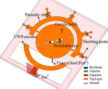
Therefore, here, an integrated versatile antenna with spectrum-sensing capability along with various reconfigurable features is proposed in this paper. Integration of UWB antenna and reconfigurable antenna on single substrate is done in such a way that each printed part is used multiple times in different operating modes. The architecture of proposed antenna consists of a circular patch and a parasitic circular ring around the periphery of circular patch as shown in Fig. 1. The designed antenna senses the spectrum by integrating a UWB antenna from 2 to 11 GHz. After recognizing the spectrum condition, the proposed antenna can reconfigure its frequency state, polarization state, bandwidth and radiation pattern. The frequency reconfigurability is achieved by using a varactor diode from 2 to 4 GHz. Polarization reconfigurability is obtained by using a switchable slot in the circular antenna at 3.9 GHz. Pattern reconfigurability is obtained by designing switchable shorting posts on parasitic arc. For reconfiguring the operating bandwidth from UWB to NB, active state of port is switched. Using these multiple reconfigurable features, user can take more than one benefit of any reconfiguration combinations in a single antenna.
Architecture of proposed integrated antenna.

The challenging goal in this work is to integrate UWB antenna and reconfigurable antenna on a single substrate without disturbing the characteristics of each other; to solve the problem of mutual coupling, UWB antenna is precisely placed physically far away from circular antenna in electro-magnetically quite zone. Complete design evolution, design strategy used, and working principle to design the proposed antenna are thoroughly discussed in the next sections.
II. ANTENNA DESIGN EVOLUTION
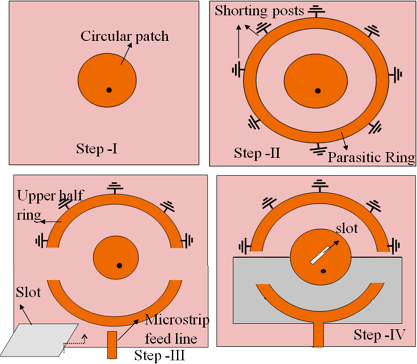
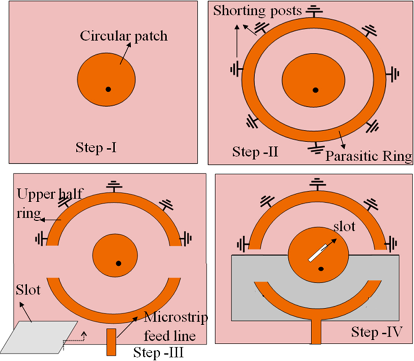
The design strategy used to integrate UWB antenna and various reconfigurable features in a single structure is discussed here. The main focus of the design is to obtain multiple reconfigurable features using the small printed area of antenna as optimally as possible. The complete description of design evolution is explained in four major steps as follows. In the first step, a circular patch antenna is designed which is excited by a coaxial probe. In the second step, a parasitic ring is designed and optimized around the periphery of circular antenna without degrading the S 11 parameter. Now, to add pattern reconfigurability, switchable shorting posts are designed and optimized on the parasitic ring. By shorting the parasitic ring, electric field in the substrate changes, which effectively changes the radiation pattern. In the third step, design is further improved to integrate a separate UWB antenna by reusing its printed area. For this, parasitic ring is divided into two independent parts such that its lower half portion can be reused to realize another separate antenna. The physical separation between circular and UWB antenna is mandatory to ensure no interaction between both antennas. For this, the lower half semicircular ring is pulled 10 mm down from its original position and structure is excited by standard 50 Ω microstrip feed-line. To confirm the UWB characteristics, the ground area beneath the lower portion of the parasitic ring is etched. In this way, a complete UWB antenna is realized and this adds cognitive capability to the antenna. In the fourth step, polarization reconfigurability is added by inserting a switchable slot at the center of the circular patch. Further, to add frequency reconfigurability, a varactor diode is mounted inside the slot. By reverse biasing the varactor diode, the associated capacitance changes, hence the resonant frequency is changed. Detailed geometry description and antenna working principle for each mode are explained later (Fig. 2).
Major design steps for complete evolution of proposed integrated antenna.
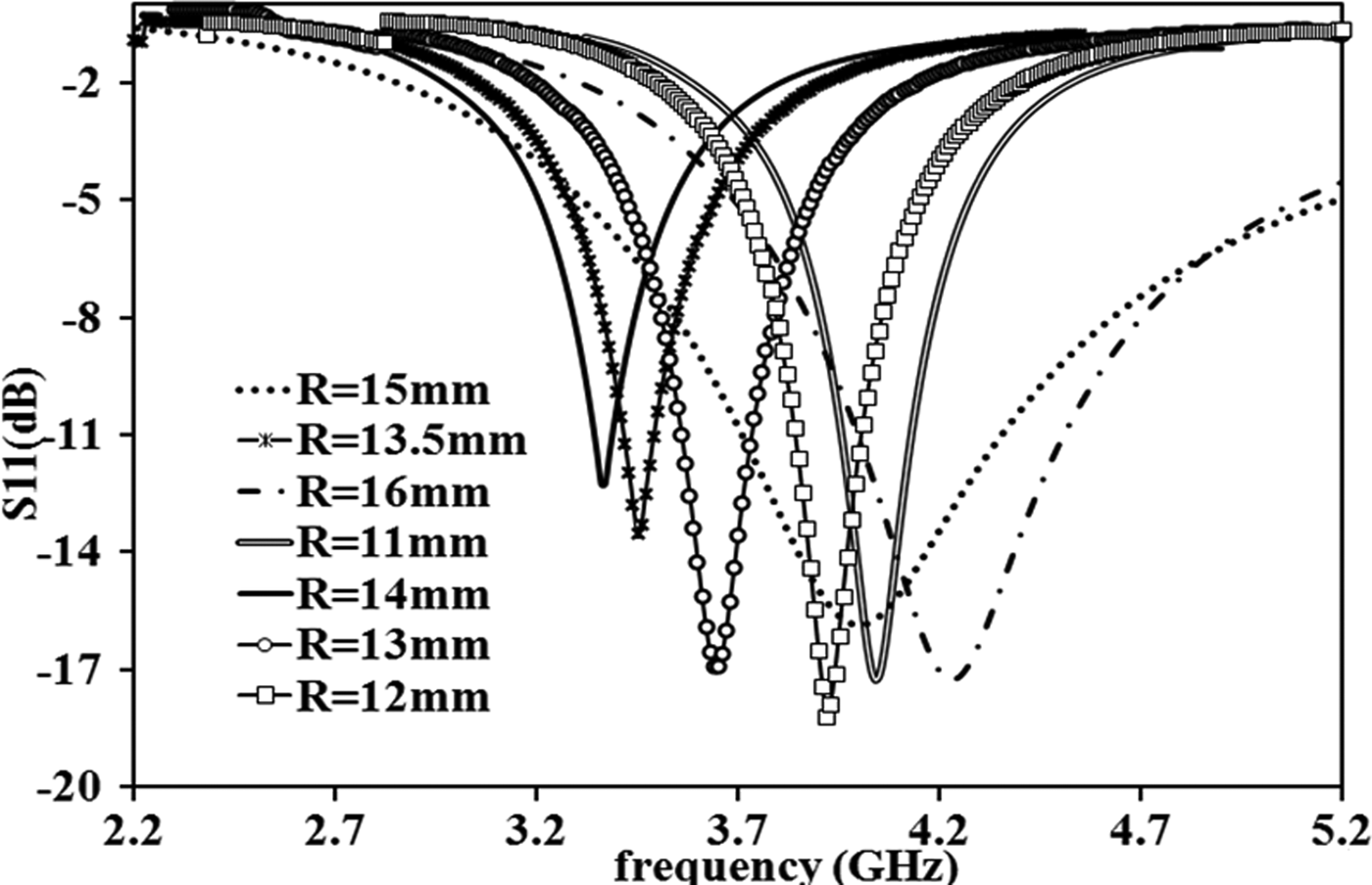
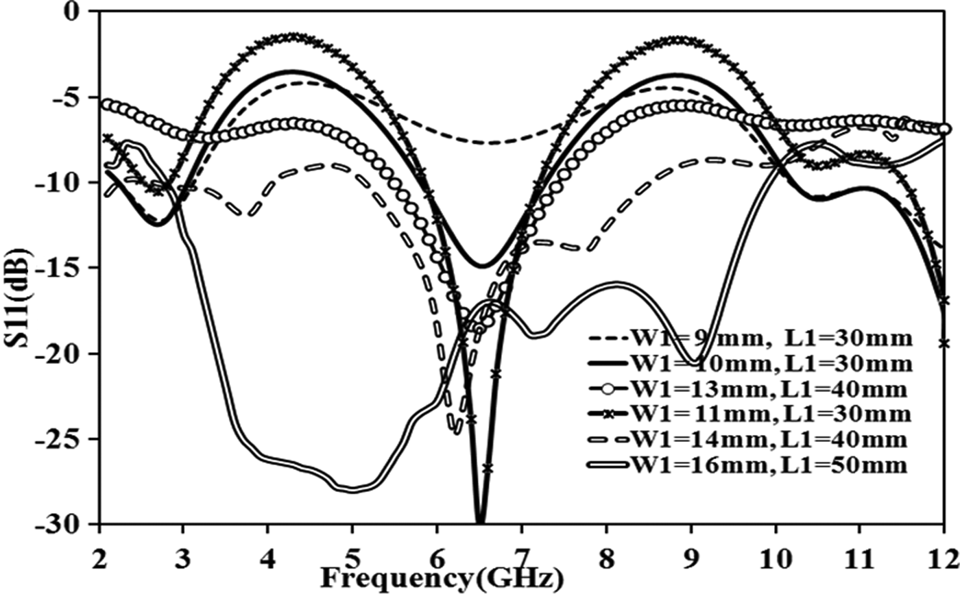
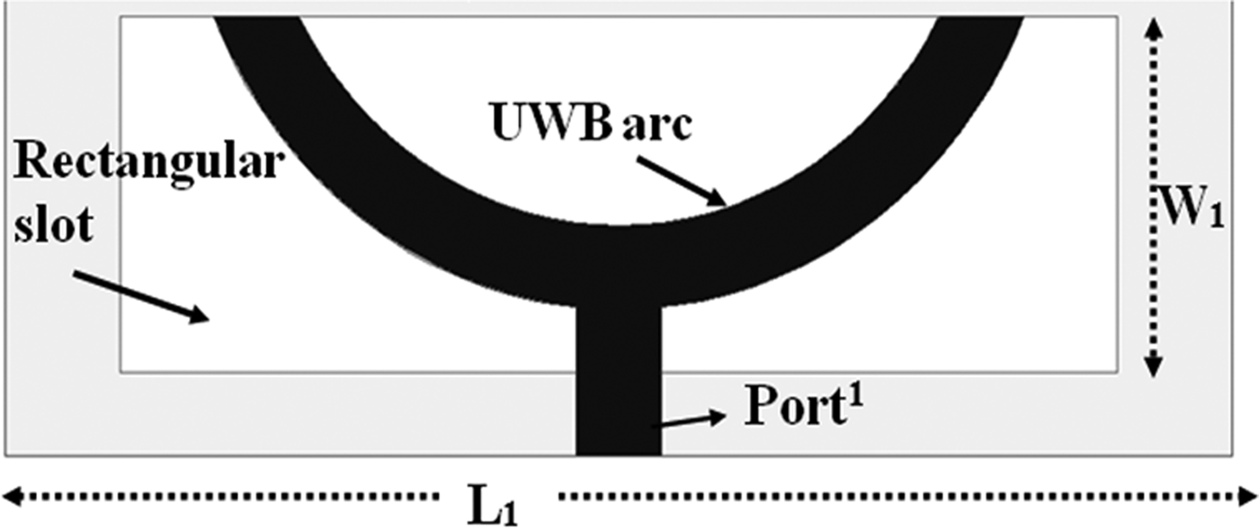
It is observed that addition of reconfigurable feature, biasing lines, equivalent circuit model of PIN diode and varactor diode, etc. alter the equivalent geometry of the antenna which results in degradation of performance of antenna in terms of shifts in resonant frequency and return loss (RL). So, fine tuning of circular antenna and UWB antenna structure is required after the finalization of geometry layout. Figure 3 shows the effect of variation in radius of circular antenna on S 11 parameter. The best observed value of RL = 19 dB at 3.9 GHz for radius R = 12 mm. Figure 4 shows the effect of variation of length and width of rectangular slot under UWB antenna on S 11 parameter. The optimum value of slot dimensions are L 1 = 50 mm, W 1 = 16 mm for UWB operation from 2 to 11 GHz.
Effect of variation of radius of circular antenna.

Effect of variation of length and width of rectangular slot under UWB arc.

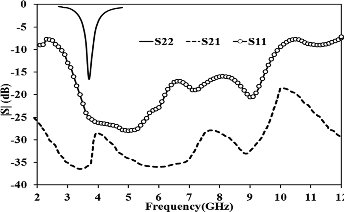
The proposed antenna senses the spectrum via a UWB antenna and reconfigures its various features via a circular antenna. The integration of both antennas is done such that the UWB antenna and reconfigurable antenna work independently without interfering each other's characteristics. For this, UWB antenna is placed either in electromagnetic quite zone or physically far from circular antenna. In this work, UWB antenna is placed in low current density area of circular antenna (inert area to be discussed in the next section) and also enough physically apart. The physical separation between two antennas ensures no interaction between the radiation patterns. Figure 5 shows the S parameter versus frequency for both input ports. The S 21 is better than 25 dB in the entire UWB range, so there is no interaction of RF energy between two ports and both antennas work independently without interfering each other's characteristics. So, there is no need of extra port isolation circuit because there is no transmission of RF power in each operating modes.
S parameter versus frequency for port isolation.

III. WORKING PRINCIPLE
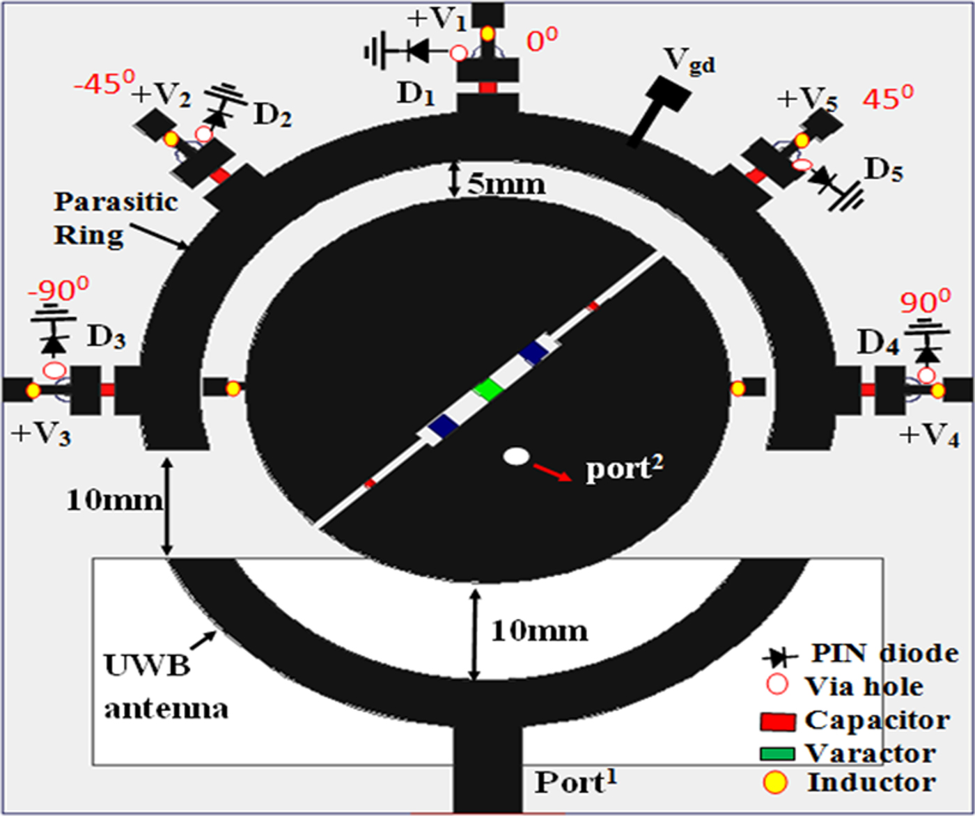
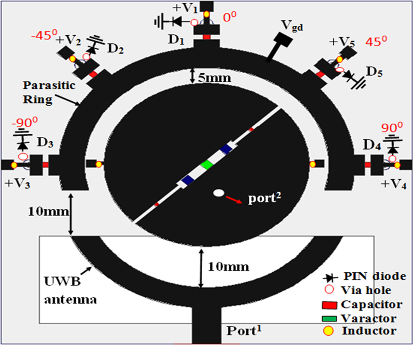
The detailed geometry description of the proposed antenna is shown in Fig. 6. The antenna is designed on Rogers's 5880 substrate with a thickness of 1.575 mm, permittivity of 2.2, and tangential loss of 0.0009. The main radiating circular patch is excited by coaxial probe feed (port 2) at point “A” where the impedance is 50 Ω. A 3 mm wide parasitic ring encloses the circular patch at a distance 5 mm away from its outer edge. Five PIN diodes (D 1 to D 5) are soldered at 45° apart along the circumference of parasitic ring. A wide gap of 10 mm is placed to separate upper half ring and circular antenna from the lower half circular ring. The SMD capacitors provide RF wave connectivity, whilst still maintaining the separation of direct current (DC) form biased PIN diode to unbiased diodes to ensure unwanted poor biasing of other diodes. SMD inductors are used to isolate DC power supply from RF signal.
Layout of proposed integrated reconfigurable antenna.
The proposed antenna design operates in multiple modes namely spectrum-sensing mode, frequency reconfiguration mode, NB-UWB reconfiguration mode, polarization reconfiguration mode, and radiation pattern reconfiguration mode. This section discusses about the working principle of the proposed antenna in these different operating modes.
A) Spectrum-sensing/wideband mode
Figure 7 shows the active portion of integrated antenna when operated for spectrum sensing or wideband mode. A standard 50 Ω microstrip feed line (port 1) is used to convert this passive semicircular arc into an active UWB antenna. The impedance bandwidth is enhanced by optimizing the feed length, shape, size, and location of rectangular slot in the ground plane collectively. The effect of rectangular slot's size in the ground plane is studied in previous section. Figure 4 shows the consequence of different length and width of slot on S 11 parameter and best value slot dimensions are selected for optimum operation in this mode.
Active portion of integrated antenna in spectrum-sensing mode.

B) Pattern reconfigurability mode
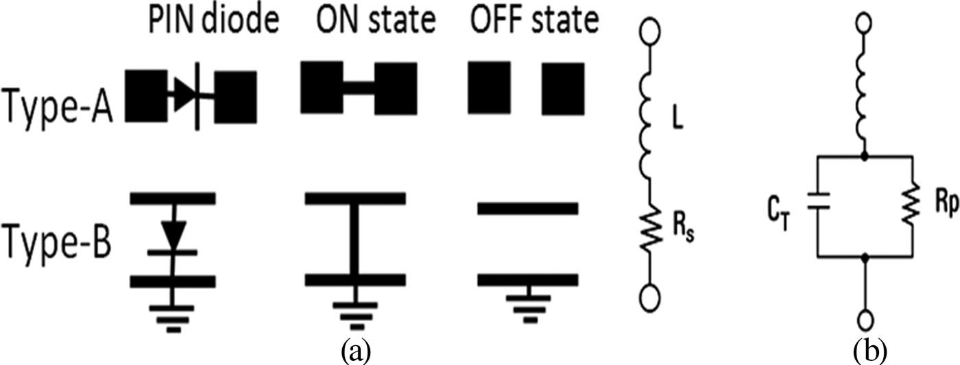
It is an established fact that to realize pattern reconfiguration, direction of pattern should shift at constant resonant frequency. The shape and direction of radiation pattern strongly depends on current distribution in substrate along with the shape and size of radiating antenna. So, in this mode, direction of the pattern is shifted by changing the current distribution in the substrate without shifting the resonant frequency. So, to implement the concept of pattern reconfiguration in the proposed design, a parasitic ring is designed around the circular patch antenna. As this ring is not directly attached with the main patch, so it will not change the resonant frequency. The electric field in the proposed antenna has been changed by shorting the parasitic ring using five switchable shorting posts at specific position. Therefore, in the proposed design, diodes D 1 to D 5 are integrated at 0°, ±45°, ±90° positions around the periphery of the parasitic ring. These diodes are used to short the parasitic ring at the appropriate position. In the proposed design, BAR 64-02 PIN diodes are used to control the flow of RF signal through the structure. Figure 8 shows the equivalent model of ideal PIN diode which exhibits zero resistance to current flow in the ON state and infinite resistance to current flow in the OFF state. So, it can be used to open and close the connection between two metal strips on a single layer (type-A) or between two layers (type-B) as shown in Fig. 8(a). The equivalent model of PIN diode in forward bias and reverse bias is shown in Fig. 8(b). In forward bias, diode is modeled with a forward resistance of 2.1 Ω and inductance = 0.6 µH, and in reverse bias, it is modeled with a reverse parallel resistance = 3 KΩ, capacitance = 0.17 pF, and inductance = 0.6 µH. In Ansoft HFSS simulation, PIN diodes are modeled using lumped RLC boundary to add and analyze the effect of actual PIN diodes.
PIN diode equivalent circuit in (a) ideal case (b) practical case.

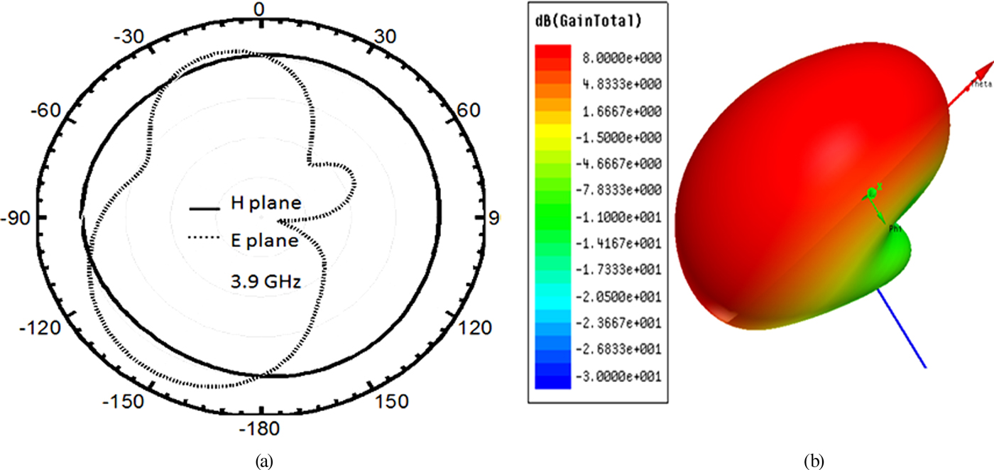
Six different cases for radiation pattern reconfiguration are studied by controlling the different short positions using diodes D 1 to D 5. Under ideal condition, circular antenna emits maximum radiation intensity in 140° direction in ϕ = 0° plane and nearly omni-directional pattern for ϕ = 90° plane as shown in Fig. 9(a). The gain of antenna is 6 dB at 3.9 GHz; its 3D gain pattern is shown in Fig. 9(b).
Simulated (a) E and H planes, (b) 3D pattern for gain at 3.9 GHz.
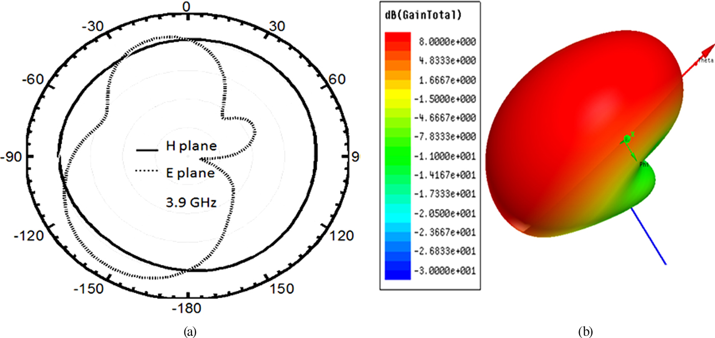
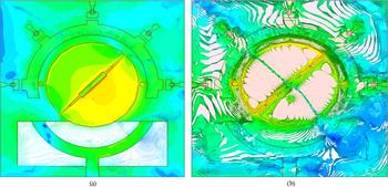
Figure 10 shows the current distribution on the proposed design in ideal condition (no short present). The current distribution is high on circular patch and on the semicircular arc (yellow color) as indicated by Fig. 10(a). The magnitude of current distribution in the substrate is shown in Fig. 10(b). The presence of short on the parasitic ring results in the reformation of the field distribution leading to a shift of the main beam direction away from the short position. In all cases, change in the direction of the beam is defined by the combined effect of location of short and basic radiation patterns of circular patch in ideal case. Generally, a null appears opposite to the position where the short is placed, but due to uneven distribution of the electric fields by various components like presence of another short, their DC bias lines, presence of slot in the ground plane, the pattern can radiate in any direction with any shape. So, the short position must be adjusted to achieve the desired beam direction for more accuracy. The simulation results indicate that direction of main beam can be created anywhere without any definite order or shape in E plane.
Magnitude of current distribution on (a) top layer, (b) substrate.

C) Polarization reconfiguration mode
To generate a circular polarization (CP) wave in the antenna, two equal and orthogonal modes must be excited simultaneously. The proposed CP antenna is designed to generate right-hand circular polarization. For this orientation of RF, current should show complete clockwise rotations in the entire slot or circular antenna. If there are counter clockwise rotations, it will lead to high cross-polarization and deterioration of AR. In this design, an optimized slot of 0.8 mm wide and 12 mm long tilted at +45° is embedded at the center of circular patch to fulfil the necessary condition of CP generation as shown in Fig. 11.
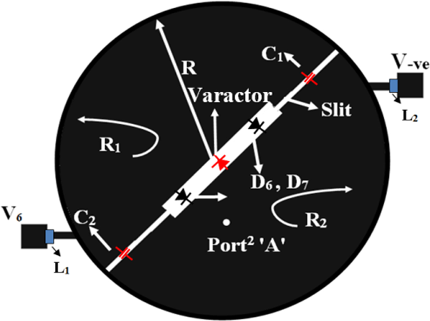
PIN and varactor diode biasing scheme in the circular antenna.
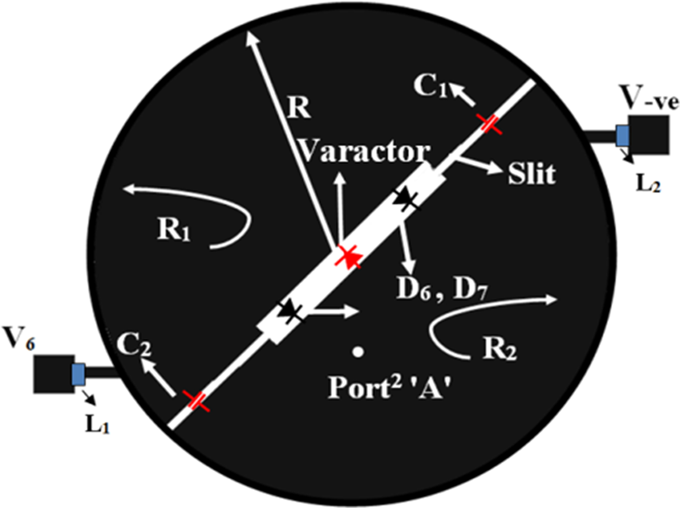
If this slot can be switchable (slot present or absent), one can also switch the polarization state of antenna. To implement this concept, two PIN diodes D6 and D7 are embedded across this slot which makes the slot switchable. A thin slit of 0.3 mm is also etched in the circular patch which divides it into two regions R 1 and R 2 which ensures DC isolation between V 6 and V −ve signal. In between the slit, two SMD capacitors C 1 and C 2 are used for RF continuation and DC isolation. When both diodes are OFF, slot is present and it will produce two orthogonal modes for CP wave. The diodes are forward biased by applying 2V on DC voltage pad V 6 and ground signal on V −ve pad. When both diodes are ON, it will disturb the slot structure, so it will not produce two orthogonal modes, thereby it produces linear polarization (LP) wave.
D) Frequency reconfiguration mode
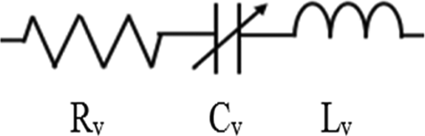
To reconfigure the frequency, a varactor diode is directly integrated in the center of slot of main circular antenna. The Metelics 3001 SMTV (Surface Mount Tuning Varactor) varactor diode with tuning range 0.5–2.25 pF for 30 V > V dc > 0 V is used here [21]. When varactor diode is reverse biased, the junction capacitance varies from 2.25 to 0.5 pF which correspond to different electrical lengths, hence it corresponds to different resonant frequency. In the design, reverse DC bias voltage is varied continuously through two chip inductors on two DC pads V 6 and V −ve. In doing so, PIN diodes D 6 and D 7 are also forward biased and give LP wave but do not interrupt the functioning of varactor diode. The forward breakdown voltage for PIN diodes is much larger, so reverse basing of varactor diode cause no harmful effect on PIN diodes [22]. Two SMD capacitors (30 pF) maintain RF continuity across isolated regions R 1 and R 2. Two coil-craft SMD inductor are placed near DC pad, so that there is very low leakage toward DC. Figure 12 shows the equivalent model of varactor diode considered during simulation. The value of R v = 1.6 Ω, C v = 0.5 to 2.2 pF, L v = 0.4 nH for varactor diodes. In simulation, parametric analysis is conducted using HFSS software to add capacitor loading effect from 2.25 to 0.5 pF.
Equivalent model of varactor diode.

E) Bandwidth reconfigurability mode
The another important feature of the proposed antenna is that in addition to spectrum-sensing mode, the semicircular arc can be used as a UWB transmitting antenna. Now the user can take the benefits of UWB technology as well as reconfigurable technology in a single unit. Moreover, antenna can reconfigure its operating bandwidth either in UWB mode or any NB by switching the active port state. The proposed antenna will work for UWB mode if port 1 is activated and it can switch its bandwidth in NB mode if port 2 is activated.
IV. RESULT AND DISCUSSION
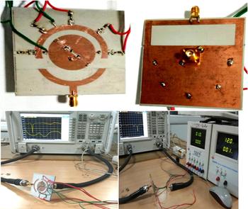
Reconfiguration mechanism in each mode is explained and verified experimentally. Fabricated prototype and experimental setup for proposed antenna is shown in Fig. 13. MITS PCB Prototyping Machine is used for the fabrication of proposed integrated antenna. In the fabricated prototype Coil Craft Inductors, Murata SMD Ceramic Multilayer Capacitors, Infineon BAR64-02 PIN diodes, and Metelics varactor are used. The S parameters of proposed antenna are measured using Agilent N5222A VNA. The radiation pattern of the antenna is calibrated in an anechoic chamber using a standard horn antenna. The proposed integrated antenna AUT (antenna under test) is used as receive antenna and placed on the positioner with required elevation and azimuth coverage. The physical separation between horn antenna and AUT is approximately far field distance R = 2D 2/λ where R = separation distance between transmit and receive antennas, D = aperture of AUT, and λ = shortest wavelength. Different radiation patterns in xy-plane and xz-plane are measured by switching the short position on parasitic ring manually. To reconfigure the short position, high resistivity nichrome wires are used to interconnect portable DC power battery and DC bias pad on AUT. These high resistivity wires reduce the current flow in the transmission lines to avoid re-radiation and messing up radiation patterns of antenna. Portable DC power battery is also covered with microwave absorber to mitigate the unwanted effect on the radiation pattern. The transmitted and receive power is measured to calculate the gain of AUT using Friis formula. The comparison of results for each operating mode is described as follows:
Fabricated prototype and experimental setup.

A) Spectrum-sensing mode
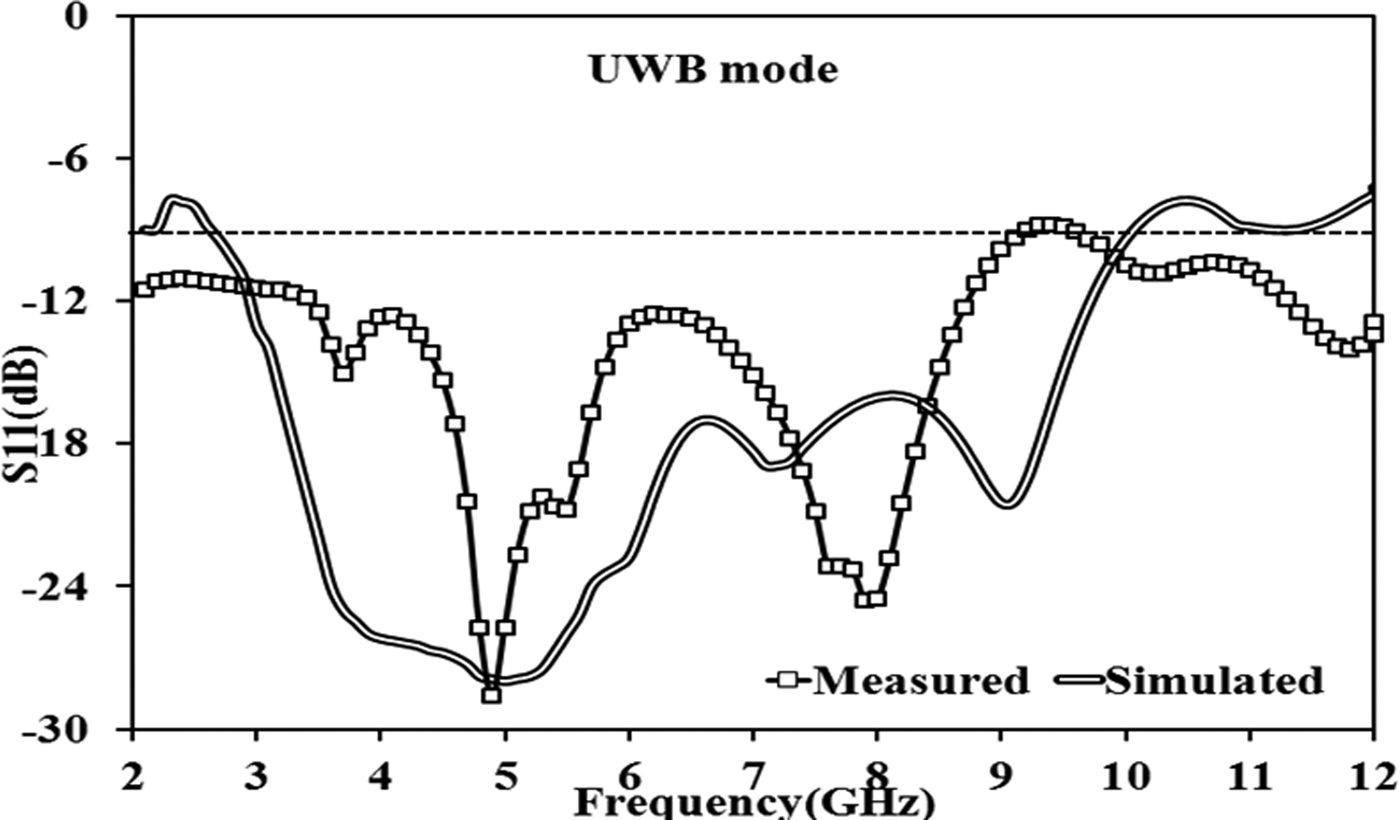
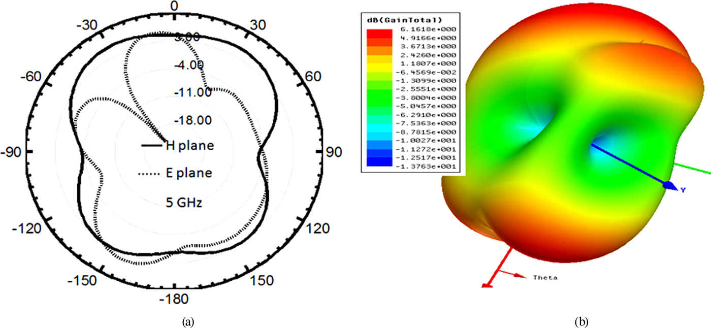
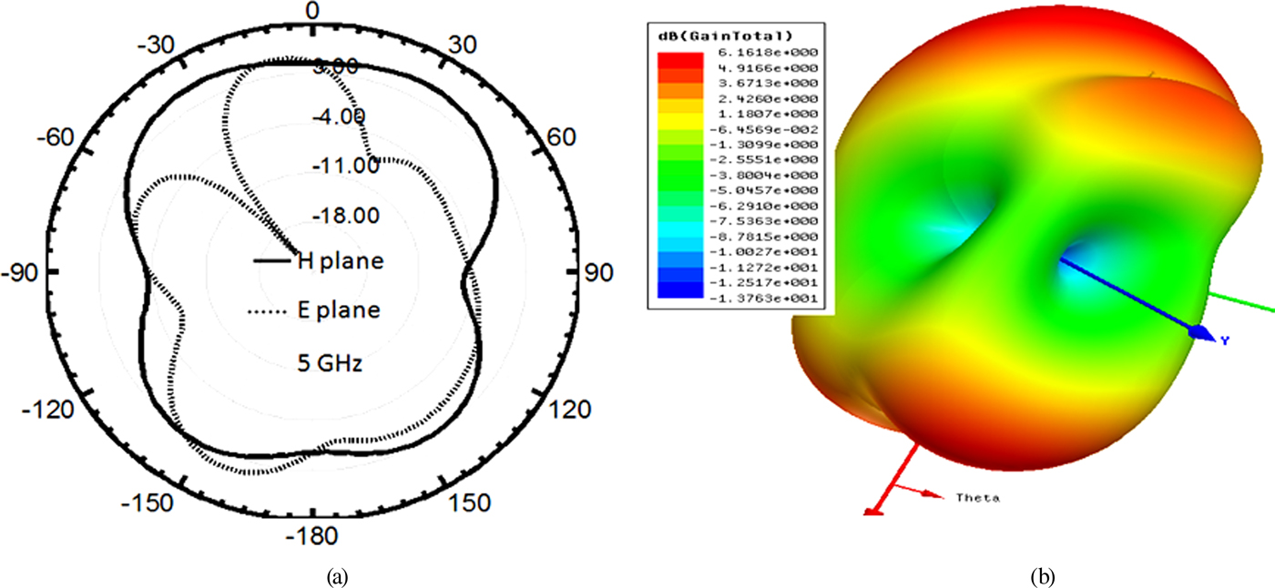
When integrated antenna is excited by port 1, it radiates signal from 2 to 11 GHz to identify the direction of maximum traffic or interference. Figure 14 shows that simulated and measured S 11 is better than −15 dB from 2 to 11 GHz and are in agreement with each other. The radiation pattern of UWB antenna is nearly omni-directional in E and H planes except a discontinuity at θ = 50° in E plane as shown in Fig. 15(a). The gain of antenna is 4 dB at 5 GHz; its 3D gain pattern is shown in Fig. 15(b).
S 11 versus frequency in spectrum-sensing mode.

(a) E and H planes, (b) 3D pattern for gain at 5 GHz.
B) Pattern reconfigurable mode
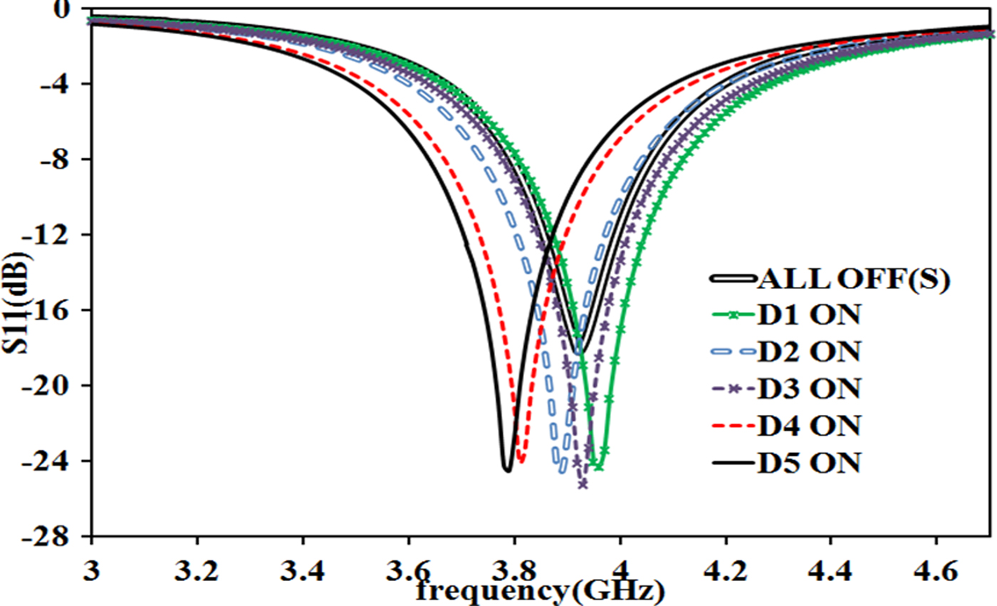
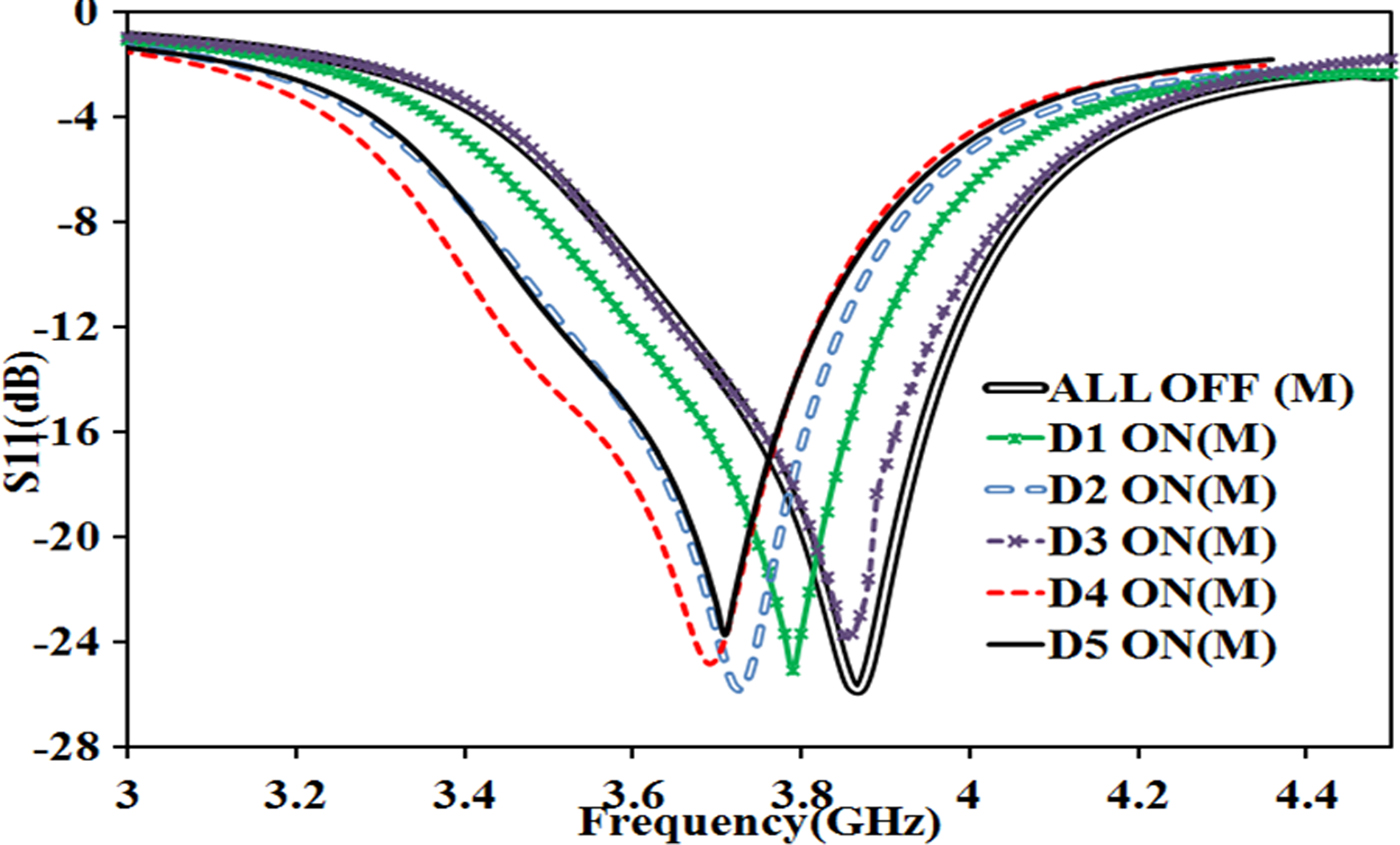
Here, pattern reconfiguration concept is verified experimentally. Six different cases are studied by controlling the different short position using diodes D 1 to D 5. Simulated and measured S 11 parameters for different shorting posts are given in Figs 16 and 17, respectively. The resonating frequency is nearly constant around 3.8 GHz for all the diode states with a bandwidth of nearly 170 MHz. RL for all the cases is better than 20 dB.
Simulated S 11 (dB) versus frequency for all cases.
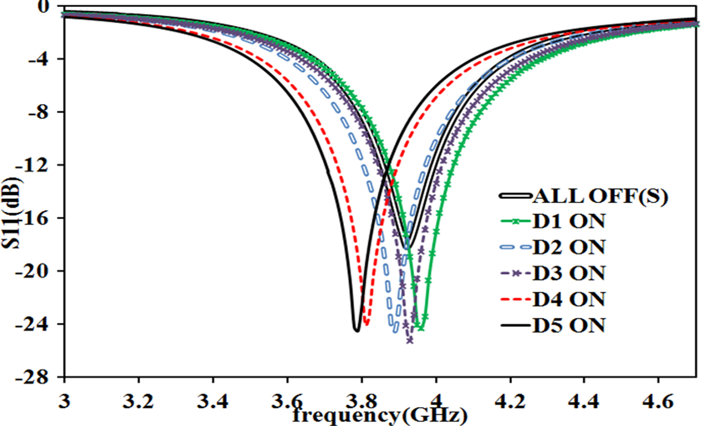
Measured S 11 (dB) versus frequency for all cases.
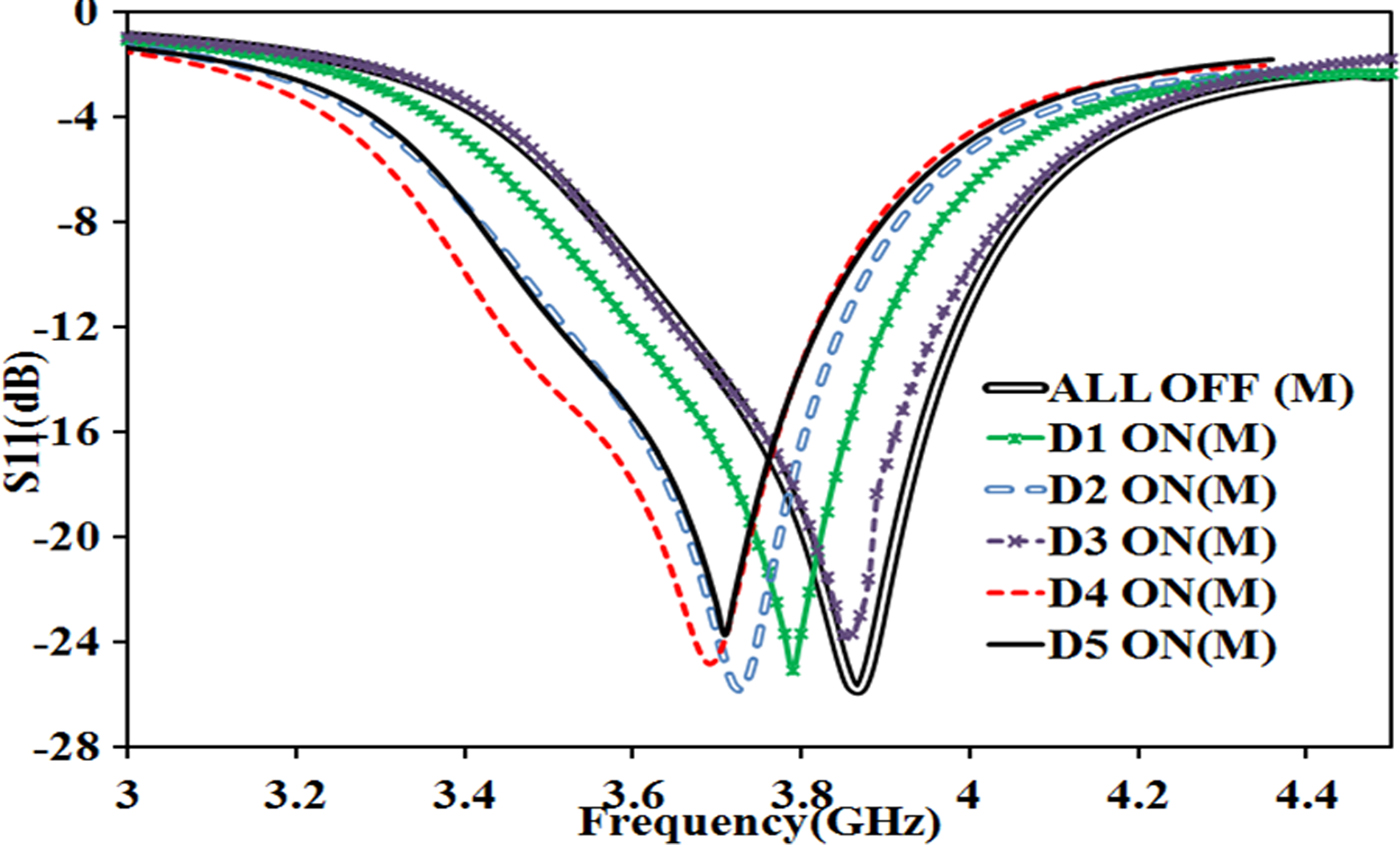
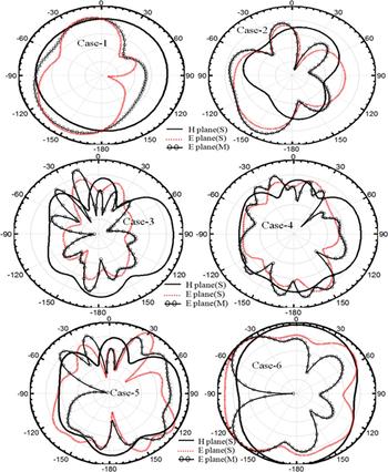
Figure 18 shows the E and H plane patterns for all the cases. In case 1, the antenna operates as a normal patch with no shorted post and it radiates its maximum intensity in 140° direction. The measured pattern is sighlty broader than the simulated one; however, maxiumum intensity is still pointed toward same direction as shown in Fig. 18(a). In case 2, when diode D 1 is ON, peak of the beam moves 10° away from its ideal value (case 1) as shown in Fig. 18(b). In this case, shape of pattern is changed to super cardioid having maximum radiation intensity pointed toward 150° direction. In case 3, when diode D 2 is shorted, observed E plane pattern is shown in Fig. 18(c). Simulated and measured radation patterns concide with each other. In this case, we observe multiple sidelobes in diferent elevation angles. These sidelobes can radiate some part of total energy, which is undesired for efficient radiation. In case 4, when diode D 3 is ON, to short the parasitic ring at 90°, the observed E plane pattern are shown in Fig. 18(d). Now the direction of main beam is observed nearly omni-directional in both planes. Both simulated and measured patterns show good agreement with each other. Figure 18(e) presents the E and H plane patterns for case 5 when diode D 4 is used to short the parasitic ring at 270°. For case 6, when parasitic ring is shorted at 315°, the main lobe redirected its total radiation intensity as shown in Fig. 18(f). The discrepancies between the simulation and measurement radiation patterns can be attributed to the presence of coaxial cables, connectors DC pads, lumped elements, and connecting wires for biasing different PIN diodes. These components are in close proximity to the antenna during the pattern measurements.
E and H plane patterns at 3.9 GHz.

C) Polarization reconfigurable mode
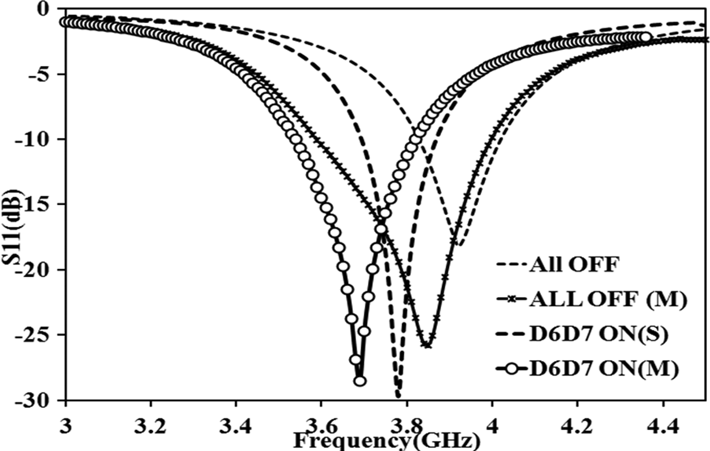
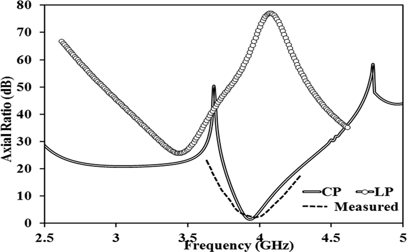
Polarization state of the proposed antenna can be changed by changing state of PIN diodes D 6 and D 7. Antenna has CP when both diodes (D 6, D 7) are kept OFF, i.e. no voltage is applied at bias pad V 6. Whereas, to achieve LP, both the diodes should be forward biased. Figure 19 shows the simulated and measured S 11 for both polarization states. From Fig. 19 one can see that when both diodes are OFF, then simulated value of RL = 19 dB at 3.9 GHz, whereas, measured value of RL = 25 dB at 3.83 GHz. When both diodes are ON, then antenna resonant at 3.78 GHz with RL = 30 dB as compared with measured resonant frequency of 3.7 GHz with RL = 29 dB. Figure 19 also show that 3 dB bandwidth of LP signal is much smaller compared with CP signal but still the 3 dB bandwidth of LP signal is 530 MHz, which is acceptable for any communication. The high value of 3 dB bandwidth for CP signal is attributed due to the presence of slots in the ground plane as well as in the patch area. But when both diodes D 6 and D 7 are turned ON, effective area of slot decreases which also reduces the bandwidth of the resonant signal. Figure 20 shows the simulated and measured axial ratio for both polarization states. The simulated value of axial ratio for CP is 1.6 dB at 3.9 GHz, whereas measured value of axial ratio is 1.7 dB at 3.9 GHz.
S 11 versus frequency in polarization reconfigurable mode.

Axial ratio versus frequency in polarization reconfigurable mode.

D) Frequency reconfigurable mode
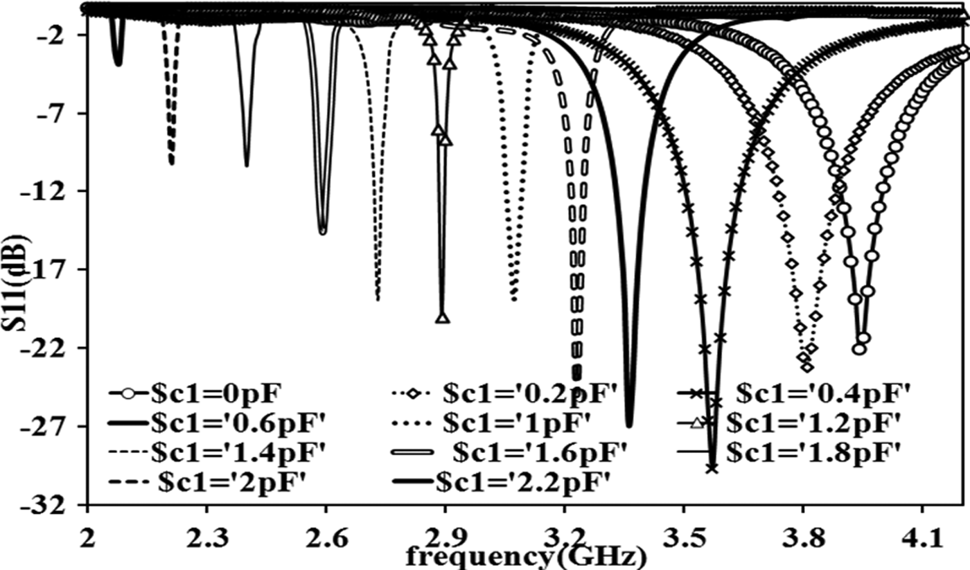
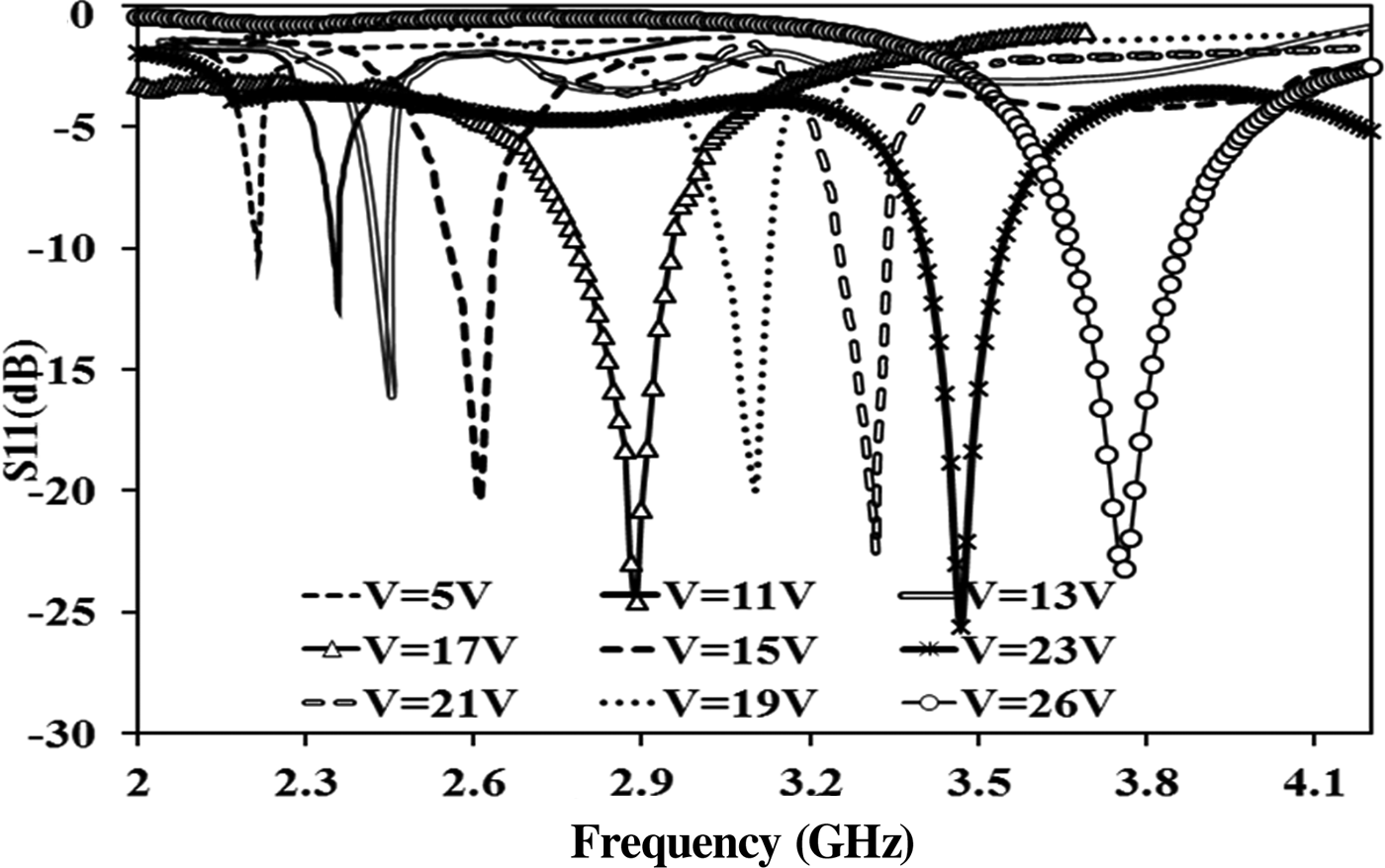
Frequency tuning is obtained by varying the reverse bias of varactor diode to provide various capacitive loadings across the slot. As different capacitive loadings of the varactor diode correspond to different electrical lengths, it corresponds to different resonant frequency. Figure 21 shows the parameter analysis in HFSS when capacitance is varied from 2.25 to 0.5 pF. The results clearly show that a continuous tuning of frequency ranging from 2 to 4 GHz is obtained. The reconfigurable antenna was then electronically tuned with a reverse DC voltage applied across the varactor diode. The variation of resonant frequencies with the applied reverse bias voltage is measured and plotted in Fig. 22. When the reverse bias is OFF, the varactor loading on the slot correspond to high capacitance (2.2–1.4 pF). Thus, the tuning range of resonant frequencies is lowered in band from 2.2 to 2.6 GHz with a frequency ratio of 1.18 when reverse bias is varied from 5 to 14 V. When the bias voltage is varied from 15 to 26 V, the varactor loading in the slot corresponds to low capacitance (1.4–0 pF). Thus, the tuning range for the resonant frequency is found from 2.6 to 4 GHz with a frequency ratio of 1.53. The simulated and measured results show that the obtained frequency response is quite narrow in nature. The narrow frequency response is mainly attributed to varactor diode which tunes the impedance bandwidth only in the short range of bandwidth.
Simulated S 11 versus frequency.

Measured S 11 versus frequency.

E) Bandwidth reconfigurable mode
In this mode, antenna can switch its operating bandwidth from NB to WB by switching the active port state. To obtain the NB response, integrated antenna is excited by port 2, and to obtain WB response, antenna is excited by port 1. In WB mode, active area of antenna is lower semicircular arc which radiates signal from 2 to 11 GHz with RL better than 15 dB. The simulated and measured results for this mode are shown in Fig. 14. In NB mode, active area of antenna is circular antenna which is excited by port 2. In this mode, various narrow frequency bands are obtained depending on reverse biasing the varactor diode. The frequency span in NB mode is 2–4 GHz, and simulated and measured results are shown in Figs 21 and 22.
The proposed integrated antenna is versatile in nature but highly compact in nature compared with versatile antenna proposed in [Reference Sharma and Tripathi11]. In this design, UWB antenna is integrated in electro inert area, whereas a separate UWB antenna is used in [Reference Sharma and Tripathi11] for spectrum sensing. In this proposed design, varactor diodes are used for continuous frequency tuning which gives narrow bandwidth and less frequency span over 2–4 GHz, whereas microstrip open stubs are used in [Reference Sharma and Tripathi11] which give discrete frequency tuning over a frequency span of 1.5–5 GHz.
V. CONCLUSION
A smart and reconfigurable antenna with smaller physical size meets the essential requirement for CR systems. Here, a versatile reconfigurable antenna capable of spectrum sensing along with various reconfiguration features is presented. The proposed antenna senses the spectrum by semicircular structure from 2 to 11 GHz to identify the spectrum conditions. In addition to spectrum sensing, this structure can be used as a wideband transmitting antenna. After recognizing the spectrum condition, the proposed antenna can reconfigure its polarization state, frequency, operating bandwidth as well as radiation pattern.
 Sonia Sharma received M.Sc. degree in Electronics Science from Maharishi Dayanand University, Rohtak in 2005. She received M.Tech. and Ph.D. degrees in Electronics and Communication Engineering from UIET, Kurukshetra University, Kurukshetra in 2011 and 2017, respectively. She has more than 15 research papers in various journals and conferences.
 Chandra Charu Tripathi received the B.Sc. and M.Sc. degrees from Banaras Hindu University, Varanasi, followed by M.Tech. degree in the year 1991 from BITS, Pilani, India. His research interest includes MEMS, thin film deposition, reconfigurable devices. He has published around 80 research papers in international/national journals of repute.
 Rahul Rishi received his Ph.D. from M. D. University, Rohtak, India in the year 2005. Ten research scholars have completed their doctoral work under him. He has published around 80 research papers in international journals of repute. His research interests include management of uncertainty through probabilistic databases, spatio-temporal databases, soft computing techniques, and cognitive radio.