Introduction
TiO2 is one of the most prominent material known in performing various kinds of functions in many areas including photocatalytic water splitting for hydrogen production [Reference Qi, Cheng, Yu and Ho1, Reference Wen, Li, Liu, Fang, Xie and Xu2], organic pollutant degradation [Reference Wu, Liu, Qiu, Li, Zhou, Fang, Zhang and Li3, Reference Wu, Li, Liu and Zhang4], photovoltaic cells [Reference D’Souza, Muralikrishna, Chandan, Ramakrishnappa and Balakrishna5, Reference Lee, Raga, Yuichi, Leyden, Ono, Wang and Qi6], lithium-ion battery [Reference Liu, Tian, Tan, Li and Chen7, Reference Yan, Tian and Chen8], and supercapacitors [Reference Liu and Chen9]. TiO2 is the most preferred photoanode used in dye-sensitized solar cells (DSSCs) [Reference Xu, Wang, Fan, Liu, Cao and Yu10, Reference Miao, Pan, Liao, Zhou, Pan and Wang11]. Since the pioneering work of O’Regan and Grätzel in 1991, the DSSCs have attracted extensive attention from both scientific and technological aspects because of their intrinsic advantages of easy production, nonpolluting, low cost, and relatively high-power conversion efficiency (η) [Reference Wang, Zakeeruddin, Moser, Nazeeruddion, Sekiguchi and Grätzel12, Reference Bai, Cao, Zhang, Wang, Li, Wang, Zakeeruddion and Grätzel13, Reference Manju and Jawhar14]. Typically, the photoanode of a DSSC is made of a TiO2 nanoparticle (NP) mesoporous film on transparent conductive oxide glass, and a monolayer of a ruthenium-based complex dye is usually absorbed to its surface. Up to now, photoanodes in high-performance devices are composed of nanoporous anatase TiO2 NPs because of their large surface area [Reference Pan, Zhou, Tian, Pan, Tian, Xie, Dong, Wang and Fu15, Reference Chen, Wang, Li, Pootrakulchote, Alibabaei, Ngocle, Decoppet, Tsai, Grätzel, Wu, Zakeeruddin and Grätzel16]. However, there are numerous grain boundaries in TiO2 NPs, which limit the η of DSSCs. Their performance is impaired by poor electron transport, too many surface traps, repeated charge recombination, and low light scattering capabilities [Reference Park, Zhang, Myers and Cao17, Reference Roy, Kim, Lee, Spiecker and Schmuki18].
To overcome this limitation, recent researches have been directed toward the use of one-dimensional (1D) TiO2 nanostructures, such as nanotubes (NTs) [Reference Akilavasan, Wijeratne, Moutinho, Al-Jassim, Alamoud, Rajapakse and Bandara19, Reference Barai, Banerjee, Bai and Joo20], nanorods (NRs) [Reference Liu and Aydil21, Reference Zhang, Wang, Liu and Li22], and nanowires (NWs) [Reference Ling, Song, Chen, Yang, Qiao and Du23, Reference Riaz, Qi, Fang, Xu, Zhou, Jin, Hong, Zhi and Liu24]. These 1D nanostructures with high crystallinity can provide direct pathways for photogenerated electrons and decrease intercrystalline contacts and thus significantly suppress the charge recombination characteristics [Reference Zhu, Neale, Miedaner and Frank25, Reference Qiao, Liu, Huang, Lei, Sun and Sun26]. Additionally, the light trapping effect becomes more significant with increased packing density and aspect ratio of 1D nanostructures, which leads to speculation regarding the influence of the morphology on the light absorption [Reference Mathew, Rao and Munichandraiah27]. Unfortunately, the specific surface area of the high crystallinity 1D nanostructures is much lower than that of TiO2 NP porous films. So, they cannot anchor enough dye molecules on surfaces to produce more photogenerated electrons. The photocurrent output and the η of simple 1D nanostructure-based DSSCs are inferior to those of conventional TiO2 NP porous films [Reference Liu, Huo, Zhang and Dong28, Reference Hu, Shen, Cao, Wang, Lv, Zhang, Zhu, Zhao and Cui29].
As discussed above, the combination of high surface area and fast electron transport with excellent light-harvesting efficiency is essential for an ideal photoanode material. Recently, hierarchical 1D nanostructures, such as branched NRs, NWs, and NTs, were synthesized and are proved to be novel materials [Reference Pan, Dong, Zhou, Wang, Pan, Yuan, Miao and Tian30, Reference Yuan, Chen, Zou and Wang31, Reference Liu, Su, Zhang, Wang, Yang, Shen, Deng, Zhang and Zhang32]. Fu et al. fabricated TiO2 NW-NP/NT architecture for DSSC, which exhibits a doubled conversion efficiency of 8.21% compared with DSSC based on pristine TiO2 NTs [Reference Fu, Liu, Liu, Lu, Zhou, Peng and Huang33]. Gao et al. prepared DSSCs based on ZnO NR/NP structure; the power conversion efficiency increased from 1.35 to 3.63% with 169% enhancement as compared to that based on ZnO NR [Reference Gao, Cui, Liu, Wang and Cao34]. Previous studies on the effect of hierarchical nanostructure focused on structural design. Few researches focused on the interface connection between the functions layers of photoanode (e.g., transparent conducting glass/TiO2/dye film interface [Reference Zeng, Ni, Su, Chen and Jiang35]), even though the corresponding works revealed that through enhancing interface connection, electron lifetime could be lengthened and the electron transport time could be shortened, as electrons could move more smoothly to external circuit [Reference Fu, Liu, Liu, Lu, Zhou, Peng and Huang33, Reference Gao, Cui, Liu, Wang and Cao34, Reference Zeng, Ni, Su, Chen and Jiang35]. Moreover, the most widely used configuration of photoanode is still in a bilayer structure [Reference Fu, Liu, Liu, Lu, Zhou, Peng and Huang33]. However, most works on scattering layers have not involved the interface connection between the top scattering layer and bottom layer.
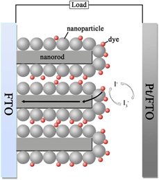
Herein, a TiO2 NP/NR array hierarchical nanostructure termed as TiO2 NP/NR is fabricated and applied as photoanode of DSSCs, designed as showed in Scheme 1. A systematic investigation revealing the effects of TiO2 NP/NR composite on the performance of DSSCs is conducted in comparison to the TiO2 nanorod (TiO2 NR) arrays and TiO2 nanoparticles (TiO2 NRs). Based on our results, the TiO2 NP/NR nanostructure possesses superior performance, such as large surface area, efficient light scattering, and fast electron transport, which are beneficial for the photovoltaic performance of DSSCs. The underlying interfacial electron transmission mechanisms for the enhanced photovoltaic performance have been studied in detail. However, we found that many factors limit the further improvement of the photoconversion performance of TiO2 NP/NR-based DSSC during the research. Therefore, further work is needed to address these issues.
Scheme shows nanostructure of NP/NR-based DSSC and electron transport mechanism in the photoanode.

Results and discussion
Morphology and structure of TiO2 NR and TiO2 NP/NR composites
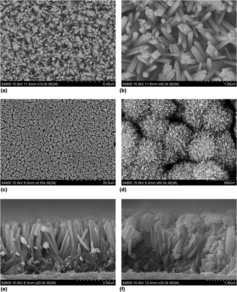
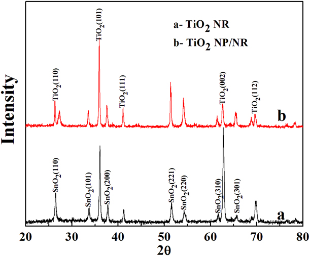
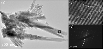
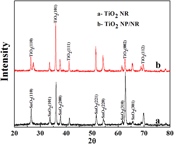
The TiO2 NR grown on FTO by hydrothermal reaction has a preferential orientation. It is distributed uniformly and densely over the entire surface of the FTO substrate [Fig. 1(a)]. The shape of the NRs is tetragonal with square top facets and smooth side surfaces, which is a negative factor for dye adsorption. The width of the NRs is between 100 and 200 nm, and the length is about 3 μm [as shown in Fig. 1(b) and Fig. 1(e)]. The XRD pattern of the TiO2 NR on the FTO substrate [Fig. 2(a)] shows that the diffraction peaks of TiO2 NR agree well with the tetragonal phase of the rutile TiO2 (refer to ICDD-PDF No. 01-088-1175), which is consistent with the previous report [Reference Liu and Aydil21]. Only (101) and (002) peaks exist in the XRD spectrum, and the (002) peak is enhanced significantly, which indicates that the NR is probably single crystalline. A typical TEM image of TiO2 NRs is shown in Fig. 3(a). It reveals that the nanorod’s surface is smooth, and their average diameter is about 200 nm. The sharp two-dimensional lattice image [Fig. 3(b)] and SAED pattern [Fig. 3(c)] confirm that the NR is crystalline. Its ordered crystalline structure and two d-spacing values about 3.24 and 2.93 Å are observed, which are consistent with the lattice distances of (110) and (001) planes of TiO2 rutile phase, respectively. The NRs grow along the [001] direction and have the (002) facets exposed on top, which agree well with the XRD data.
(a) Low magnification and (b) high magnification EFSEM images of the TiO2 nanorod arrays; (c) low magnification and (d) high magnification EFSEM images of the TiO2 NP/NR composites; (e) cross-sectional image of TiO2 nanorod arrays; (f) cross-sectional image of TiO2 NP/NR composites.

XRD patterns of TiO2 NR (a) and TiO2 NP/NR (b) after sintering at 450 °C for 30 min.
(a) Typical TEM image of the TiO2 NR; (b) HRTEM image of NR; (c) the corresponding selected area electron diffraction (SAED) pattern in (a).

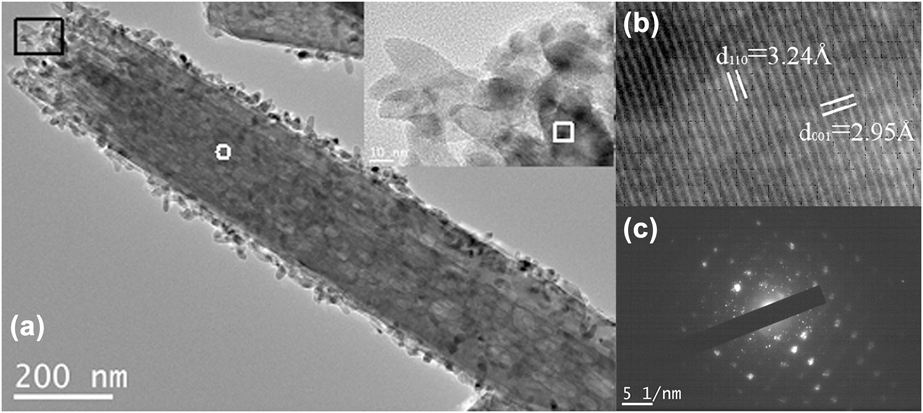
Using TiO2 NR substrate, the NPs form on the TiO2 NRs after a simple wet chemical route for 24 h. As shown in Figs. 1(c), 1(d), and 1(f), the NPs uniformly grow on TiO2 NRs and fill in the interstices of the NR arrays. It is expected that the NPs can significantly improve the specific surface area and roughness of the TiO2 NR. The XRD patterns of the TiO2 NP/NR composites are displayed in Fig. 2(b). The crystal structures of TiO2 NP/NR composites are rutile phase, which shows that the crystal structure of the TiO2 NPs is rutile. Compared with the TiO2 NR, the relative intensity of the (002) peak of the TiO2 NP/NR composites is weak and the other diffraction peaks are enhanced, such as (110), (211), and (112), which could be attributed to the large number of unordered TiO2 NPs around the oriented NRs. TEM image of the TiO2 NP/NR composites [Fig. 4(a)] demonstrates that the NR is uniformly covered by TiO2 NPs, and its surface roughness increases compared with the simple TiO2 NR in Fig. 3(a). The inset in Fig. 4(a) shows the nanoparticles on the top of the NR, whose diameters are in the range of 15–25 nm. Figure 4(b) shows a HRTEM image of one TiO2 NP, and the interplanar spacings of 3.24 and 2.93 Å confirms rutile phase for the NP. TiO2 NP is also single phase. The formation of rutile phase NPs is due to the presence of Cl−. Cl− can reduce the surface energy of the crystal plane side wall, promoting anisotropic growth in the [001] direction [Reference Yang, Sun, Qiao, Zou, Liu, Smith, Chen and Lu36]. Figure 4(c) is SAED pattern of TiO2 NP/NR composites. The lattice fringe of the NP is not aligned to the single-crystal NR, indicating that there is no epitaxial relationship between NRs and NPs. The results of the TEM and HRTEM are consistent with the XRD and FESEM data.
(a) Typical TEM image of TiO2 NP/NR composites, the inset is TEM image of NPs on the top of NR; (b) HRTEM image of the NP on the NR; (c) typical SAED patterns of the TiO2 NP/NR composites.

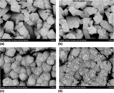
The effect of growth time on TiO2 nanoparticles is investigated through the surface morphology of TiO2 NRs immersed in TiCl4 aqueous solution for different time as presented in Fig. 5. There are numerous tiny buds grown on the surface of NRs when the reaction time is 6 h [Fig. 5(a)]. After 15 h, the tiny buds grow to NPs, but there is no significant changes in the overall morphology [Fig. 5(b)]. Up to 24 h, the morphology of nanostructures becomes conspicuous [Fig. 5(c)], which indicates that the growth rate of NPs is faster than that in the early period of the synthesis. As shown in Fig. 5(d), when the reaction time prolonged to 33 h, the NPs interconnected with one another and filled the gaps along the NRs. The above growth rate variations are due to the complexity of TiCl4 cryogenic hydrolysis. In the hydrolysis process of Ti4+ in aqueous solution, it is difficult to exist in solution in the form of simple ions because of its small radius, but forms complex complexes with water. Driven by oversaturation or undercooling, complex complexes further aggregate to form complex polynuclear complex complexes with the same crystal structure as the solid phase. These complex complexes are considered to be embryos. These embryos grow by absorbing the solute in the solution, forming a crystal nucleus with a certain critical size, and then developing into a complete crystal. The whole process of crystallization is the process of forming and growing crystal nucleus. With the extension of time, the hydrated titanium dioxide particles with agglomeration gradually precipitated down. At this stage, as the equilibrium of hydrolysis in the solution is broken, the hydrolysis speed is increased. The titanium dioxide component in the liquid phase is transferred to the hydrated titanium dioxide precipitation in the solid phase. The concentration of Ti4+ in the solution keeps decreasing and the concentration of free acid rises sharply [Reference Liveri37].
The FESEM images of TiO2 NRs treated by an aqueous of 0.2 M solution TiCl4 at 30 °C for different times: (a) 6 h, (b) 15 h, (c) 24 h, and (d) 33 h.

Optical and dye adsorption properties
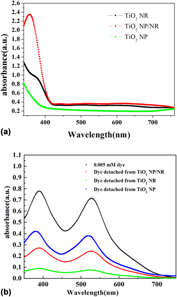
To evaluate the optical properties, the UV-vis absorption spectra of the TiO2 NP, TiO2 NR, and TiO2 NP/NR measured from 300 to 800 nm are compared in Fig. 6(a). It can be found that TiO2 NR and TiO2 NP/NR have excellent light absorption than TiO2 NP, and the absorbance of TiO2 NP/NR is higher than that of TiO2 NR in visible region. The red shift of the absorption wavelength occurs for TiO2 NRs and NP/NR. The final formed TiO2 NPs in hierarchical nanostructure expands the red-shift extent for TiO2 NP/NR. [Reference Song, Li and Wang38, Reference Shi, Guo, Liu, Su and Guo39]. It indicates that the light harvesting efficiency of TiO2 NP/NR composites is better than the pure TiO2 NR and TiO2 NP. It can be concluded that the loaded TiO2 NPs could enhance light absorption and thus probably improve the photovoltaic properties of the DSSC.
(a) The UV-vis absorbance spectra of TiO2 NP, TiO2 NR, and TiO2 NP/NR films; (b) UV-vis absorptions of solutions containing 0.005 mM N719 dye and dyes detached from the TiO2 NP, TiO2 NR, and TiO2 NP/NR films.

The increased adsorption amount of the dye in the electrode composed of TiO2 NP/NR composite can be testified by the dye absorption experiments [Reference Liu and Aydil21]. Figure 6(b) shows the absorption spectra of the solutions containing 0.005 mM dye and dye detached from the TiO2 NR and TiO2 NP/NR composite electrodes (1 cm2 area for both) in 20 mL of ethanol containing 0.1 mM KOH. The dye loading amount is calculated using Lambert–Beer law [Reference Nazeeruddin, Zazeeruddin, Humphry-Baker, Jirousek, Liska, Vlachopoulos, Shklover, Fischer and Grätzel40],
 $$A = \varepsilon bc\quad ,$$
where A is absorbance, ε is extinction coefficient, b is width of curette, and c is solution concentration. Extinction coefficient, ε, is constant for dye, and the value of b is fixed. Absorbance, A, is thus proportional to concentration, c. Using the 0.005 mM dye solution as a reference, the dye loading amount for the TiO2 NR and TiO2 NP/NR electrodes is calculated to be 1.05 × 10⁻⁸ and 3.40 × 10⁻⁸ mol/cm2, respectively. The loading amount of the latter is about three times higher than that of the former. Such high loading amount may lead to a higher short circuit current density and therefore higher photovoltaic conversion efficiency. However, the dye loading amount of TiO2 NP/NR electrode is still lower than that of the electrode (5.66 × 10⁻⁸ mol/cm2) based on TiO2 NPs.
The specific surface areas and pore structures are of great importance for the energy conversion efficiency of DSSCs. Therefore, BET surface areas and pore structures of the samples were investigated by the N2 adsorption–desorption measurement. The specific BET surface areas of TiO2 NP/NR and TiO2 NP are 52.14 m2/g and 83.58 m2/g. Figure S1 shows N2 adsorption–desorption isotherms of TiO2 NP/NR and TiO2 NP powders scraped from photoanodes. The adsorption isotherms of both of the samples were of type IV, indicating the presence of mesopores (2–50 nm) according to BDDT (Brunauer–Deming–Deming–Teller) classification [Reference Yu, Yu, Leung, Ho, Cheng, Zhang and Zhang41]. The shape of hysteresis loops for the sample TiO2 NP was of type H3 at high relative pressure between 0.8 and 1.0, associated with the presence of slit-like pores [Reference Yu, Yu, Cheng, Hark and Lu42]. The high adsorption capacity of the TiO2 NP at high relative pressure (P/P 0) range (approaching 1.0) demonstrated the existence of large mesopores and macropores. On the other hand, the shape of the TiO2 NP/NR has two hysteresis loops. At low relative pressures between 0.4 and 0.8, the hysteresis loops are of type H2, which can be observed in the pores with narrow necks and wider bodies (ink-bottle pores) [Reference Yu, Yu, Cheng, Hark and Lu42]. However, at high relative pressures between 0.8 and 1.0, the shape of the hysteresis loop is of a type H3, associated with NP/NR particles giving rise to narrow slit-shaped pores [Reference Yu, Yu, Cheng, Hark and Lu42]. The results were further confirmed by the corresponding pore-size distribution (Fig. S1) calculated by the BJH method from adsorption isotherm. The pore-size distribution curves of the TiO2 NP show big mesopores with diameters of approximately 40 nm, which were formed between stacked NPs. The TiO2 NP/NR showed bimodal pore-size distribution with the micropores (diameters about 2 nm) and the mesopores (diameters about 13 nm). This bimodal pore-size distribution was ascribed to fine intra-aggregated pore within the deposited particles on the TiO2 NR and large inter-aggregated pore between the TiO2 NP/NR. The macroporous structure of TiO2 NP/NR could be directly observed from the SEM images of the TiO2 NP/NR displayed in Fig. 1(d). Although the TiO2 NP/NR has lower BET surface areas than the TiO2 NP, the large mesopore in several tens to several hundred nanometers in TiO2 NP/NR can enhance the absorption of light and provide efficient transport pathways for electrolyte molecules.
Effect of TiO2 NP/NR composites on the photovoltaic performance
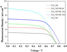
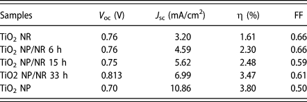
The photocurrent density–voltage curves of the various DSSCs are shown in Fig. 7, and the corresponding photovoltaic parameters are summarized in Table I. As is indicated, the 3 μm long TiO2 NR-based DSSC exhibits an open-circuit voltage (V oc) of 0.76 V, a short-circuit current (J sc) of 3.20 mA/cm2, a fill factor (FF) of 0.66, and an overall efficiency (η) of 1.61%, which are lower than that of the 5 μm long TiO2 NP-based DSSC (V oc, J sc, and FF values of 0.70 V, 10.86 mA/cm2, and 0.50, η = 3.8%, respectively). This can be attributed to the low specific surface area and high crystallinity of TiO2 NR resulting in the reduction of dye adsorption, which in turn leads to the low J sc. However, compared with the dye loading capacity of the NR film, which is only 18.6% of that of NP film, the J sc and the η of the NR cell are still remarkable. Meanwhile, the filling factor (FF = 0.66) of the NR DSSC is superior to the NPs (FF = 0.50). It may be attributed to the synergistic effect of efficient light scattering for sufficient light harvesting and fast charge transport for efficient charge collection in the TiO2 NR photoanode.
Photocurrent–voltage characteristics of the DSSCs based on TiO2 NP/NR with different reaction time, TiO2 NP, and TiO2 NR.

DSSCs performance from the J–V characteristics based on TiO2 NR/NP for different reaction times.

For a series of TiO2 NP/NR-based DSSCs, the J sc gradually increases with the nucleation and growth of the NPs on the NRs, whereas the V oc is increased and FF is slightly reduced. The TiO2 NP/NR 33 h-based DSSC exhibits V oc, J sc, and FF values of 0.813 V, 6.99 mA/cm2, and 0.61%, respectively, along with the best η of 3.47%, which is about 2.2 times the efficiency obtained with the TiO2 NR device. The enhanced performance of TiO2 NP/NR 33 h-based DSSC is mainly attributed to 2.18-fold increase of photocurrent output (from 3.20 to 6.99 mA/cm2), which is consistent with the result of dye adsorption amount. Unsurprisingly, the η (3.48%) of 3 μm long TiO2 NP/NR 33 h-based DSSC rivals that of 5 μm long P25-based DSSC (3.80%), although the dye adsorption amount of 5 μm long P25 photoanode is more than 3 μm long TiO2 NP/NR photoanode. What’s more, the V oc and FF of the TiO2 NP/NR-based DSSCs are superior to the P25. The 3 μm long TiO2 NP/NR-based DSSC shows excellent photoelectric conversion performance. This can be attributed to the following reasons. First, highly crystallized TiO2 NP/NR composites have fewer defects on the surface, such as vacancy, dangling bonds, or microvoids, which is beneficial to reduce probability of the recombination of photogenerated electrons and holes. Second, according to the test results of SEM and BET, the pore volume of TiO2 NP/NR films is larger than that of P25 film, which can enhance transfer, and diffusion of I3−/I− to regenerate the dye is important to the photovoltaic response of the solar cells. Third, the synergistic effect of the light trapping effect in TiO2 NR and high specific surface area for dye absorption in TiO2 NPs result in a significant increase in the light harvesting capability of the photoanode.
Transport and recombination properties of photoanode
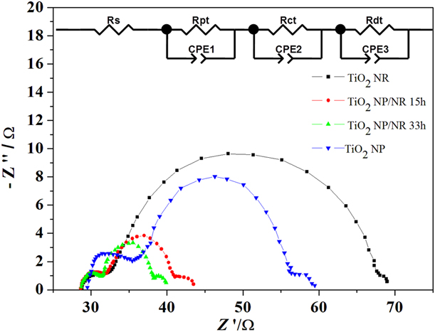
The EIS is one of the most powerful method to investigate internal resistances for the charge transfer process of DSSCs [Reference Gao, Xu, Bai and Jin43, Reference Qi, Yin, Zhang, Ouyang, Li and Chen44, Reference Zhang, Pan, Zhou, Yu, Pan, Jiang, Tian, Wang, Xie, Dong, Miao and Tian45]. As shown in Fig. 8, the typical Nyquist plots of the DSSCs under 1.0 sun illumination are measured at open-circuit potential. For the analysis of the spectroscopic data, an equivalent circuit for DSSCs (inset in Fig. 8) is employed [Reference Llaiyaraja, Das, Mocherla and Sudakar46]. Typically, the starting points for all of the spectra resemble the R s, which represent the contact impedance between FTO substrate and the metal ohmic contact. Then, from high to low frequency, the three semicircles in the Nyquist impedance spectra are observed. The impedance at high frequency (1 k–100 kHz) in the impedance spectra corresponds to the capacitance and charge transfer resistance (R Pt) at the platinum counter electrode/electrolyte interface. The medium-frequency response at 1–1 kHz is associated with the charge transfer resistance (R ct) in the nanocrystalline TiO2/dye/electrolyte interface. The large semicircle in the lower frequency region corresponds to the electrolyte ion diffusion of I−/I3− redox electrolytes [Reference Qi, Yin, Zhang, Ouyang, Li and Chen44]. The C PE is constant phase element in the cells.
EIS spectra of DSSCs based on TiO2 NR, TiO2 NP, and TiO2 NP/NR. The inset is equivalent circuit of the DSSC.

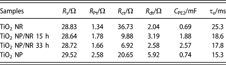
The resultant values of R s, R Pt, R ct, R dt, and C PE2 fitted by ZView software using the equivalent circuit are shown in more details in Table II. It is obvious that the R s and R Pt have almost no differences, which is verified that the substrate of photoanodes and the counter electrode/electrolyte interface are the same. Compared with the NP photoanode, the R s values of NR and NP/NR photoanodes are slightly lower. This is because the roots of nanorods are closely arranged on the FTO substrate (Fig. 1), avoiding contact resistance between the substrate and the electrolyte. For diffusion resistance of I−/I3− in the electrolyte (R dt), TiO2 NP assembly DSSC exhibits highest value. This is attributed to that the pore volume of TiO2 NR and NP/NR films (Fig. 1) are larger than that of P25 film, which can enhance transfer and diffusion of I3−/I−. Meanwhile, TiO2 NP porous film provides narrow and tortuous channels, which inhibit the diffusion of I−/I3−. Thus, TiO2 NP has the highest value of the R dt.
Various impedance values estimated from the Nyquist impedance plots.

Here we focused on the comparison of R ct because a lower interface resistance will result in faster interfacial electron transfer, which favors a higher η. The fitting value of R ct is 36.73 Ω for TiO2 NR, 9.88 Ω for TiO2 NP/NR 15 h, 6.92 Ω for TiO2 NP/NR 33 h, and 20.65 Ω for TiO2 NP, respectively. Among them, the TiO2 NR photoanode has highest charge transfer resistance (R ct) in photoanode/dye/electrolyte interface, which due to the TiO2 NR with larger diameter (200 nm) and inefficient interact surface corresponded to larger interfacial resistance and higher current loss. Nevertheless, compared with NR-based DSSC, the NP/NR-based DSSCs show the less charge transfer resistance at the TiO2/dye/electrolyte interface and thus the higher η. This may be because the TiO2 NP optimized the contact in transmission interface. The 20 nm NPs have a higher quantum size effect compared with NRs with 200 nm in diameter. Therefore, the NPs have better electron gain and loss capability, improving the interpenetration of electrolyte [Reference Qu, Li and Gao47]. Meanwhile, the TiO2 NRs promoted the photogenerated charge transfer and decreased the charge recombination rate. This clearly implicates the facilitation of efficient electron injection and transport in composite photoanode. The R ct values of NR/NP composite photoanodes are lower than the NP photoanode. It suggests that the NR/NP photoanode improves the defect of electron transport in NPs, which is large back electron transfer caused by grain boundaries and lattice defects. The lower R ct value benefits a potential DSSC and results in larger FF and V oc values, thus leading to enhancement in overall cell efficiency. These results are in accordance with the photoelectrical conversion efficiency data discussed above.
The electron lifetime τe is calculated by the following formula [Reference Lin, Lin, Lee and Chen-Yang48]:
 $${\tau _{\rm{e}}} = {R_{{\rm{ct}}}} \times {C_{{\rm{PE2}}}}\quad .$$
The electron lifetime τe of various photoanodes is calculated to be 25.3 ms, 18.6 ms, 17.8 ms, and 15.3 ms for NR, NR/NP and NP, respectively. The shortest lifetime in TiO2 NPs reflects a highest electron recombination rate during the electrons transfer across grain boundaries. However, the NR DSSC has longest electron lifetime, because the TiO2 NRs with high crystallinity can offer a direct conduction pathway and fast electron transport. For the TiO2 NP/NR photoanode, the electron lifetime falls between those in TiO2 NR and TiO2 NP photoanode, suggesting that the NPs increase the transmission time of the injected electrons in grain boundaries. After loading TiO2 NPs, the TiO2 NP/NR electrode can enhance the dye loading and light harvesting and greatly reduce series resistance, which could compensate the reduction of electron lifetime. Therefore, the overall conversion efficiency is improved.
PL spectra is conducted to confirm the effect of separation of photogenerated electron–hole pairs (Fig. S3). The peak centered at around 550 nm is attributed to the relaxation of self-trapped excitons, and the difference between peak intensities was the result of different electron–hole recombination rate of excited electrons in TiO2 structure. The intensity in TiO2 is the smallest, which is most likely due to the high crystallinity and superior transmission path of TiO2 NR, thereby depressing the recombination process. TiO2 NP/NR displays dramatically diminished PL intensity as compared with TiO2 NP, suggesting that recombination of photogenerated electron–hole pairs in TiO2 NP/NR is efficiently suppressed. This is due to TiO2 playing the role of electron capturers. Consequently, easier electron transfer activities are expected. These results are in well accordance with EIS and photoelectric conversion performances.
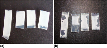
Above all, the results in this article confirm the NR/NP photoanode with higher levels of dye loading and light harvesting as well as efficiency of the DSSC. But the NR/NP photoanode has its limits. It is noted that the η value of the DSSCs based on NR/NP is much lower than that of the previously reported conventional DSSCs based on TiO2 NPs film [Reference Bai, Cao, Zhang, Wang, Li, Wang, Zakeeruddion and Grätzel13]. This is mainly attributed to the much smaller thickness (3 μm) of NR/NP film, which greatly limits the dye loading and hence limits the light harvesting. The NR array grown on the FTO substrate is inclined and may form intersections between the NRs, which stops the growth of NR (Fig. 1). Meanwhile, the NR film on the FTO substrate could fall off the substrate in our experiment, if NRs stay in the reaction solution for more than 48 h, as shown in Fig. 9. In the previous literature, the rutile phase TiO2 is disadvantageous in electron transport [Reference Grätzel49], but the phase of the NRs and NPs in our experiment is rutile, which is bound to affect the performance of the DSSC. The following work can be conducted from the three aspects: first, constructing sufficiently long vertically-ordered nanoarrays improves the performance of the light harvesting. Second, effective combination of the film and the substrate should be ensured. Third, fabricate rutile/anatase or anatase/anatase hierarchical nanostructure.
(a) Perfect TiO2 NR array film; (b) detached TiO2 NR array film.

Conclusions
In summary, the hierarchical TiO2 NP/NR composites were synthesized by a two-step hydrothermal reaction on FTO substrates and the power conversion efficiency of DSSCs can be successfully optimized by enhancing both open-circuit photovoltages and short-circuit photocurrent densities compared to the TiO2 NR and TiO2 NP. The power conversion efficiency of TiO2 NP/NR-based DSSC is 2.2 times higher than the NR-based DSSC. To obtain similar energy conversion efficiency, the amount of adsorbed dye of the modified TiO2 NP/NR-based DSSCs is far less than that of TiO2 NP-based DSSCs. This is because the TiO2 NP/NR photoanodes have large surface area and exhibit excellent light scattering, allowing for fast interfacial charge transfer and less charge recombination. The research provides a potential approach to obtain highly effective solar conversion materials. However, further work is needed to overcome the limitations of TiO2 NP/NR and improve the performance of TiO2 NP/NR-based DSSC.
Experimental section
Materials
All reagents are analytical grade without further purification. Titanium tetrachloride, tetrabutyl titanate, hydrochloric acid (by weigh 36–38%), and terpineol are obtained from Sinopharm Chemical Reagent Co., Ltd. (Shanghai, China). FTO conducting glass (fluorine-doped SnO2, resistance 15 Ω/square, transmittance 90%) was received from Nippon Sheet Glass Co., Ltd. (Itami, Japan). N-719 dye is purchased from Dyesol Ltd., Queanbeyan, Australia. Acetonitrile, iodine (purity of 99.9%), lithium iodide hydrate (99.99%), 4-tert-butylpyridine (TBP, 99%), and hydrogen hexachloroplatinate (IV) hydrate (H2PtCl6) are from Aldrich. 1-Methyl-3-propylimidazolium iodide (MPII), Surlyn 1702 film, and TiO2 (P25, 20–30 nm) are purchased from Dalian Rainbow Solar Technology Development Co., Ltd., Dalian, China.
Synthesis of TiO2 NP/NR composites
TiO2 NP/NR composites are grown on FTO substrates using a wet chemical route. In a typical synthesis, TiO2 NRs are first hydrothermally grown on FTO substrates in 60 mL of an aqueous hydrochloric acid solution (the ratio of deionized water to HCl is 1:1) and 1 mL tetrabutyl titanate at 160 °C for 18 h according to the reported method [Reference Liu and Aydil21]. Then, the obtained FTO substrates are immersed in 0.2 M TiCl4 aqueous solution and are kept at 30 °C for 6, 15, 24, and 33 h in a beaker covered with parafilm to prepare TiO2 NP/NR composites. The product is then rinsed with ethanol and dried in the air.
DSSC preparation
Dye-sensitized solar cells are assembled using TiO2 NR, NP/NR, and NP as the photoanodes, respectively. N-719 dye is used to sensitize the TiO2-based electrodes. In detail, the photoanodes made from TiO2 NR or NP/NR composites are first annealed at 450 °C for 30 min before the dye soaking process. Dye adsorption is performed by immersing the photoanodes in 3 × 10⁻⁴ M ethanol solution of N-719 at room temperature for 24 h. Then the electrodes are rinsed in ethanol. A sensitized electrode and a platinized FTO counter electrode are sandwiched together with a thermoplastic frame (Surlyn, 25-μm thick) to form a cell. The redox electrolyte solution containing 0.5 M MPII (1-methyl 3-propylimidazolium iodide), 0.05 M I2, 0.1 M KI, and 0.5 M tert-butylpyridine in acetonitrile then filled the cell through a hole drilled in the counter electrode, which is sealed afterward. The active area of the electrode is 0.25 cm2. The detailed process of fabrication of the TiO2 NP DSSC is elsewhere [Reference Bai, Cao, Zhang, Wang, Li, Wang, Zakeeruddion and Grätzel13].
Characterization
X-ray diffraction (XRD) measurements are conducted using a RAD-3X (Rigaku Corporation, Tokyo, Japan) diffractometer with Cu Kα radiation. The morphology and the thickness of the film are characterized by field emission scanning electron microscopy (FESEM, S4800, Hitachi Ltd., Tokyo, Japan). Transmission electron microscope (TEM) images are recorded by JEOL JEM-2100 microscope (JEOL Ltd., Tokyo, Japan). The current–voltage curves are examined by a Keithley 2400 SourceMeter (Sofn Instruments Co., Ltd., Beijing, China) under simulated sun illumination (Global AM 1.5, 100 mW/cm2). The dye desorption experiments and UV-vis absorption spectra are conducted on a Hitachi U-3010 Spectrophotometer (Hitachi Ltd., Tokyo, Japan). The Brunauer–Emmett–Teller (BET) specific surface area (S BET) of the powders was analyzed by nitrogen adsorption in a Micromeritics ASAP 2020 nitrogen adsorption apparatus (Micromeritics Instrument Corp., Norcross, Georgia). All the as-prepared samples were degassed at 180 °C before nitrogen adsorption measurements. The BET surface area was determined by a multipoint BET method using the adsorption data in the relative pressure (P/P 0) range of 0.05–0.3. Desorption isotherm was used to determine the pore-size distribution via the Barrett–Joyner–Halender (BJH) method, assuming a cylindrical pore modal [Reference Pan, Zhou, Tian, Pan, Tian, Xie, Dong, Wang and Fu15]. Electrochemical impedance spectra (EIS) are conducted using a ZAHNER IM6ex electrochemical workstation. A perturbation of 10 mV is applied, and the frequency is from 0.01 Hz to 100 kHz. Photoluminescence (PL) spectra were recorded with Horiba Jobin-Yvon LabRAM HR800 spectrometer with an excitation wavelength of 325 nm.
Supplementary material
To view supplementary material for this article, please visit https://doi.org/10.1557/jmr.2018.420.
Acknowledgment
This work was supported by the Ningxia University Science and Technology Research Project (NGY2018-167). It was also financially supported by the Key Natural Science Foundation Project of Ningxia (2018AAC03227).