I. INTRODUCTION
Thin-film lead zirconate titanate Pb(Zr,Ti)O3 (PZT) is a widely used ferroelectric (Fe) material for applications in various integrated ferroelectric devices, including nonvolatile ferroelectric random access memory (FeRAM), field-effect transistors, microelectromechanical systems (MEMS), pyroelectric sensors, transducers, energy harvesting devices, etc. This is due to its relatively low crystallization temperature, high spontaneous polarization, and large piezoelectric coefficients. Reference Setter, Damjanovic, Eng, Fox, Gevorgian, Hong, Kingon, Kohlstedt, Park, Stephenson, Stolitchnov, Taganstev, Taylor, Yamada and Streiffer1–Reference Melo, Araujo, Shvartsmann, Shur and Kholkin8 Despite the attempts on replacing PZT and other lead-containing ferroelectrics with lead-free ferroelectrics due to the health hazard issues, there presently are no alternative candidates with the same properties. Reference Panda and Sahoo9,Reference Mousharraf10 Moreover, it seems that this discussion is more vital for ceramic industry than for semiconductor manufacturing technology because the latter has advanced utilization techniques in its arsenal.
The integration of PZT in the FeRAM technology is a rather difficult task due to the high diffusivity and interaction of all elements of the heterostructure based on PZT and Si, lead oxide volatility, challenges in etching, barriers, etc. Reference Kim and Lee11 The integration of other perovskite ferroelectrics, e.g., strontium bismuth tantalite (SBT), meets the same problems and in addition they have higher crystallization points. Reference Wouters, Maes, Goux, Lisoni, Paraschiv, Johnson, Schwitters, Everaert, Boullart, Schaekers, Willegems, Vander Meeren, Haspeslagh, Artoni, Caputa, Casella, Corallo, Russo, Zambrano, Monchoix, Vecchio and Van Autryve12 As a result, the integration of FeRAM is only 1/1000 in comparison with DRAM or flash devices and it does not meet the industrial requirements. 13,Reference Meena, Sze, Chand and Tseng14
A very promising approach in the FeRAM technology is based on recent advances in the deposition of hafnium oxide by the atomic layer deposition (ALD) method. Reference Park, Lee, Kim, Kim, Moon, Kim, Müller, Kersch, Schroeder, Mikolajick and Hwang15 Despite its good scaling potential, this technology has not been commercialized yet due to certain instabilities (phase polymorphism, wake-up effect, and others). Reference Kim, Park, Kim, Lee, Moon, Kim, Hyun and Hwang16,Reference Huang, Chen, Liang, Qin, Zhang, Huang, Wang, Peng, Zhou, Lu, Zhang, Deng, Liu, Liu, Tian and Bi17
At the same time, new approaches based on PZT elements have been recently proposed. J.H. Park et al. demonstrated a multibit memory cell on the basis of a transistor with epitaxial-like PZT as a gate insulator, which can sufficiently enhance the memory density and provide a good endurance. Reference Park, Kim, Seok, Kiaee, Lee and Joo18 Another approach is based on the piezoelectric properties of the ferroelectric material, which can induce changes in the properties of a neighboring layer. For example, PZT/magnetic (multiferroic) structures are widely studied for application in sensors Reference Hu, Chen and Nan19 and memory. Reference Tiercelin, Dusch, Preobrazhensky and Pernod20 Recently, a transistor has been proposed and developed on the basis of a ferroelectric and a material that undergoes a metal-insulator phase transition under a mechanical stress. This transistor demonstrates high speed and low power consumption, thereby being a candidate for advanced ICs. Reference Newns, Elmegreen, Liu and Martyna21–Reference Magdău, Liu, Kuroda, Shaw, Crain, Solomon, Newns and Martyna23
So, PZT remains a very promising material for various electronic applications, including the memory. In FeRAM, information is stored as a remanent polarization and the readout is based on the difference between the polarization-switching currents caused by a bias pulse. Therefore, the most important PZT characteristics are the polarization and the dependence of the transient current on a preliminary polarization.
One of the most significant factors affecting the properties of polycrystalline PZT films is the crystalline structure of a film. Many deposition techniques, including chemical solution deposition (CSD), yield an amorphous film that undergoes crystallization during the subsequent heat treatment. The formation of crystalline structure in this case is a result of the competition between the heterogeneous and the volume nucleation. Reference Schwartz24,Reference Schwartz, Voigt, Tuttle, Payne, Reichert and DaSalla25 Normally, the surface nucleation dominates and provides a columnar grain structure of PZT when the growth occurs on Pt or oxide-based electrode surfaces with a similar lattice constant. Reference Izyumskaya, Alivov, Cho, Morkoç, Lee and Kang2,Reference Schwartz24,Reference Schwartz, Voigt, Tuttle, Payne, Reichert and DaSalla25 By contrast, when the volume nucleation dominates, a polycrystalline structure is obtained, e.g., crystallization of barium strontium titanate (BST) films Reference Zhigalina, Vorotilov, Sigov and Kumskov26 or PZT films on lattice-mismatched substrates. Reference Izyumskaya, Alivov, Cho, Morkoç, Lee and Kang2,Reference Zhigalina, Mishina, Sherstyuk, Vorotilov, Vasiljev, Sigov, Lebedev, Grigoriev, De Santo, Barberi and Rasing27
The nucleation of (111) perovskite (Pe) grains occurs on the Pt (111) surface. Some authors suggest a direct nucleation, Reference Brooks, Reaney, Klissurska, Huang, Bursill and Setter28–Reference Sigov, Vorotilov and Zhigalina30 but the others consider the presence of transient intermetallic Pt x Pb or Pt3Ti phases formed in the early stage of crystallization. Reference Chen and Chen31–Reference Ellerkmann, Schneller, Nauenheim, Böttger and Waser34 It has been shown recently that the presence of intermetallic Pt3Pb and Pt3Ti phases at the PZT/Pt and Pt/Ti interfaces is observed either at a different time or in a location different from that of crystalline perovskite PZT. This suggests that their roles as transient or secondary phases are not associated with the nucleation mechanism of perovskite PZT. Reference Jones, LeBeau, Nikkel, Oni, Dycus, Cozzan, Lin, Chernatynskiy, Nino, Sinnott, Mhin, Brennecka and Ihlefeld35
Normally, polycrystalline PZT films demonstrate a mixed (111) and (100) orientation. Reference Izyumskaya, Alivov, Cho, Morkoç, Lee and Kang2 The formation of the (100) orientation is associated with the presence of TiO2 or PbO on the Pt surface, which serve as nucleation centers with lattice parameters close to those of Pe (100). Reference Chen and Chen31,Reference Aoki, Fukuda, Numata and Nishimura36–Reference Hiboux and Muralt42 The titania at the Pt surface results from the Ti diffusion at the Pt grain boundaries. Reference Aoki, Fukuda, Numata and Nishimura36–Reference Mardare, Joanni, Mardare, Fernandes, de Sá and Tavares39 This process is accelerated as the annealing temperature is raised, and, as a result, the (100) texture becomes more pronounced. Reference Vorotilov, Sigov, Seregin, Podgorny, Zhigalina and Khmelenin40 The appearance of PbO at the interface stimulates the development of a (100) PZT texture, Reference Chen and Chen31 and an increase in the PbO content of the precursor solution leads to a stronger (100) orientation. Reference Sigov, Vorotilov and Zhigalina30,Reference Yanovskaya, Obvintseva, Solovyova, Kovsman, Vorotilov and Vasilyev41
An additional amount of lead is normally added to the precursor solution to compensate for the PbO loss during a high temperature annealing, typically a 10–18 wt% excess of Pb is used. Reference Izyumskaya, Alivov, Cho, Morkoç, Lee and Kang2 The excess of lead dramatically changes the structural and electrical properties of the films: an increase in the Pb content stimulates the heterogeneous nucleation and the growth of Pe crystallites on the surface of the Pt electrode. As a result, small pyrochlore (Py) inclusions nearly disappear, Pe grains demonstrate a decrease in size, and, as mentioned above, the (100) texture becomes more pronounced. Reference Sigov, Vorotilov and Zhigalina30 Various kinds of seed layers can be used to stimulate the nucleation process. Reference Izyumskaya, Alivov, Cho, Morkoç, Lee and Kang2,Reference Hiboux and Muralt42,Reference Sanchez, Potrepka, Fox, Takeuchi, Wang, Bendersky and Polcawich43 Typically, a PbTiO3 seed layer or a lead-enriched PZT layer is used to promote the heterogeneous nucleation. Reference Lei, Ren, Liu, Qiao, Yue, Xie and Cao44−Reference Xie, Yue, Peng, Zhang, Zhao, Zhang, Ruehl and Li47 TiO2 seed layer with the thickness of few nanometers was used as well to change texture of sputtered PZT thin films to promote (111) orientation. Reference Hiboux and Muralt42
A new approach, a two-step crystallization process with a low-Pb-content seed layer, is realized in this study. The first crystallization step (deposition of a seed layer) is performed at a low Pb excess (0–5 wt%) to form highly oriented Pe (111) grains. The next crystallization step is performed with a 30 wt% excess of Pb to preclude formation of Py particles and accelerate the growth of Pe grains. Here, we examine how the low-Pb-excess seed layer can affect the electrical properties of CSD PZT films. This includes studies of the film texture, hysteresis loops, grain size, polarization dependences of the transient currents, and local current distribution. Earlier, we have shown that the grain-boundary conduction influences the polarization dependences of the transient current and the appearance of the so-called negative differential resistance (NDR) in the current–voltage curves. Reference Delimova, Gushchina, Yuferev and Grekhov48 The latter may be important and should be taken into account in FeRAM devices whose readout operation assumes recording of the polarization switching current under a bias.
II. SAMPLE PREPARATION
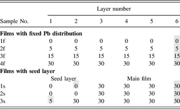
Film-forming solutions were prepared by mixing appropriate amounts of zirconium monosolvate isopropylate Zr[O(CH3)2CH]4(CH3)2CHOH, titanium tetraisopropoxide Ti[O(CH3)2CH]4, and anhydrous lead acetate Pb(CH3COO)2 in 2-methoxyethanol at room temperature. Reference Kotova, Vorotilov, Seregin and Sigov49 The final solution concentrations in terms of the sum of the Ti and Zr alkoxides was 0.25 M. Lead acetate was synthesized by reacting PbO with acetic acid in acetic anhydride that allows one to obtain an anhydrous material free of oxyacetates and possessing sufficient reactivity. Reference Kotova, Vorotilov, Seregin and Sigov49 The PbZr0.48Ti0.52O3 films were formed on silicon wafers with a Pt (150 nm)/TiO2 (10 nm)/SiO2 (300 nm)/Si structure (produced by Inostek, Seoul, South Korea). The PZT film-forming solution was applied in six layers by spin-on deposition (spin speed 2700 rpm) with an intermediate IR drying at 180 °C for 5 min and pyrolysis at 400 °C during 10 min for each layer. After the last layer was formed, the films were crystallized by annealing in a furnace at 600 °C for 15 min. Four samples (Nos. 1f–4f) were prepared from solutions with fixed Pb excess: 0, 5, 15, and 30 wt% (see Table I). Three samples were prepared with a low-Pb-content sublayer (Nos. 1s–3s, see Table I). Sample Nos. 1s and 2s were formed by deposition of two layers of a solution without lead excess (1s and 2s), and another sample, by deposition of a single layer of the solution with 5 wt% Pb excess (3s). Samples 1s and 3s were subjected to crystallization at 600 °C before the deposition of the main layers. The main film was deposited onto crystallized and noncrystallized seed layers by four or five applications of a PZT solution with a 30 wt% Pb excess. The top Pt electrodes with thickness of 20 nm and area of ∼10−3 cm2 were formed by DC magnetron sputtering with a shadow Si mask having a thickness of ∼350 μm.
PZT films with the fixed Pb excess and seed layers: Pb excess in the film-forming solution (wt%) in each layer. All films consist from 6 spin coated layers.

The layer subjected to crystallization at 600 °C is marked in gray.
The thickness and refractive index of the PZT films were found by spectral ellipsometry (SE-850, Sentech Instruments GmbH, Berlin, Germany) to be within the ranges 215–300 nm and 2.53–2.75, respectively. The film structure was studied using a DRON-3 diffractometer (DRON-3 diffractometer, NPP Burevestnik, St. Petersburg, Russia; Θ–2Θ scan mode, Cu Kα radiation). The hysteresis loops were measured by the standard Sawyer–Tower method with a sinusoidal voltage sweep within the range ±6 V and signal frequency of 64 Hz. SEM measurements were performed with JSM-7001F microscope (JEOL Ltd., Tokyo, Japan).
III. EXPERIMENTAL RESULTS AND DISCUSSION
A. Effect of the seed layer on the polarization
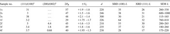
Figures 1(a) and 1(b) presents X-ray diffraction (XRD) patterns measured in the PZT films deposited with and without seed layers, respectively. It is seen that all the films show a predominant (111) texture along the volume diagonal and a weaker texture along either (100) “a” axis or (001) “c” axis. The ratios of the reflection intensities found from the diffraction peaks are listed in Table II. In film Nos. 1s and 3s, in which seed layers were subjected to crystallization, the reflection intensity ratios are 31 and 38, respectively, with the second kind of texture practically suppressed. Thus, the crystallization of low-Pb-excess seed layers significantly enhances the Pe (111) texture. The grain sizes found from the half-width of diffraction peaks are listed in Table II.
X-ray diffraction patterns of sample (a) Nos. 1s–3s and (b) Nos. 1f–4f.

Film texture, remanent polarization, coercive voltage, thickness, and average grain size, found from XRD and SEM measurements (P R [µC/cm2], V C [V], d [nm], L [nm]).

a Reflection intensity ratio.
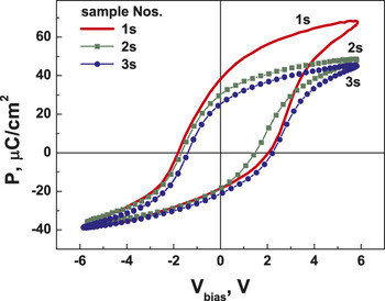
Figure 2 shows the hysteresis loops measured for the films with seed layers. It is seen that the crystallized seed layer without a Pb excess provides the highest P magnitudes as compared with crystallized seed layer deposited from the 5 wt% Pb excess solution and noncrystallized layer deposited from the solution without a Pb excess. Table II presents the parameters for hysteresis loops measured for the films with a fixed Pb excess. The highest P values are observed in film No. 3f at a fixed Pb excess of 15 wt%, but these values are smaller than those for the crystallized seed layer without Pb excess.
Polarization versus bias voltage measured in sample Nos. 1s–3s.

Note that, for most of the samples, the positive coercive voltage is higher than that of negative sign, which indicates that there is a negative internal electric field in the films. In addition, the magnitude of +P R exceeds that of −P R. We have observed a similar behavior earlier in CSD PZT films with a Pb excess of 15 wt%. Reference Delimova, Guschina, Yuferev, Grekhov, Seregin, Vorotilov and Sigov50,Reference Delimova, Guschina, Yuferev, Ratnikov, Zaiceva, Sharenkova, Seregin, Vorotilov and Sigov51 We assume that the asymmetry in ±P R may be caused by a self-polarization, which cannot be switched by the electric field. We attribute the self-polarization to the flexoelectric effect in which the in-plane lattice mismatch between the bottom Pt layer and a PZT film induces a strain gradient across the film thickness, and this gives rise to the flexoelectric polarization. Reference Delimova, Guschina, Yuferev, Ratnikov, Zaiceva, Sharenkova, Seregin, Vorotilov and Sigov51 The strain (compression) is negative, but the strain gradient is positive in the coordinate system of our experiment, and, therefore, the unswitchable self-polarization is positive. The incomplete compensation of the flexoelectric polarization charge can produce a negative internal electric field, which is manifested in the asymmetry of the hysteresis loops.
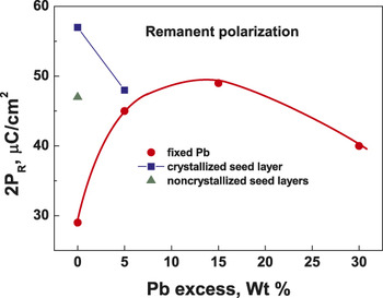
The effect of low-Pb-excess seed layers on the polarization is clearly seen in Fig. 3, in which the remanent polarizations plotted as a function of the Pb excess are compared for all the films under study. It is seen that using low-Pb-excess seed layers in sample Nos. 1s–3s provides a substantially higher polarization magnitude as compared with those in the films with the fixed 0–5% Pb excess across the film thickness. A possible reason is the enhancement of the Pe (111) texture in the films with the crystallized seed layer Nos. 1s and 3s, and, probably, the large grain size in film No. 2s.
Remanent polarization as a function of the excess Pb content in the film-forming solution.

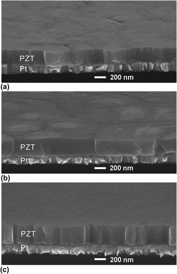
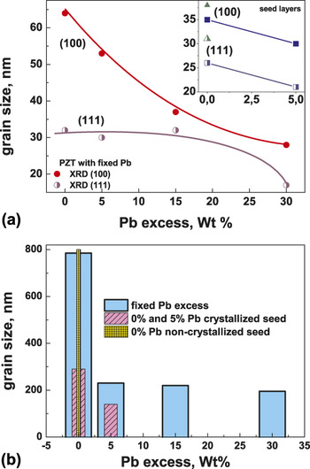
The average grain sizes found from the plan-view and cross-sectional SEM images of the film are listed in Table II. To illustrate the wide scatter of grain sizes in the films, Fig. 4 shows the cross-sectional SEM images of sample Nos. 1s–3s in which the largest (2s) and smallest (3s) grain sizes can be seen. Noteworthy is the difference in the grain size found from XRD and SEM measurements. The point is that, in the first case, the grain size is the size of a coherent-scattering region and, in the second, it is the physical size of crystallites, determined from SEM images. Figure 5(a) shows dependences of the grain size found from the half-width of (100) and (111) XRD peaks on the Pb excess content for sample Nos. 1f–4f. The inset in the upper right-hand corner of the figure shows the same kind of dependences for sample Nos. 1s–3s with seed layers. The grain sizes decrease with increasing Pb content, which agrees with the data previously furnished by TEM. Reference Sigov, Vorotilov and Zhigalina30 Similar behavior is exhibited by grain sizes obtained from SEM measurements in films with and without a seed layer, see Fig. 5(b). Comparison of the results for crystallized seed layers deposited from solutions without a Pb excess and with a 5 wt% Pb excess shows that the crystallization of a seed layer makes smaller the grain size because the first crystallization step occurs in very thin layer and the grain growth is restricted by the film thickness despite the low nucleation rate. It seems that these small, but highly oriented grains serve as nucleation centers for growth of highly (111) textured films. Among the films prepared on a crystallized seed layer, the film without a Pb excess demonstrates larger grain sizes due to lower nucleation rate (sample No. 1s).
Cross-sectional SEM images of samples (a) No. 1s (b) No. 2s and (c) No. 3s.

Grain sizes as a function of the excess Pb content in the film-forming solution found from (a) the half-widths of (100) and (111) X-ray diffraction peaks and (b) the SEM measurements.

In the case when the seed layer is not subjected to crystallization before the main film (sample No. 2s) is deposited, we observed very large grain sizes with wide scatter because the crystallization proceeds in the whole film body at a low nucleation rate at the interface due to the low Pb content. However, we observe in this case the loss of a strong (111) texture, the (111)/(100) ratio being nearly the same as that for films with a fixed 15–30 wt% Pb excess. We suggest that the reason is the Pb diffusion during the heat treatment: the Pb concentration at the Pt/PZT interface may be low only in the first stage of the crystallization process and become uniform as a result of the Pb diffusion from the upper part of the film with high Pb concentration. Summarizing the results obtained, we can state that the combination of low-Pb-excess seed layers and a 30 wt% Pb excess in the main film dramatically affects the PZT film structure: size of Pe grains and their orientation, which can be used for improving the electrical performance of PZT films.
B. Effect of the seed layer on the grain-boundary conduction
A specific feature that manifests itself in the current–voltage curves of PZT as a dip was described as the so-called NDR by Scott et al. Reference Scott, Melnik, Cuchiaro, Zuleeg, Araujo, McMillan and Scott52 and attributed to the double injection of both electrons and holes into the PZT from the electrode. Later, the NDR, i.e., a negative slope, plateau, or inflection was observed Reference Daniel Chen, Udayakumar, Li, Gaskey and Eric cross53–Reference Podgorny, Vorotilov and Sigov58 in current–voltage dependences of PZT and BST and attributed to the trap filling process, Reference Daniel Chen, Udayakumar, Li, Gaskey and Eric cross53–Reference Alkoy and Shiosaki55 diffusion in terms of the Dawber and Scott model, Reference Scott, Morrison, Miyake, Zubko, Lou, Kugler, Rios, Zhang, Tatsuta, Tsuji and Leedham56 and polarization recovery. Reference Podgorny, Sigov, Vishnevskiy and Vorotilov57,Reference Podgorny, Vorotilov and Sigov58 Earlier, Delimova et al. found Reference Delimova, Gushchina, Yuferev and Grekhov48 a correlation between the grain-boundary conduction and the current peaks that appear in the current polarization dependences and look like the NDR. This correlation was confirmed by the local current distribution measured in the films by the scanning spreading resistance microscopy (SSRM). It was shown that the emergence of NDR in the PZT films depends on (i) whether the current flows inside the ferroelectric phase (epitaxial films) or outside, along grain boundaries, and (ii) whether the applied bias is directed in the polarization direction or against it.
We measured the current–voltage characteristics of the Pt/PZT/Pt samples under study at different preliminary polarizations. The bias was applied as a sequence of 0.1 V steps with duration of 0.2 s, and the current was recorded at the end of a step. The voltage was varied from 0 to 3 V and then back to zero. For both the bias directions, the measurements were made at different preliminary polarizations. The switching times of the ferroelectric domains in the PZT are ∼1–10 ns. Reference Waser and Klee59 For the parameters we used for the external circuit and samples under study, the decay time of the experimentally measured currents I was ∼10 ms, so it takes about 0.2 s for I to decrease to the technical zero of ∼pA. For times longer than 0.2 s, the current measured in the experiment cannot be caused by the domain switching and should be attributed to the trap recharging and other relaxation processes. To correctly study the current polarization dependences, we need a reliable reference point, and this can be the depolarization state. For this purpose, the film was depolarized before each measurement by the Sawyer–Tower method in which the external decaying sinusoidal voltage is applied to the PZT capacitor, thereby producing a depolarization state. Then a film is polarized in a certain direction by application of a ±6 V bias pulse with width of 2 s. Note that this depolarization procedure allows each measurement of the current to start under the same initial conditions, which also include the same charge state at the interfaces of the film.
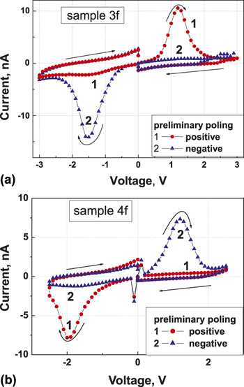
All the samples demonstrate a clockwise current hysteresis with a current peak on its up-going branch and no peak on the down-going branch. In addition, the current magnitude depends on the voltage rise rate, which is typical of a capacitive current. At the same time, our results revealed two groups of samples for which the appearance conditions of current peaks differ fundamentally. Namely, the current in sample Nos. 1f–3f, 2s–3s is higher at both bias directions if the bias and polarization directions coincide, compared with the case when they are opposite [Fig. 6(a)], which is not expected. Previously, we have found a similar current polarization dependence in an epitaxial PZT film in which the current flows within the ferroelectric phase. Reference Delimova, Gushchina, Yuferev and Grekhov48 Thus, our polarization dependence of the current indicates that the grain boundaries in film Nos. 1f–3f, 2s–3s are in all probability nonconductive. In sample Nos. 4f and 1s [Fig. 6(b)], by contrast, a higher current is observed when the bias is directed against the polarization. A similar behavior has been observed earlier in MOCVD PZT films Reference Delimova, Gushchina, Yuferev and Grekhov48 in which the PbO phase is formed at grain boundaries during the annealing, with the conduction of the grain boundaries themselves thereby provided. Reference Lee, Ku, Cho, Lee, Shin and Park60 Therefore, we can assume that film Nos. 4f and 1s have conductive grain boundaries.
Current–voltage dependences of samples (a) No. 3f and (b) No. 4f, measured at two preliminary poling ±P R.

To study the possible grain-boundary conductivity of the films, local current distributions were measured by SSRM. This contact-mode AFM method yields the film surface topography and the local-current map simultaneously. All AFM measurements were made with an Ntegra Aura (NT-MDT Spectrum Instruments, Moscow, Russia) scanning probe laboratory. The images were obtained using rigid (k = 5−20 N/m) conductive probes with a wear-resistant diamond-coated cantilever, which retained their conductive properties even when voltages of ±10 V were applied. An external bias of ∼5–10 V was applied to the bottom electrode, while the top electrode was grounded.
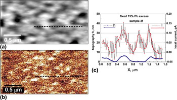
Figure 7 shows 2D-images of (a) AFM topography and (b) local current map of film No. 3f, simultaneously produced by SSRM. Here, the white areas of increased conductivity in (b) are correlated with the light areas in (a), which corresponds to heights of grains. Figure 7(c) shows topographic and local-current signal profiles found from the data of Figs. 7(a) and 7(b). The minima in the topographic signal correspond to grain boundaries. It can be seen that the current flows across the grains since the zero-current positions coincide with the grain boundaries, thereby indicating that the grain boundaries are nonconductive. Film Nos. 1f–2f, 2s–3s show similar topographic and zero-current profiles, which confirms that the grain boundaries are nonconductive.
2D images of (a) AFM topography and (b) local current map of PZT film No. 3f, produced by SSRM. The dotted line corresponds to the position of the profile. (c) Signal profiles of the topography (left scale, circles) and local current (right scale, triangles) in film No. 3f along the profile shown at a length of 1.5 µm; the zero signal level on the current scale does not coincide with the zero level for the topography. The line for the current signal is drawn as a guide to the eye.

Figure 8 presents the 2D-images of (a) AFM topography and (b) local current map for film No. 4f, produced by SSRM. Here, the white areas of increased conductivity are correlated with the topography of the intergrain space. This is more clearly shown by Fig. 8(c), which shows the topographic and local-current signal profiles found from the data of (a) and (b). It can be seen that the positions of the current maxima coincide with those of the grain boundaries, which indicates that the grain boundaries are substantially more conductive than the grains themselves. Finally, the AFM images of the topography and local current map, obtained for film No. 1s, shows that the positions of the current maxima are correlated with those of both the grains and grain boundaries, which indicates, that the current flows both across the grains and along the grain boundaries.
2D images of (a) AFM topography and (b) local current map of PZT film No. 4f, obtained by SSRM. The dotted line corresponds to the position of the profile; (c) Signal profiles of the topography and local current in film No. 4f across the profile shown in (a) and (b); the zero signal level on the current scale does not coincide with the zero level for the topography. The line for the current signal is drawn as a guide to the eye. The black arrows indicate the positions of grain boundaries.

The experimental results furnished by both the methods demonstrate a correlation between the current peak measured in the I–V curves and the experimentally determined conductivity of grain boundaries. Indeed, in sample Nos. 1f–3f, 2s, 3s, for which the current peak is observed when the bias and polarization directions coincide, the grain boundaries are nonconductive. By contrast, in sample Nos. 4f and 1s, for which the current peaks are observed when the bias is directed against the polarization, the grain boundaries are conductive.
The effect of the excess Pb content and seed layer on the grain-boundary conduction was found in the study. By itself, the segregation of lead at grain boundaries during the PZT annealing is widely recognized and has been repeatedly observed in films prepared by MOCVD Reference Lee, Ku, Cho, Lee, Shin and Park60,Reference Park and Chung61 and magnetron sputtering. Reference Afanasiev, Mosina, Petrov, Pronin, Sorokin and Tarakanov62–Reference Pronin, Senkevich, Kaptelov and Pronin64 Observations of local currents flowing along grain boundaries in MOCVD PZT films have also been reported. Reference Fujisawa, Shimizu, Horiuchi, Shiosaki and Matsushige65,Reference Gushchina, Ankudinov, Delimova, Yuferev and Grekhov66 As for the CSD PZT films, the segregation of the PbO phase at grain boundaries and Pt/PZT interface was found only at a 50 wt% excess of Pb. Reference Sigov, Vorotilov and Zhigalina30 Therefore, the observation of conductive grain boundaries in a film with a 30 wt% Pb excess is the new result. As shown earlier by TEM studies, the high Pb content stimulates the nucleation of (100) perovskite grains due to the good lattice matching. Because of the high growth rate, especially in the (111) and (100) directions, perovskite grains become smaller and not all of these can grow across the whole thickness of a film. Reference Vorotilov, Yanovskaya, Turevskaya and Sigov67 So, we can suggest that a large grain boundary area with possible lead oxide conductive inclusions exists in this case. It is noteworthy that, among the first three films with seed layers, the grain-boundary conduction is only observed in film No. 1s for which the first crystallization step occurs in the seed layer without a Pb excess. In this case, the grain-boundary conduction may be due to the large number of defects associated with the lead deficiency and oxygen vacancies. During the cooling after the seed layer is crystallized, the vacancies can trap electrons and thereby provide a hopping conduction along the grain boundaries.
As for the emergence of NDR, we assume that the current peaks are due to the trap recharging caused by the applied bias and polarization. Reference Delimova, Gushchina, Yuferev and Grekhov48 In the case of conductive grain boundaries, the traps are involved in the screening of the polarization charge at grain boundaries. A current peak arises when the bias is opposite to the polarization direction, which seems to be natural. It is quite another matter in the case of nonconductive grain boundaries, in which the current peak arises when the bias and the polarization direction coincide and the traps are situated within grains. We assume that the trap recharging is controlled by the joint effect of the polarization on the internal electric fields and on the probability of carrier emission from impurity centers. Since the transient current grows as the voltage rise rate becomes higher, this effect can be important and should be taken into account in FeRAM devices whose readout operation assumes recording the magnitude of the polarization switching current.
IV. CONCLUSIONS
The two-step crystallization process of CSD PZT films based on a low-Pb-content seed layer was studied. The first crystallization step (seed layer) is performed at a low Pb excess (0–5 wt%) to form strongly (111) oriented Pe grains. The next crystallization step is performed with a 30 wt% excess of Pb to prevent formation of Py inclusions and accelerate the growth of Pe grains. It is shown that the combination of a low-Pb-excess seed layer and a 30 wt% Pb excess in the main film dramatically affects the PZT film structure: size of Pe grains and their orientation, which can be used for improving the electrical performance of PZT films.
PZT film demonstrates a high (111) texture with complete suppression of the (100) orientation in the case when the seed layer is subjected to crystallization before the main film is formed. In this case, the grain size is larger and the polarization is stronger when a solution having no Pb excess is used. By contrast, the grain size sufficiently increases due to the low nucleation rate at the Pt/PZT interface if the low-Pb-content seed layer is not crystallized before other layers are deposited, but the film texture is not changed in this case.
It was demonstrated by the transient-current analysis and SSRM local current distributions that the lead content and the crystallization of the seed layer affect the grain-boundary conduction, which, in turn, influences the polarization dependence of the transient currents. This effect may be important and should be taken into account in FeRAM devices whose readout operation is based on recording the polarization switching current.
ACKNOWLEDGMENTS
This study was supported by the Ministry of Education and Science of the Russian Federation, project No. 11.2259.2017 (K.V., D.S., and A.S.), and by program No. 1 of the Russian Academy of Sciences.