I. INTRODUCTION
Tin dioxide, SnO2, is widely used as gas sensor materialReference Batzill and Diebold1 and highly Sb- or F-doped as transparent contact.Reference Jarzebski and Morton2 For these traditional applications, SnO2 is prepared with a low material quality—typically polycrystalline. To render SnO2 a transparent semiconductor in its own right and to study its intrinsic material properties, a significantly higher material quality is mandatory: electrons at moderate—semiconductor like—donor concentrations are sensitive to scattering and/or compensation by grain boundaries, crystal defects, and impurities, which is far less the case in transparent oxide-based contacts with high intentional donor concentration that clearly exceeds the concentration of other impurities and defects.
This paper reviews results on n-type doping, the difficulty to achieve p-type conductivity, the role of the interface region, and that of the surface electron accumulation layer (SEAL) for electron transport in high-quality SnO2 films. Taking into account, the interface carrier system in the films was vital for the interpretation of the transport measurement results. The methodology used here can also be applied to the transport analysis in other thin-film materials such as other transparent semiconducting oxides. Our semiconductor-like approach aimed at the basic understanding (rather than targeting an application) distinguishes this work from the tremendous body of work on SnO2 nanoparticles, transparent contacts, and gas sensors. Many published results on n-type (and even p-type) doping of SnO2 films were achieved with cost-effective low-quality material (e.g., prepared by spray pyrolysis) and doping concentrations well into the alloying regime (even exceeding 20%), making it hard to understand whether the measured conduction is a bulk effect, due to grain boundaries or due to secondary phases.
II. METHODS
In an effort to study SnO2 material properties that are not dominated by defects, grain boundaries, and unintentional impurities, plasma-assisted molecular beam epitaxy (PA-MBE) was used to prepare high-quality single-crystalline SnO2 thin films. Due to a lack of native or lattice-matched substrates, the SnO2(101) films were grown on r-plane sapphire [Al2O3(10–12)].Reference White, Tsai, Wu and Speck3 The lattice mismatch between SnO2 and the substrate resulted in a highly dislocated interface region with a rapidly decreasing dislocation density at increasing thickness as seen in cross-sectional transmission electron microscopy images.Reference White, Tsai, Wu and Speck3, Reference Vasheghani Farahani, Veal, Sanchez, Bierwagen, White, Gorfman, Thomas, Speck and McConville4 To limit the relative contribution of this few 100-nm-thick defective region, the films were grown to a total thickness of ∼1 μm. X-ray diffraction (XRD) was used to further gauge the structural quality: While omega-2-theta scans indicated phase pure SnO2(101) with a single in-plane and out-of-plane orientation, the omega rocking curve full width at half maximum (FWHM) of typically 0.2–0.4° indicated a lower mosaicity (i.e., higher quality) than other published results.Reference White, Tsai, Wu and Speck3 The surface of the films is facetted, which has negligible influence on the overall transport properties in the film (e.g., by surface roughness scattering) due to the large film thickness.
The use of highly pure (7N) source materials and the ultrahigh vacuum environment of the PA-MBE chamber, both, ensured a high purity of the grown films.Reference White, Tsai, Wu and Speck3 Calibrated secondary ion mass spectroscopy (SIMS) measurements show hydrogen concentrations around 4 × 1017 cm−3 and carbon, nitrogen, indium, gallium, and aluminum concentrations below 1 × 1017 cm−3.Reference White, Tsai, Wu and Speck3 While it is virtually impracticable to cover all possible impurities by SIMS measurements, the carrier concentration and mobility can reveal impurities that act as donors (increase electron concentration) or as compensating acceptors (decrease electron concentration and mobility).
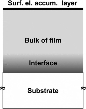
The transport properties of undoped, Sb-doped, In-doped, and Ga-doped films were studied by Hall and conductivity measurements in van der Pauw geometry at room temperature.Reference White, Bierwagen, Tsai and Speck5 These measurements integrate the transport properties across the entire depth of the sample, which makes it necessary to understand what carrier systems are present in the sample. Figure 1 schematically summarizes potential carrier systems in thin-film samples:
Schematics of parallel carrier systems present in a thin-film sample. All these systems can be present and contribute to conductivity and Hall measurements.

(i) The bulk of the film, intuitively, is the source of the film conductance. This conductance and sheet carrier concentration should scale linearly with film thickness, and a large film thickness is beneficial for studying unintentional or intentional doping as it maximizes the relative contribution of this doping to the sample transport properties.
(ii) Transparent semiconducting oxides are prone to the formation of SEALs. These SEALs consist of a high volume concentration of electrons at the surface that penetrate only a few nanometers into the sample and should contribute to the conduction in a sample. It seems straightforward to use thin films to increase the relative contribution of the SEAL to the overall transport.
(iii) However, the interface or interface region between the substrate and the bulk of the film can host another (even highly conductive) carrier system—either a true sheet carrier system due to band bending at the interface or a volume carrier system related to impurities or dislocations in the interface region. For example, interface carrier systems have been identified for homoepitaxial InP,Reference Rakennus, Tappura, Hakkarainen, Asonen, Laiho, Rolfe and Dubowski6 for InN,Reference Bierwagen, Choi and Speck7 and for SnO2.Reference White, Bierwagen, Tsai and Speck5 Consequently, the existence of interface carriers has to be considered in the interpretation of transport data, and a potential interface contribution has to be ruled out when assigning thin-film transport properties to the SEAL. One way to deal with the interface system is to grow the system of interest on top of the interface region and systematically removing the interface region transport contribution from the total transport result in the data analysis, which has been done in the Sb-doping study of SnO2.Reference White, Bierwagen, Tsai and Speck5 Alternatively, the interface region can be made semi-insulating by suitable doping with deep acceptors,Reference White, Bierwagen, Tsai and Speck8 which has also been used for the Ga- and In-doping study presented here.
(iv) Finally, insulating substrates are necessary to study the thin-film transport properties. Oxide substrates are usually insulating but some oxides (e.g., TiO2 or SrTiO3) could turn conductive during film growth in a high vacuum and high temperature environment. For this reason, TiO2(110), which is suitable for SnO2 growth due to the common crystal structure, could not be used for transport studies.Reference Tsai, White and Speck9 In contrast, sapphire, Al2O3, remained insulating after growth and was used as substrate for all transport studies.
The identification of the carrier type is a crucial issue when it comes to finding p-type conductivity in SnO2 and related oxides. For example, artifacts in Hall measurements can lead to an erroneous assignment of p-type conductivity to actually n-type material.Reference Ohgaki, Ohashi, Sugimura, Ryoken, Sakaguchi, Adachi and Haneda10, Reference Bierwagen, Ive, Van de Walle and Speck11 The application of alternative techniques such as hot probe measurements (using the Seebeck effect) or capacitance–voltage (CV) measurements was suggested to verify the carrier type,Reference Look12 and care has to be taken with CV measurements as they may indicate the wrong carrier type either due to artifacts.Reference Bierwagen, Nagata, Ive, Van de Walle and Speck13
III. RESULTS AND DISCUSSION
A. Doping control of the SnO2 conductivity
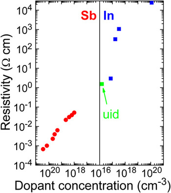
Figure 2 gives an overview of the SnO2 bulk resistivity (inverse of conductivity) as a function of intentional doping. SnO2 and many other transparent semiconducting oxides are n-type conducting even though they have not been intentionally doped with donors. The reason for this unintentionally doped (uid) n-type behavior is still being debated with donor candidates comprising intrinsic point defects, incorporated hydrogen, or other impurities.Reference Singh, Janotti, Scheffler and Van de Walle14 The resistivity of the uid SnO2 films that were the basis of our doping studies was in the range of 0.1–1 Ω cm at volume electron concentrations around 1017 cm−3 and mobilities up to 100 cm2/Vs.Reference White, Tsai, Wu and Speck3 Numerous studies showed uid SnO2 films with electron concentrations exceeding 1019 cm−3 at mobilities below 30 cm2/Vs,Reference White, Bierwagen, Tsai and Speck5 which indicated a much lower quality due to impurities and/or thin highly dislocated films. On the other hand, highly pure true bulk samples have been demonstrated with a resistivity of 3 Ω cm at a volume electron concentration of 8 × 1015 cm−3 and a mobility as high as 260 cm2/Vs,Reference Fonstad and Rediker15 clearly exceeding the material quality of our thin films. This bulk-like material quality cannot be reached with our films due to the detrimental effects of lattice mismatch—a correlation that has already been observed with ZnO.Reference Tsukazaki, Ohtomo and Kawasaki16
Resistivity of SnO2 as a function of doping concentrations: donor doping with Sb. Compensating acceptor doping with In. An “uid” sample is given as reference. The conductivity was always n-type—irrespective of the dopant.

Substitutional antimony on a Sn site of the SnO2 lattice acts as a donor and has been used for the application of SnO2 as a transparent conducting oxide (TCO).Reference Jarzebski and Morton2 A systematic doping study with Sb concentrations ranging from semiconductor-like 1018 cm−3 up to the TCO regime showed a doping efficiency of 100%, i.e., each Sb atom acted as a donor.Reference White, Bierwagen, Tsai and Speck5 With increasing Sb concentration, the resistivity decreased controllably down to the TCO regime with 6.7 × 10⁻⁴ Ω cm, an electron concentrations of 2.6 × 1020 cm−3, and a mobility of 36 cm2/Vs.Reference White, Bierwagen, Tsai and Speck5 Even this high Sb concentration did not show any detrimental effects on the structural film properties: the film remained phase pure with the same low mosaicity (omega rocking curve FWHM of 0.31°) as an undoped reference film grown under the same conditions.Reference White, Bierwagen, Tsai and Speck5 An overview of the transport properties of various TCOs has been compiled in Ref. Reference Toyosaki, Kawasaki and Tokura17. This reference also reports that a Ta concentration of 5% in epitaxial SnO2 on TiO2(110) resulted in a record low resistivity of 1.1 × 10⁻⁴ Ω cm (comparable to the best In2O3:Sn, “ITO”). However, the potential role of the TiO2 substrate conductivity to this result is unclear.
Doping with In (or Ga), in contrast, increased the SnO2 resistivity up to approximately 104 Ω cm. This semi-insulating behavior rather than p-type conductivity is discussed next in more detail.
B. Doping with deep acceptors: In and Ga
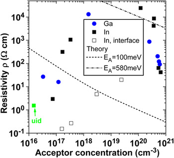
Group IIIA elements are natural acceptor candidates if they occupy a Sn site in the SnO2 lattice. Of the group IIIA elements, indium and gallium have been theoretically predicted shallow acceptors with an activation energy about 100 meV.Reference Singh, Janotti, Scheffler and Van de Walle14 With the inclusion of polaronic hole localization, however, In and Ga have been predicted to be deep acceptors with activation of 580 and 760 meV, respectively.Reference Lany and Zunger18
Initial In-doping experiments of SnO2 only showed a gradually increasing average resistivity with increasing In concentration, as shown by the open symbols in Fig. 3. This behavior is an artifact of the dominating contribution of the highly n-type conductive uid interface region.Reference White, Bierwagen, Tsai and Speck8 Turning the interface region semi-insulating by high In-doping (on the order of 1020 cm−3)Reference White, Bierwagen, Tsai and Speck8 enabled the investigation of the true bulk resistivity of In- and Ga-doped SnO2Reference Tsai19: the closed symbols in Fig. 3 show a steep increase of the resistivity as the In or Ga concentration compensates the uid bulk donor concentration of few 1017 cm−3. Above an acceptor concentration of 1018 cm−3, the uid donors are fully compensated and the bulk is semi-insulating with a resistivity on the order of 104 Ω cm. Beyond the full compensation, p-type conductivity and a decreasing resistivity with increasing acceptor concentration would be expected for shallow acceptors. This theoretical trend is indicated by the broken lines in Fig. 3, which show calculated resistivities based on a hypothetical hole mobility of 1 cm2/Vs and a hole concentration calculated with a charge balance equation (using a hole effective mass of 1.35 times the free electron massReference Schleife, Varley, Fuchs, Rödl, Bechstedt, Rinke, Janotti and Van de Walle20 and the theoretically predicted hole activation energies of 100 or 580 meV).Reference White21 Comparison with the measured resistivity clearly favors the predicted deep acceptor over the shallow acceptor hypothesis as the resistivity of the In- or Ga-doped SnO2 remains high even when the In or Ga concentration was increased by two orders of magnitude up to 1020 cm−3. The steeply decreasing (n-type) resistivity at In or Ga concentrations above 3 × 1020 cm−3 coincided with the formation of In2O3 or Ga2O3 secondary phases (measured by XRDReference White, Bierwagen, Tsai and Speck8, Reference Tsai19) in the SnO2 film, which are themselves uid n-type conductive.
Resistivity of SnO2 as a function of In and Ga concentrations. The broken lines indicate hypothetical values for different acceptor ionization energies. To demonstrate the misleading effect of the highly n-type conductive uid interface region, the open symbols represent samples where the interface region was not made insulating.

C. Surface conductivity
The SEAL on SnO2 largely influences contact properties by preventing the formation of Schottky contacts and promoting the formation of ohmic contactsReference Bierwagen, White, Tsai, Nagata and Speck22, Reference Nagata, Bierwagen, White, Tsai and Speck23 and is likely at the root of the chemical sensor functionality of SnO2. InN is an example where the SEAL sheet resistance is low (on the order of 103 Ω/square) and has significant impact on the overall sample conduction.Reference Bierwagen, Choi and Speck7, Reference Swartz, Tompkins, Giles, Myers, Lu, Schaff and Eastman24 In SnO2, the situation seems to be different:
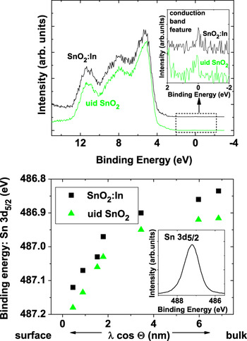
Lightly (low 1018 cm−3) indium-doped SnO2 films were used to make the bulk of the films insulating. Figure 4 shows x-ray photoelectron spectroscopy measurements, which only probe the near-surface region, of the lightly In-doped and a uid SnO2 film. The presence of conduction band electrons together with a clear downward bending of the bands toward the surface indicates the presence of a SEAL in both films.Reference Nagata, Bierwagen, White, Tsai, Yamashita, Yoshikawa, Ohashi, Kobayashi, Chikyow and Speck25 In- or Ga-doped SnO2 films used for the previous section with the same light bulk In or Ga doping (low 1018 cm−3) but with additional high In-doping in the interface region to render this region insulating should have a residual conductivity due to the SEAL only. The sheet resistance of these samples was on the order of 108 Ω/square, which can be considered a lower bound estimate of the SEAL sheet resistance, and indicates that the SnO2 SEAL is highly resistive.
XPS measurements of a “uid SnO2” and a lightly (3 × 1018 cm−3) In-doped SnO2 film (“SnO2:In”). Positive binding energies correspond to electrons below the Fermi level. Zero binding energy corresponds to the Fermi level. (Top): Valence band spectra. Inset: Magnified conduction band features due to SEALs. (Bottom): Band bending as extracted from the binding energy of the Sn 3d 5/2 core level peak (inset) at different probing depth [“λ cos(Θ)”]. Since the core level has a fixed energy separation from the band edges, the band bending follows the energy versus depth behavior of the core levels.

IV. SUMMARY
In summary, the transport properties of undoped, donor- (Sb), and acceptor (In, Ga)-doped SnO2 thin films were reviewed. To ensure high material quality, these films were grown by PA-MBE. For the interpretation of the transport measurements, it was important to consider all potential carrier systems in the samples (the substrate, the substrate–film interface region, the bulk of the film, and the film surface). While the frequently used TiO2 substrates turned conductive after MBE growth, the substrates used for this study, r-plane Al2O3, remained insulating. A highly conductive n-type interface region was found that could be wrongly attributed to surface conductivity and could lead to severe misinterpretation of the acceptor doping results. In this study, the interface region was made insulating by overcompensation with deep acceptors. The doping experiments showed that Sb behaves as a shallow donor with 100% doping efficiency up to the maximum concentration of 2.6 × 1020 cm−3 studied here. At this highest doping level, the resistivity of 6.7 × 10⁻⁴ Ω cm was in the TCO regime. In and Ga, in contrast, behaved as deep acceptors, likely due to polaronic hole localization, which turned the SnO2 semi-insulating at resistivities above 104 Ω cm. At In or Ga concentrations >3 × 1020 cm−3, the films turned more n-type conductive again likely due to the formation of secondary uid n-type In2O3 and Ga2O3 phases. Despite its big impact on contact properties, the SEAL was extremely resistive at a sheet resistance above 108 Ω, which is negligible in comparison to the sheet resistance of uid- or donor-doped SnO2 thin films of any thickness. The methodology used in this study can also be applied to other materials, such as other semiconducting oxides.