I. INTRODUCTION
Transition metal carbides and nitrides are successfully employed as wear- and oxidation-resistant thin films. The research trend is toward multinary compounds to achieve film materials with enhanced and optimized properties for various applications. In this study, we report on the Ti–Si–C–N system, inspired by and extending the limits of the two successfully applied ternaries Ti–Si–NReference Flink, Beckers, Sjölen, Larsson, Braun, Karlsson and Hultman1 and Ti–C–N.Reference Karlsson, Hultman, Johansson, Sundgren and Ljungcrantz2 The quarternary system is challenging in terms of the several binary and ternary phases that it comprises, as well as unresolved issues about element substitution and segregation in the different phases. While the Ti–C–N system exhibits complete solid solubility in the B1 cubic phase, the Ti–Si–N system is characterized by strong segregation of Si to form TiN and polymorphic Ti–Si and Si3N4 phases. Mixing all four elements may also give rise to competing SiC and CNx formation. These effects are highly dependent on composition, as shown in this work.
The Ti–Si–C–N system has been explored to some extent in thin films made by chemical vapor deposition (CVD),Reference Abraham, Choi, Kang and Kim3–Reference Kuo and Liao6 plasma enhanced CVD (PECVD),Reference Guo, Ma and Xu7–Reference Ma, Ma and Xu10 and magnetron sputtering from various Ti–Si–C compound targetsReference Shtansky, Levashov, Sheveiko and Moore11, Reference Shtansky, Levashov, Sheveiko and Moore12 or Ti targets used in trimethylsilane (CH3)3SiH and N2.Reference Xu, Nie and Wei13, Reference Wei, Langa, Rincon and Arps14 Magnetron sputtering of Si has also been combined with arc deposition of Ti in an atmosphere with CH4 and N2.Reference Jeon, Choi, Chung and Kim15 Cathodic arc is known to produce dense and defect-rich films in processes that can be readily applied at an industrial scale. However, it is only recently that arc-deposited films in the Ti–Si–C–N system have been reported, resulting from deposition processes with conventional Ti–Si compound cathodes used in a mixture of N2 and CH4 in an industrial scale system [Reference Johnson, Rogström, Johansson, Odén and Hultman16] as well as in combination with N2 and C2H2 in a smaller system.Reference Chang and Hsieh17
In this study, we advance beyond standard cathode materials and report on reactive arc evaporation from ternary Ti3SiC2 cathodes in N2 gas. The use of compound cathodes is of interest for rational utilization of coating equipment and simple process control, compared to setups with a multitude of elemental cathodes. Our method offers relatively high concentrations of Si and C, while maintaining the high film density and crystallinity characteristic of arc deposition. We thus present a path to explore carbonitride films with a unique range of compositions and structures.
II. EXPERIMENTAL DETAILS
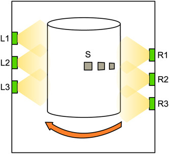
Thin films were deposited from ternary Ti3SiC2 cathodes (Maxthal) of a so-called MAX phase,Reference Barsoum18 prepared in bulk form and commercially available. A schematic of the industrial scale cathodic arc evaporation system (Sulzer Metaplas MZR 323) is shown in Fig. 1. Polished cemented carbide substrates, S, of WC with 10 wt.% Co were placed on a cylinder rotating at 3 rpm about 15 cm in front of the cathodes, operated at an arc current of 50 A dc. The substrates were negatively biased at −30 V. The chamber was heated through resistive heating elements located on the far chamber side to a temperature of ∼400 °C on the rotating cylinder. Nitrogen was introduced at pressures between 0 and 6 Pa, to form a reactive atmosphere. During nonreactive deposition, a small addition of Ar, ∼0.1 Pa, was needed to sustain the arc. The deposition pressure of N2 is hereafter abbreviated pN2. The base pressure was ∼10−3 Pa and all films were deposited to a thickness in the range 3–5 μm.
Schematic drawing of the deposition system. Cathodes are denoted L1–L3 and R1–R3, and substrates are denoted S.

Film and cathode compositions were analyzed by elastic recoil detection analysis with a time-of-flight and energy detector (TOF-E ERDA), using a 40 MeV 127I9+ ion beam at 22.5° incidence angle relative to the surface. The resulting time-of-flight versus recoil energy spectra were evaluated using the CONTES code.Reference Jansson19
X-ray diffractometry (XRD) for phase analysis was performed using a Bruker AXS D8-advanced x-ray diffractometer with a line-focus Cu Kα x-ray source. θ-2θ scans were recorded in the 2θ-range from 2 to 80°. Structural characterization was performed through transmission electron microscopy (TEM) using an analytical FEI Tecnai G2 TF 20 UT microscope equipped with an energy dispersive x-ray spectrometer. Cross-sectional TEM (XTEM) samples were prepared through mechanical polishing and ion milling. Surface morphology was characterized using a LEO 1550 scanning electron microscope (SEM) operated at 5 kV.
Chemical bonding state analysis through x-ray photoelectron spectroscopy (XPS) was performed in a Scienta ESCA200 spectrometer, using a monochromatized Al(Kα) x-ray source with photon energy hν = 1486.6 eV. The samples were not sputter cleaned prior to measurement to avoid preferential sputtering and sputter-induced chemistry. The graphite C1s position at 284.6 eV was used as reference for the energy calibration and a Shirley-type background subtraction was used in data analysis.
Film hardness was measured on polished tapered cross sections, using a UMIS nanoindenter equipped with a Berkovich diamond tip. Approximately 20 indents were made for each sample to an indentation depth of ∼0.2 μm, corresponding to a maximum applied load of 15–40 mN. Hardness was evaluated using the method proposed by Oliver and Pharr.Reference Oliver and Pharr20
III. RESULTS AND DISCUSSION
A. Composition
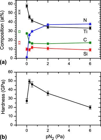
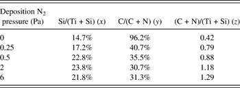
Figure 2(a) shows the composition of the Ti–Si–C–N films as a function of N2 deposition pressure. All films are rich in Si and C, with compositions in the range 10–12 and 16–28 at.%, respectively. Arcing from Ti3SiC2 cathodes without reactive gas yielded films with 10 at.% Si and 28 at.% C, which is lower compared to the cathode composition; the latter was confirmed by ERDA within a few at.% of the nominal composition of 17 at.% Si and 33 at.% C. The compositional difference between cathode and film can, at least in part, be attributed to preferential re-sputtering.Reference Eriksson, Zhu, Ghafoor, Johansson, Sjölén, Jensen, Odén, Hultman and Rosén21 The N content increases with increase in N2 pressure up to 37 at.% at pN2 = 2 Pa. Further increase in pressure gives only small compositional changes, and the system is therefore considered to have reached a point of saturation. Films grown in the presence of N2 have lower concentrations of Ti and C if compared to the pN2 = 0 Pa deposition. The decrease is slightly larger than predicted from the plain effect of dilution. For the samples deposited at pN2 = 2–6 Pa, ∼38 at.% Ti would be expected if the ratios between Ti, Si, and C were preserved from the pN2 = 0 Pa deposition, which contrasts the measured 34 at.%. The Si content remains relatively stable at 10–12 at.% throughout the whole series. Using an alternative notation, see Table I, the film with maximum Si content, deposited at pN2 = 0.5 Pa, can also be described as (Ti0.77Si0.23)(C0.35N0.65)0.88. The compositional ratio between C and N on the one side and Ti and Si on the other side varies considerably from 0.42 in the sample deposited without N2 up to 1.29 when the highest N2 pressure was used. The apparent overstoichiometry, with respect to TiN and TiC, at high pN2 can be explained by the presence of Si3N4, CNx, and related phases that coordinate more N than the cubic (Ti,Si)(C,N) phase, as discussed later. The indicated N content at pN2 = 0 Pa in Table I corresponds to ∼1 at.%, as presented in Fig. 2. This is below the level of O contamination of 1–4 at.% present in all samples. However, both C and O can be slightly overestimated in ERDA analysis because of rough sample surfaces. The Si and C contents exceed the values reported from arcing TiSi cathodes (compromising up to 20 at.% Si) in CH4 and N2, where the maximum incorporation of Si and C was in (Ti0.86Si0.14)(C0.28N0.72)0.87.Reference Johnson, Rogström, Johansson, Odén and Hultman16 The use of ternary cathodes is thus one way to extend the range of attainable compositions in Ti–Si–C–N films grown by arc deposition. Beyond this method, PECVD synthesis of C-rich films with Si contents up to 11.6 at.% have been reported. This corresponds to (Ti0.77Si0.23)(C0.77N0.23)0.95, with a microstructure composed of Ti(C,N), SiC, and Ti2C phases.Reference Guo, Ma, Xu, Bell, Li and Dong22 As shown later, the films investigated in this study consist primarily of cubic (Ti,Si)(C,N) phase. The Si and C contents are henceforth presented in at% of total composition, as given in Fig. 2(a).
(a) Film composition in at.% as a function of N2 deposition pressure (the cathode composition is indicated by open symbols) and (b) film hardness.

Film composition expressed as stoichiometry factors in (Ti1−xSix)(CyN1−y)z.

The compositional variations determined by ERDA are strongly correlated to film hardness, as shown in Fig. 2(b). The hardness maximum is found for films deposited at pN2 = 0.25 and 0.5 Pa, which corresponds to intermediate N-content. However, a detailed interpretation of these results also requires investigation of microstructure and chemical bonding, as presented later.
B. Microstructure and nanostructure
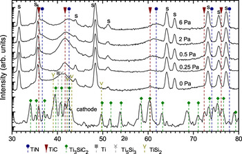
Results from XRD analysis are presented in Fig. 3. In addition to peaks from the WC-Co substrate, the sample deposited without reactive gas shows a broad feature in the region from 30 to 50° (2θ). Its maximum, in a broad plateau at 41–42°, encompasses the reference position of the TiC 200 peak, as well as peaks from Ti, Ti5Si3, and TiSi2.23 The presence of these metallic and silicide phases is supported by XPS data presented later. An additional small peak located at 2θ = 61° overlaps with TiC. No signs of Ti3SiC2 were found for measurements down to 2θ = 5°, which is unsurprising since the film composition deviates from the MAX-phase stoichiometry also for nonreactive growth. The broad XRD-peaks can be explained by stress or small crystallite size on the nanometer scale, the latter as evidenced by high resolution TEM (HRTEM).
X-ray diffractometry pattern from Ti–Si–C–N films and the Ti3SiC2 cathode. S denotes substrate peak.

For films deposited in a N2 environment, more distinct peaks appear corresponding to an fcc-structure with lattice parameters between references for TiC and TiN.23 The 200 peak at ∼42° has a maximum intensity for films deposited at pN2 = 0.5 Pa. The 111 peak at 36–37° partly overlaps with a substrate peak and the most visible shoulder is in the two samples deposited at pN2 = 2 and 6 Pa. The 220 peak, identified at 61–62°, also has substantial broadening. A small shift of this peak toward higher angles can be observed with increasing N content. This is likely to be the effect of a decreasing lattice parameter as N replaces C in the cubic structure, though concomitant change in the intrinsic stress level cannot be ruled out. Although distinct XRD peaks without substrate overlap is required for exact stress measurements, the present sin2ψ measurements of the 200 peaks indicate a substantial compressive stress of 5–7 GPa, assuming an E-modulus of 450 GPa.Reference Sue24 We also note that Si substituting for Ti in TiN does not give detectable shifts in the lattice parameter.Reference Flink, Beckers, Sjölen, Larsson, Braun, Karlsson and Hultman1
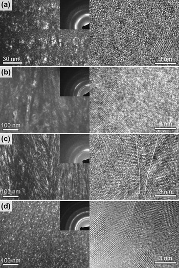
Figure 4 shows dark field (to the left) and high resolution (to the right) XTEM micrographs from films deposited at different N2 pressures. At pN2 = 0 Pa [Fig. 4(a)], the structure is fully crystalline and comprises 2–7 nm large equiaxed grains. The film exhibits a 002 preferred crystallographic orientation, as indicated by the selected area electron diffraction (SAED) pattern, in agreement with the XRD results. For the film deposited at pN2 = 0.25 Pa, shown in Fig. 4(b), the microstructure is columnar with ∼10–15 nm wide grains, resulting again in the 002 texture.
Dark-field transmission electron micrographs (TEM) with corresponding selected area electron diffraction pattern insets (to the left) and high resolution TEM images (to the right) of samples grown with pN2 equal to (a) 0 Pa, (b) 0.25 Pa, (c) 0.5 Pa, and (d) 6 Pa. The trace of {200} lattice planes of two grains is indicated in (c).

At pN2 = 0.5 Pa, shown in Fig. 4(c), a feather-like microstructure appears. It consists of bundles of nano-size crystallites fanning out from the substrate normal, as can be seen in both the dark-field and HRTEM modes. The trace of {200} lattice planes of two diverging grains are indicated in the figure. This nanostructure with semicoherent crystallites has previously been observed in arc-deposited Ti–Si–NReference Flink, Beckers, Sjölen, Larsson, Braun, Karlsson and Hultman1, Reference Flink, Larsson, Sjölen, Karlsson and Hultman25 and Ti–Si–C–NReference Johnson, Rogström, Johansson, Odén and Hultman16 films. The suggested explanation involves Si segregation on the coating surface, which leads to repeated renucleation of (002)-textured Ti(C)N subgrains and eventual Si3N4 precipitation. Si-vacancy-stabilized cubic-like SiNx (x ≈ 1.33) may also form in contact with TiN.Reference Flink, Beckers, Sjölen, Larsson, Braun, Karlsson and Hultman1, Reference Marten, Isaev, Alling, Hultman and Abrikosov26, Reference Hultman, Bareño, Flink, Söderberg, Larsson, Petrova, Odén, Greene and Petrov27 The pronounced 002 texture in the films deposited at pN2 = 0.5 Pa is similar to what was reported by Flink et al.Reference Flink, Beckers, Sjölen, Larsson, Braun, Karlsson and Hultman1
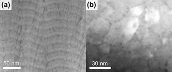
At the highest N content (pN2 = 6 Pa), the sample consists of fine grains of a few nanometers [Fig. 4(d)]. Low-density areas at apparent column boundaries were visible in underfocused bright-field imaging (not shown here). The HRTEM imaging indicates a fine-grained defect-rich structure without voids, but with possible amorphous domains. Any amorphous phase, however, would have very minor volume fraction of the material, as the SAED diffraction pattern features only fcc reflections, but no amorphous rings. A coarser (50-nm scale) STEM imaging in Fig. 5(a) shows that there exists a superimposed, apparently columnar, structure along the growth direction, with 3–5 nm wide rod-like features. The rod contrast suggests that these areas consist of elements lighter than Ti. The banded horizontal layering visible in the image, and present in all samples investigated, is an effect of sample rotation in the high-capacity commercial coating systems, as described in detail elsewhere.Reference Eriksson, Zhu, Ghafoor, Johansson, Sjölén, Jensen, Odén, Hultman and Rosén21 We note that the rod-like features track valleys in the film surface in each stage of deposition, indicated by the layers. In plan view STEM [Fig. 5(b)], we see that the light element areas decorate the grain boundaries. Hence, the extremely fine-grained structure and the rod-like features in the pN2 = 6 Pa film is a strong indication that Si and possibly C segregate at the film surface during growth and reacts to some extent with N supplied from the gas ambient.
(a) Scanning TEM of a pN2 = 6 Pa sample, indicating segregation of light elements as dark rods in cross section. (b) In plan view, the light elements appear at grain boundaries.

C. Chemical bonding state
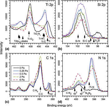
XPS peak profiles for Ti2p, Si2p, C1s, and N1s core levels are presented in Figs. 6(a)–6(d). The Ti2p spectra in Fig. 6(a) are the most complex one since there are two asymmetrical core level lines (Ti2p3/2 and Ti2p1/2) associated with each chemical state of the Ti atom. However, the spin split between Ti2p3/2 and Ti2p1/2 signals is ∼6 eV, i.e., larger than the accounted chemical shifts, which facilitates analysis. We base the discussion on the Ti2p3/2 core levels that comprise the binding energy region between 452 and 459 eV. The corresponding Ti2p1/2 signals appear at the binding energies higher than 459 eV and are not referred to in the text below. In the case of Si2p, the energy split between Si2p3/2 and Si2p1/2 core level components is smaller than the experimental resolution; hence, there is a one-to-one correspondence between spectral features and chemical states of the Si atom.
X-ray photoelectron spectroscopy peak profiles from samples grown at different N2 pressures.

The sample deposited without N2 shows peaks corresponding to Ti–C bonds at 454 eV in the Ti2p3/2 spectra and at ∼281 eV in the C1s spectra. There is likely a fraction of Ti–Ti or Ti–Si bonds contributing to the peak at 454 eV in Fig. 6(a). A peak at ∼98 eV corresponding to Si–Si or Si–Ti can also be observed in the Si2p spectra. The presence of Ti, and of potentially intermetallic TiSix phases, is consistent with XRD results for the pN2 = 0 Pa sample, where also no diffraction peaks from Si are present. The slight shift of some of the XPS peaks toward lower binding energy relative to references is likely the effect of different charging states compared to the phase or region with C–C bonds used for binding energy calibration. In the two samples with intermediate N content, deposited at pN2 = 0.25 and 0.5 Pa, the Ti–C peaks in Ti2p and C1s spectra are shifted about 0.5 eV toward higher binding energy. This can be explained by a decreased net negative charge density on Ti and C atoms in the Ti–C lattice, caused by nitridation. As N has a higher electronegativity than C, the corresponding Ti2p and C1s core levels experience a shift towards higher binding energy as N substitutes C in the Ti–C–N lattice. The trend toward an XPS spectrum of a more TiN-like character at higher N2 deposition pressure is supported by the shift of the Ti(C,N) 220 XRD diffraction peak toward the TiN reference position at high N content (Fig. 3). In the N1s spectra, Ti–N bonds appear with a slight broadening toward lower binding energy at increased N content, which is likely an effect of C. Bonding in the quarternary system can thus be described as a carbonitride, in the sense that the presence of N affects C and vice versa. Since the crystalline structure is TiN-like NaCl-structure, we suggest simultaneous solid solubility of Si on the Ti sublattice and C on the N sublattice into combined (Ti,Si)(C,N), which constitutes the nanosized grains in the structure.
At still higher N content, in the samples deposited at pN2 = 2 and 6 Pa, the Ti–C components vanish from the XPS profile, indicating that Ti has a clear bonding preference for N rather than C. These N levels correspond to compositional saturation as determined by ERDA. Still, the N1s core level signal assigned to Ti–N at ∼397 eV is most intense for the 0.25 and 0.5 Pa samples, and with increasing N content the peak is broadened toward lower binding energies. Simultaneously, a broad peak at ∼399 eV emerges in the N1s spectra. This feature is attributed to C–Nx type bonds, which are reported around 400 eV binding energy depending on the type of hybridization.Reference Snis and Matar28 Such C–N bonds would also be responsible for the shoulder at 286 eV in the C1s spectra, and of higher intensity with increasing N content. Signs of C–N bonds on the C1s peak have previously been reported in Ti–Si–C–NReference Jedrzejowski, Klemberg-Sapieha and Martinu8 and Ti–C–NReference Lu, Shen, Zhou and Li29 films, where C–C and C–N bonds are allegedly present in an amorphous matrix surrounding 5–15 nm large Ti(C,N) grains.Reference Lu, Shen, Zhou and Li29 These reports do not, however, identify corresponding peaks in the N1s spectra, despite that this is a determining peak for CNx.Reference Snis and Matar28, Reference Hellgren, Johansson, Broitman, Hultman and Sundgren30 This suggests that our clear features at ∼400 eV correspond to a comparatively higher amount of C–N bonds. Nevertheless, the relative volume and ordering of CNx compounds must be limited as no electron diffractionReference Neidhardt, Hultman and Czigány31 intensity was revealed from the samples (Fig. 4).
The peak from C–C bonds at 284.6 eV is dominant in the C1s spectra and to a large extent caused by surface contamination. Hence, no information is given about presence or prevalence of C–C bonds in film. There are also Ti2p3/2 peaks present from TiO2 at 459 eV and an oxynitride, TiOxNy, at ∼456.5 eV, causing the plateau-like shape in the Ti2p3/2 spectra for the pN2 = 2 and 6 Pa samples.
The Si2p profile for the pN2 = 0 Pa sample has, in addition to the broad peak at ∼98 eV, a second peak at ∼102 eV corresponding to Si–N bonds, as in Si3N4. With increasing N2 deposition pressure, the Si–N peak is broadened and shifted toward lower binding energies, indicating the formation of Si–C bonds. Furthermore, in the N1s spectra, Si–N bonds might also be present as a minor component at 398 eV, between the Ti–N and C–Nx peaks. The formation of Si3N4, previously reported in the quarternary system studied here,Reference Abraham, Choi, Kang and Kim3, Reference Guo, Ma and Xu7, Reference Ma, Ma, Dong, Xu and Bell9 is thus possible but not dominating. In our experiments, no signature of Si3N4 was detected from XRD, indicating that the phase, if present, is amorphous.
D. Surface morphology
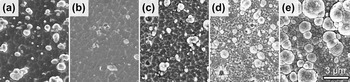
The surface morphology of the films, as imaged by SEM in Fig. 7, changes from rather smooth for intermediate N content, to very rough at the high end of the N2 deposition pressure. At pN2 = 6 Pa, the surface has a rugged structure, which can be correlated with the undulating growth layers in Fig. 5, where the segregation of light elements is destined for the valleys. The rough surface morphology is connected with the limited surface diffusion as a result of low growth temperature and low energy fluxReference Anders32 applied here, and the effect of macroparticle incorporation resulting from arc deposition.Reference Anders33 Hence, the change in morphology can also be explained by the generally observed decrease in ion flux and ion energy with increasing deposition pressure (see, for example, Ref. Reference Rosén, Anders, Mraz, Atiser and Schneider34), limiting the total energy supplied to the surface. The segregation and the dense crystalline structure determined by TEM do, however, suggest some surface diffusion.
Scanning electron microscope images from Ti–Si–C–N films grown at pN2 equal to (a) 0 Pa, (b) 0.25 Pa, (c) 0.5 Pa, (d) 2 Pa, and (e) 6 Pa.

E. Mechanical properties
The hardness of the films is presented in Fig. 2(b). The film deposited at pN2 = 0 Pa, with partly carbide character, shows a modest hardness of 27 GPa, somewhat higher than Ti–Si–C nanocomposite films (20 GPa),Reference Eklund35 but lower compared to TiC films (36 GPa).Reference Karlsson, Hultman, Johansson, Sundgren and Ljungcrantz2 Hence, the film structure may be weakened by the presence of Ti and TiSix phases. The enhanced hardness, up to 49 GPa, at intermediate N content, can be explained by the feathered microstructure of highly ordered small grains with strong interconnection that restrict movement of grains and dislocations in response to deformation. These properties may be further enhanced by Si- and C-rich tissue phases, as seen in Ti–Si–N.Reference Flink, Beckers, Sjölen, Larsson, Braun, Karlsson and Hultman1 For the pN2 = 6 Pa sample, the decreased hardness is combined with loss of the strong directional bonding present in the feathered structure at lower N content. The grain orientation is random, typically with high-angle grain boundaries [Fig. 4(c)]. We suggest that the cohesion of the material is weakened by the segregating grain boundary phases.
The hardness maximum covers the region where the feathered structure was detected in TEM and where the XPS results indicate a Ti–Si–C–N solid solution. Arc-deposited Ti–Si–N films have been reported with a maximum hardness of 42 GPa, corresponding to a Si-content of 6.5 at%, where the hardening was attributed to defects, solid solution, grain size, and coherency strain with crystalline SiNx at grain boundaries.Reference Flink, Beckers, Sjölen, Larsson, Braun, Karlsson and Hultman1 Similar hardness, 38–40 GPa, was also found in arc-deposited Ti–Si–C–N films from binary Ti–Si cathodes.Reference Johnson, Rogström, Johansson, Odén and Hultman16 In both cases, the films exhibit the feather-like microstructure. For PECVD-grown Ti–Si–C–N-films, hardness up to 48 GPa has been reported under C-rich conditions for which a structure forms with nanocrystalline Ti(C,N) and amorphous C and Si3N4.Reference Guo, Ma and Xu7
Previous reports on Ti–C–N films discuss different hardening mechanisms. Lu et al.Reference Lu, Shen, Zhou and Li29 investigated Ti–C–N coatings with various C content grown by reactive unbalanced magnetron sputtering. The maximum hardness of 49 GPa was obtained for 12.5 at.% C, attributed to solid-solution hardening and high residual stress. At higher C content, a nanocomposite structure was formed, consisting of Ti(C,N) grains in an amorphous matrix containing C and CNx, with drastically lower hardness and compressive stress.Reference Lu, Shen, Zhou and Li29 Arc-deposited Ti–C–N films with a maximum hardness of 45 GPa, corresponding to a C content of ∼28 at.%, were studied by Karlsson et al.Reference Karlsson, Hultman, Johansson, Sundgren and Ljungcrantz2 The hardness was explained by an increasing bond strength as the covalent character increases when C replaces N, combined with strain induced by defect density, which was found largest in the range of maximum hardness. In our case, all samples exhibit significant defect density, relatively high residual stress, and small grain size, all of which likely contributes to the detected film hardness. The difference between our samples is, however, primarily related to the microstructural differences induced by a changed composition.
F. Segregation of Si and C in the Ti–Si–C–N films
Films deposited with the Ti3SiC2 compound cathodes are rich in Si and C, each of which are known to enhance mechanical properties of TiN by promoting grain refinement and defect generation. Our results show that with simultaneous high content of Si and C, the amount of N requires delicate control to avoid segregation and precipitation of weak grain boundary phases based on Si, C, and N. As evident from XRD and TEM analysis, the film growth promotes the B1 NaCl-structure, which cannot accommodate all compositions tested in this study. In growth without N2, the film can be considered to consist of understoichiometric TiCx, with possible Si substitutions together with Ti and silicide phases.
In the partially nitrided films, deposited at pN2 = 0.25 and 0.5 Pa, the cubic-phase (Ti,Si)(C,N) grains arrange in the feathered structure known from Ti–Si–N. Grains are needle-like here, as a result of surface-diffusion mediated segregation that limits lateral grain growth, and with grown-in defects that form semicoherent sub-grains. As discussed in Ref. Reference Flink, Beckers, Sjölen, Larsson, Braun, Karlsson and Hultman1, epitaxial monolayer-thick tissue phases of SiNx may be formed.
At higher N content, pN2 = 6 Pa, the segregation of Si and C is so extensive that it leads to the formation of nanometer-thick grain boundary phases of CNx and possibly Si3N4 as determined by STEM and XPS analysis. At the same time, the renucleation rate of the cubic phase on the film surface increases, resulting in an equiaxed grain structure with no preferential orientation in these samples. Since CNx (and Si3N4) are incoherent phases with lower hardness than the cubic Ti(C,N), this extensive segregation reduces the total film hardness. Thus, in abundance of N, the combined presence of Si and C disturbs cubic phase growth severely and compromises mechanical strength of the films.
IV. CONCLUSIONS
Predominantly cubic Ti–Si–C–N alloy thin films with a wide range of compositions can be deposited by arc evaporation from Ti3SiC2 compound cathodes at varying N2 pressures. Without reactive gas, the films consist of a mixture of TiCx and metallic phases (Ti, TiSix) and have a moderate hardness of 27 GPa. Superhard, up to 49 GPa, (Ti,Si)(C,N) films with a nanocrystalline feathered structure of primarily cubic phase form at pN2 = 0.25–0.5 Pa. Above pN2 = 2 Pa, which corresponds to saturation of N content, the crystalline phases obtain a pronounced nitride character. At the same time, C and Si segregate to microscopic column and nanoscopic grain boundaries, which weaken the material’s strength.
While Si and C added separately have beneficial effects on the hardening of TiN through effective grain refinement and solid solution hardening, their combined presence in high concentrations, together with N, accelerates the phase separation into incoherent CNx and possibly Si3N4 and thus degrades the mechanical properties of Ti–Si–C–N films.
ACKNOWLEDGMENTS
This work was funded by the VINN Excellence center on Functional Nanoscale Materials (FunMat). The authors also acknowledge Uppsala University for access to the Tandem Laboratory for ERDA analysis.